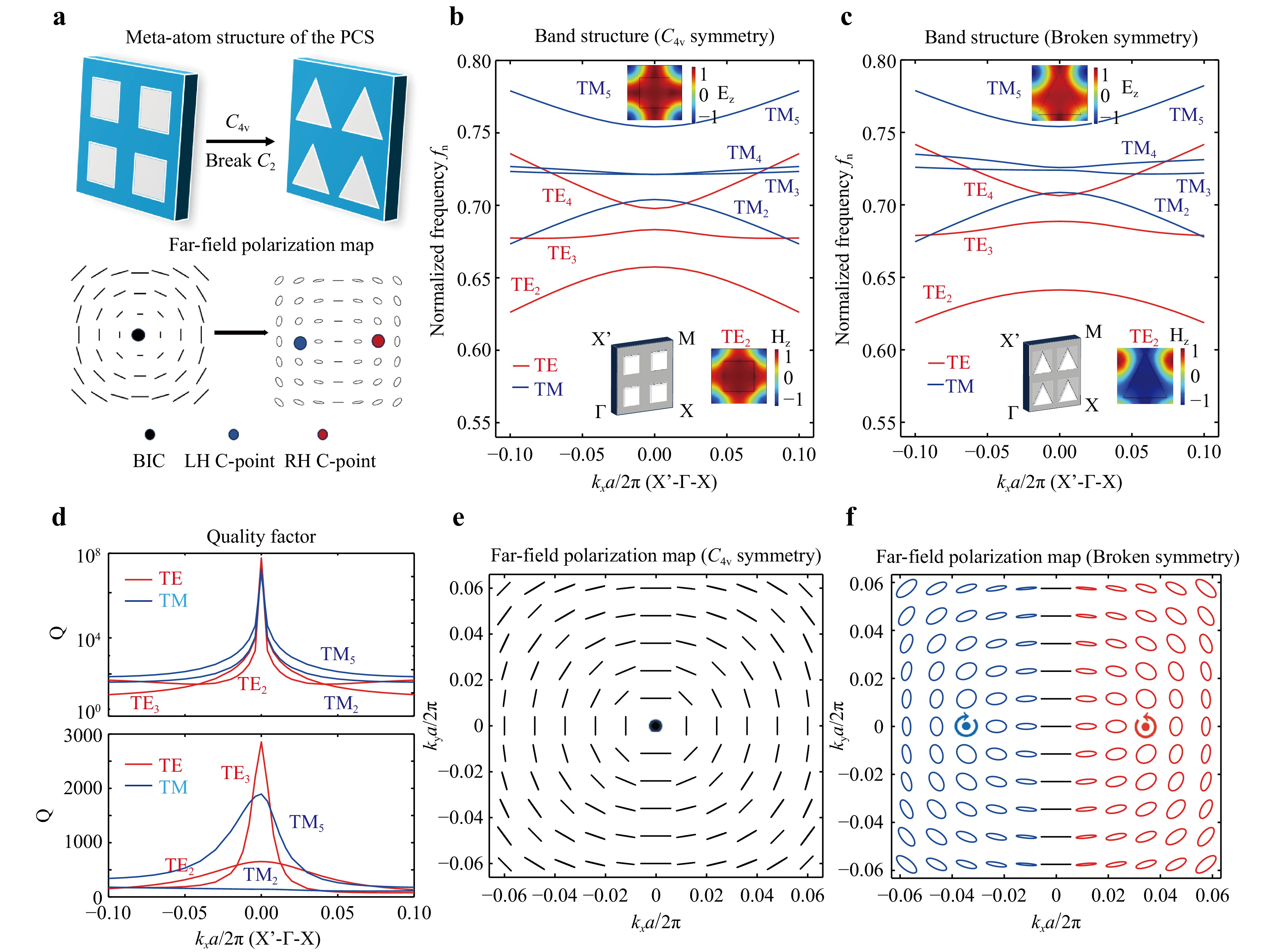
Holographic displays have the promise to be the ultimate 3D display technology, able to account for all visual cues. Recent advances in photonics and electronics gave rise to high-resolution holographic display prototypes, indicating that they may become widely available in the near future. One major challenge in driving those display systems is computational: computer generated holography (CGH) consists of numerically simulating diffraction, which is very computationally intensive. Our goal in this paper is to give a broad overview of the state-of-the-art in CGH. We make a classification of modern CGH algorithms, we describe different algorithmic CGH acceleration techniques, discuss the latest dedicated hardware solutions and indicate how to evaluate the perceptual quality of CGH. We summarize our findings, discuss remaining challenges and make projections on the future of CGH.
Fabry–Perot (F–P)-based phase demodulation of heterodyne light-induced thermoelastic spectroscopy (H-LITES) was demonstrated for the first time in this study. The vibration of a quartz tuning fork (QTF) was detected using the F–P interference principle instead of an electrical signal through the piezoelectric effect of the QTF in traditional LITES to avoid thermal noise. Given that an Fabry–Perot interferometer (FPI) is vulnerable to disturbances, a phase demodulation method that has been demonstrated theoretically and experimentally to be an effective solution for instability was used in H-LITES. The sensitivity of the F–P phase demodulation method based on the H-LITES sensor was not associated with the wavelength or power of the probe laser. Thus, stabilising the quadrature working point (Q-point) was no longer necessary. This new method of phase demodulation is structurally simple and was found to be resistant to interference from light sources and the surroundings using the LITES technique.
Optimizing laser processes is historically challenging, requiring extensive and costly experimentation. To solve this issue, we apply Bayesian optimization for process parameter optimization to laser cutting, welding, and polishing. We demonstrate how readily available Bayesian optimization frameworks enable efficient optimization of laser processes with only modest expert knowledge. Case studies on laser cutting, welding, and polishing highlight its adaptability to real-world manufacturing scenarios. Moreover, the examples emphasize that with suitable cost functions and boundaries an acceptable optimization result can be achieved after a reasonable number of experiments.
Silicon photonics is currently the leading technology for the development of compact and low-cost photonic integrated circuits. However, despite its enormous potential, certain limitations, such as the absence of a linear electro-optical (EO) effect because of the symmetric crystal structure of silicon remain. In contrast, barium titanate (BTO) exhibits a strong Pockels effect. In this study, we demonstrated a high-quality transferred barium titanate ferroelectric hybrid integrated modulator on a silicon-on-insulator platform. The proposed hybrid integration of BTO on silicon Mach-Zehnder interferometers exhibited EO modulation with a VπL as low as 1.67 V·cm, thereby facilitating the realisation of compact EO modulators. The hybrid integration of BTO with SOI waveguides is expected to pave the way for the development of high-speed and high efficiency EO modulators.
Over the last few decades, ultrafast laser processing has become a widely used tool for manufacturing microstructures and nanostructures. The real-time monitoring of laser material processing provides opportunities to inspect processes and provide feedback. To date, in-situ and real-time monitoring of laser material processing has rarely been performed. To this end, we propose dual-path snapshot compressive microscopy (DP-SCM) for high-speed, large field-of-view, and high-resolution imaging for in-situ and real-time ultrafast laser processing. In the evaluation of DP-SCM, the field of view, lateral resolution, and imaging speed were measured to be 2 mm, 775 nm, and 500 fps, respectively. In ultrafast laser processing, the laser scanning process is observed using a DP-SCM system when translating the sample stage and scanning the focused femtosecond laser. Finally, we monitored the development of a self-organized nanograting structure to validate the potential of our system for unveiling new material mechanisms. The proposed method serves as an add-up (plug-and-play) module for any imaging setup and has vast potential for opening new avenues for high-throughput imaging in laser material processing.
The demand for optical glass has been rapidly increasing in various industries, where an ultra-smooth surface and form accuracy are critical for the functional elements of the applications. To meet the high surface-quality requirements, a polishing process is usually adopted to finish the optical glass surface to ensure an ultra-smooth surface and eliminate sub-surface damage. However, current ultra-precision polishing processes normally polish workpieces individually, leading to a low production efficiency and high polishing costs. Current mass-finishing methods cannot be used for optical glasses. Therefore, magnetic-field-assisted batch polishing (MABP) was proposed in this study to overcome this research gap and provide an efficient and cost-effective method for industrial use. A series of polishing experiments were conducted on typical optical components under different polishing parameters to evaluate the polishing performance of MABP on optical glasses. The results demonstrated that MABP is an efficient method to simultaneously polish multiple lenses while achieving a surface roughness, indicated by the arithmetic mean height (Sa), of 0.7 nm and maintained a sub-micrometer surface form for all the workpieces. In addition, no apparent sub-surface damage was observed, indicating the significant potential for the high-quality rapid polishing of optical glasses. The proposed method is highly competitive compared to the current optical polishing methods, which has the potential to revolutionize the polishing process for small optics.
Emission of THz radiation from air breakdown at focused ultra-short fs-laser pulses (800 nm/35 fs) was investigated for the 3D spatio-temporal control where two pre-pulses are used before the main-pulse. The laser pulse induced air breakdown forms a ~ 120 μm-long focal volume generate shockwaves which deliver a denser air into the focal region of the main pulse for enhanced generation of THz radiation at 0.1–2.5 THz spectral window. The intensity of pre- and main-pulses was at the tunnelling ionisation intensities (1–3) × 1016 W/cm2 and corresponded to sub-critical (transparent) plasma formation in air. Polarisation analysis of THz radiation revealed that orientation of the air density gradients generated by pre-pulses and their time-position locations defined the ellipticity of the generated THz electrical field. The rotational component of electric current is the origin of THz radiation.
State-of-the-art commercially available 3D laser micro- and nanoprinters using polymeric photoresists based on two- or multi-photon absorption rely on high-power pico- or femtosecond lasers, leading to fairly large and expensive instruments. Lately, we have introduced photoresists based on two-step absorption instead of two-photon absorption, allowing for the use of small and inexpensive continuous-wave 405 nm wavelength GaN semiconductor laser diodes with light-output powers below 1 mW. Here, using the identical photoresist system and similar laser diodes, we report on the design, construction, and characterization of a 3D laser nanoprinter that fits into a shoe box. This shoe box contains all optical components, namely the mounted laser, the collimation- and beam-shaping optics, a miniature MEMS xy-scanner, a tube lens, the focusing microscope objective lens (NA=1.4, 100× magnification), a piezo slip-stick z-stage, the sample holder, a camera monitoring system, LED sample illumination, as well as the miniaturized control electronics employing a microcontroller. We present a gallery of example 3D structures printed with this instrument. We achieve about 100 nm lateral spatial resolution and focus scan speeds of about 1 mm/s. Potentially, our shoe-box-sized system can be made orders of magnitude less expensive than today’ s commercial systems.
Organic proteins are attractive owing to their unique optical properties, remarkable mechanical characteristics, and biocompatibility. Manufacturing multifunctional structures on organic protein films is essential for practical applications; however, the controllable fabrication of specific structures remains challenging. Herein, we propose a strategy for creating specific structures on silk film surfaces by modulating the bulging and ablation of organic materials. Unique surface morphologies such as bulges and craters with continuously varying diameters were generated based on the controlled ultrafast laser-induced crystal-form transition and plasma ablation of the silk protein. Owing to the anisotropic optical properties of the bulge/crater structures with different periods, the fabricated organic films can be used for large-scale inkless color printing. By simultaneously engineering bulge/crater structures, we designed and demonstrated organic film-based optical functional devices that achieves holographic imaging and optical focusing. This study provides a promising strategy for the fabrication of multifunctional micro/nanostructures that can broaden the potential applications of organic materials.
We describe how a direct combination of an axicon and a lens can represent a simple and efficient beam-shaping solution for laser material processing applications. We produce high-angle pseudo-Bessel micro-beams at 1550 nm, which would be difficult to produce by other methods. Combined with appropriate stretching of femtosecond pulses, we access optimized conditions inside semiconductors allowing us to develop high-aspect-ratio refractive-index writing methods. Using ultrafast microscopy techniques, we characterize the delivered local intensities and the triggered ionization dynamics inside silicon with 200-fs and 50-ps pulses. While similar plasma densities are produced in both cases, we show that repeated picosecond irradiation induces permanent modifications spontaneously growing shot-after-shot in the direction of the laser beam from front-surface damage to the back side of irradiated silicon wafers. The conditions for direct microexplosion and microchannel drilling similar to those today demonstrated for dielectrics still remain inaccessible. Nonetheless, this work evidences higher energy densities than those previously achieved in semiconductors and a novel percussion writing modality to create structures in silicon with aspect ratios exceeding ~700 without any motion of the beam. The estimated transient change of conductivity and measured ionization fronts at near luminal speed along the observed microplasma channels support the vision of vertical electrical connections optically controllable at GHz repetition rates. The permanent silicon modifications obtained by percussion writing are light-guiding structures according to a measured positive refractive index change exceeding 10−2. These findings open the door to unique monolithic solutions for electrical and optical through-silicon-vias which are key elements for vertical interconnections in 3D chip stacks.
Mode-division multiplexing technology has been proposed as a crucial technique for enhancing communication capacity and alleviating growing communication demands. Optical switching, which is an essential component of optical communication systems, enables information exchange between channels. However, existing optical switching solutions are inadequate for addressing flexible information exchange among the mode channels. In this study, we introduced a flexible mode switching system in a multimode fibre based on an optical neural network chip. This system utilised the flexibility of on-chip optical neural networks along with an all-fibre orbital angular momentum (OAM) mode multiplexer-demultiplexer to achieve mode switching among the three OAM modes within a multimode fibre. The system adopted an improved gradient descent algorithm to achieve training for arbitrary 3 × 3 exchange matrices and ensured maximum crosstalk of less than −18.7 dB, thus enabling arbitrary inter-mode channel information exchange. The proposed optical-neural-network-based mode-switching system was experimentally validated by successfully transmitting different modulation formats across various modes. This innovative solution holds promise for providing effective optical switching in practical multimode communication networks.
Dwell time plays a vital role in determining the accuracy and convergence of the computer-controlled optical surfacing process. However, optimizing dwell time presents a challenge due to its ill-posed nature, resulting in non-unique solutions. To address this issue, several well-known methods have emerged, including the iterative, Bayesian, Fourier transform, and matrix-form methods. Despite their independent development, these methods share common objectives, such as minimizing residual errors, ensuring dwell time's positivity and smoothness, minimizing total processing time, and enabling flexible dwell positions. This paper aims to comprehensively review the existing dwell time optimization methods, explore their interrelationships, provide insights for their effective implementations, evaluate their performances, and ultimately propose a unified dwell time optimization methodology.
Optical micro/nanofibers (MNFs) taper-drawn from silica fibers possess intriguing optical and mechanical properties. Recently, MNF array or MNFs with identical geometries have been attracting more and more attention, however, current fabrication technique can draw only one MNF at a time, with a low drawing speed (typically 0.1 mm/s) and a complicated process for high-precision control, making it inefficient in fabricating multiple MNFs. Here, we propose a parallel-fabrication approach to simultaneously drawing multiple (up to 20) MNFs with almost identical geometries. For fiber diameter larger than 500 nm, measured optical transmittances of all as-drawn MNFs exceed 96.7% at 1550-nm wavelength, with a diameter deviation within 5%. Our results pave a way towards high-yield fabrication of MNFs that may find applications from MNF-based optical sensors, optical manipulation to fiber-to-chip interconnection.
Microwave antennas are essential elements for various applications, such as telecommunication, radar, sensing, and wireless power transport. These antennas are conventionally manufactured on rigid substrates using opaque materials, such as metal strips, metallic tapes, or epoxy pastes; thus, prohibiting their use in flexible and wearable devices, and simultaneously limiting their integration into existing optoelectronic systems. Here, we demonstrate that mechanically flexible and optically transparent microwave antennas with high operational efficiencies can be readily fabricated using composite nanolayers deposited on common plastic substrates. The composite nanolayer structure consists of an ultra-thin copper-doped silver film sandwiched between two dielectric films of tantalum pentoxide and aluminum oxide. The material and thickness of each constituent layer are judiciously selected such that the whole structure exhibits an experimentally measured averaged visible transmittance as high as 98.94% compared to a bare plastic substrate, and simultaneously, a sheet resistance as low as 12.5 Ω/sq. Four representative types of microwave antennas are implemented: an omnidirectional dipole antenna, unidirectional Yagi-Uda antenna, low-profile patch antenna, and Fabry-Pérot cavity antenna. These devices exhibit great mechanical flexibility with bending angle over 70°, high gain of up to 13.6 dBi, and large radiation efficiency of up to 84.5%. The proposed nano-engineered composites can be easily prepared over large areas on various types of substrates and simultaneously overcome the limitations of poor mechanical flexibility, low electrical conductivity, and reduced optical transparency usually faced by other constituent materials for flexible transparent microwave antennas. The demonstrated flexible microwave antennas have various applications ranging from fifth-generation and vehicular communication systems to bio-signal monitors and wearable electronics.
The manipulation of micro/nanostructures to customise their inherent material characteristics has garnered considerable attention. In this study, we present the selective activation of gallium arsenide (GaAs) via ultrafast laser-induced decomposition, which correlates with the emergence of ripples on the surface. This instigated a pronounced enrichment in the arsenic (As) concentration around the surface while inducing a depletion of gallium (Ga) at the structural depth. Theoretical simulations based on first principles exhibited a robust inclination towards the phase separation of GaAs, with the gasification of As–As pairs proving more facile than that of Ga–Ga pairs, particularly above the melting point of GaAs. As an illustrative application, a metal-semiconductor hybrid surface was confirmed, showing surface chemical bonding and surface-enhanced Raman scattering (SERS) through the reduction of silver ions on the laser-activated pattern. This laser-induced selective activation holds promise for broader applications, including the controlled growth of Pd and the development of Au/Ag alloy-based platforms, and thereby opens innovative avenues for advancements in semiconductors, solar cell technologies, precision sensing, and detection methodologies.
Achieving a high sensitivity for practical applications has always been one of the main developmental directions for wearable flexible pressure sensors. This paper introduces a laser speckle grayscale lithography system and a novel method for fabricating random conical array microstructures using grainy laser speckle patterns. Its feasibility is attributed to the autocorrelation function of the laser speckle intensity, which adheres to a first-order Bessel function of the first kind. Through objective speckle size and exposure dose manipulations, we developed a microstructured photoresist with various micromorphologies. These microstructures were used to form polydimethylsiloxane microstructured electrodes that were used in flexible capacitive pressure sensors. These sensors exhibited an ultra-high sensitivity: 19.76 kPa−1 for the low-pressure range of 0–100 Pa. Their minimum detection threshold was 1.9 Pa, and they maintained stability and resilience over 10,000 test cycles. These sensors proved to be adept at capturing physiological signals and providing tactile feedback, thereby emphasizing their practical value.
Minimally invasive endoscopy offers a high potential for biomedical imaging applications. However, conventional fiberoptic endoscopes require lens systems which are not suitable for real-time 3D imaging. Instead, a diffuser is utilized for passively encoding incoherent 3D objects into 2D speckle patterns. Neural networks are employed for fast computational image reconstruction beyond the optical memory effect. In this paper, we demonstrate single-shot 3D incoherent fiber imaging with keyhole access at video rate. Applying the diffuser fiber endoscope for fluorescence imaging is promising for in vivo deep brain diagnostics with cellular resolution.
Although optical microscopy is a widely used technique across various multidisciplinary fields for inspecting small-scale objects, surfaces or organisms, it faces a significant limitation: the lateral resolution of optical microscopes is fundamentally constrained by light diffraction. Dielectric micro-spheres, however, offer a promising solution to this issue as they are capable of significantly enhancing lateral resolution through extraordinary phenomena, such as a photonic nanojet.Building upon the potential of dielectric micro-spheres, this paper introduces a novel approach for fabricating 3D micro-devices designed to enhance lateral resolution in optical microscopy. The proposed 3D micro-device comprises a modified coverslip and a micro-sphere, facilitating easy handling and integration into any existing optical microscope. To manufacture the device, two advanced femtosecond laser techniques are employed: femtosecond laser ablation and multi-photon lithography. Femtosecond laser ablation was employed to create a micro-hole in the coverslip, which allows light to be focused through this aperture. Multi-photon lithography was used to fabricate a micro-sphere with a diameter of 20 µm, along with a cantilever that positions the above the processed micro-hole and connect it with the coverslip. In this context, advanced processing strategies for multi-photon lithography to produce a micro-sphere with superior surface roughness and almost perfect geometry (λ/8) from a Zr-based hybrid photoresist are demonstrated. The performance of the micro-device was evaluated using Mirau-type coherence scanning interferometry in conjunction with white light illumination at a central wavelength of 600 nm and a calibration grid (Λ = 0.28 µm, h > 50 nm). Here, the 3D micro-device proved to be capable of enhancing lateral resolution beyond the limits achievable with conventional lenses or microscope objectives when used in air. Simultaneously, it maintained the high axial resolution characteristic of Mirau-type coherence scanning interferometry. The results and optical properties of the micro-sphere were analyzed and further discussed through simulations.
Interferometry with computer-generated holograms (CGHs) is a unique solution for the highly accurate testing of large-aperture aspheric mirrors. However, no direct testing method for quantifying the measurement accuracy of CGHs has been developed. In this study, we developed a methodology for verifying CGH accuracy based on an element that is functionally equivalent to a large-aperture mirror in terms of accuracy verification. The equivalent element decreased the aperture by one or higher orders of magnitude, implying that the mirror could be replaced by a non-CGH technology in a comparison test. In this study, a 281 mm diamond-turned mirror was fabricated as the equivalent element of a 3.5 m aspheric mirror and measured using CGH and LUPHOScan profilometers. Surface error composition and root-mean-square (RMS) density analyses were performed. The methodology verification accuracy of the CGH was 4 nm (RMS) in the low- to mid-frequency bands, with a measured surface accuracy of approximately 10 nm (RMS). This methodology provides a feasible solution for CGH accuracy verification, ensuring high-accuracy and reliable testing of large-aperture aspheric mirrors.
Speckle patterns generated by the intermodal interference of multimode fibers enable accurate broadband wavelength measurements. However, the measurement speed is limited by the frame rate of the camera that captures the patterns. We propose a compact and cost-effective ultrafast wavemeter based on multimode and multicore fibers, which employs spectral–spatial–temporal mapping. The speckle patterns generated by multimode fibers enable spectral-to-spatial mapping, which is then sampled by a multicore fiber into a pulse sequence to implement spatial-to-temporal mapping. A high-speed single-pixel photodetector is employed to capture the pulse sequence, which is analysed using a multilayer perceptron to estimate the wavelength. The feasibility of the proposed wavelength estimation method is experimentally verified, achieving a measurement rate of 100 MHz with a resolution of 2.7 pm in a 1 nm operation bandwidth.
The mode-division multiplexing technique combined with a few-mode erbium-doped fiber amplifier (FM-EDFA) demonstrates significant potential for solving the capacity limitation of standard single-mode fiber (SSMF) transmission systems. However, the differential mode gain (DMG) arising in the FM-EDFA fundamentally limits its transmission capacity and length. Herein, an innovative DMG equalization strategy using femtosecond laser micromachining to adjust the refractive index (RI) is presented. Variable mode-dependent attenuations can be achieved according to the DMG profile of the FM-EDFA, enabling DMG equalization. To validate the proposed strategy, DMG equalization of the commonly used FM-EDFA configuration was investigated. Simulation results revealed that by optimizing both the length and RI modulation depth of the femtosecond laser-tailoring area, the maximum DMG (DMGmax) among the 3 linear-polarized (LP) mode-group was mitigated from 10 dB to 1.52 dB, whereas the average DMG (DMGave) over the C-band was reduced from 8.95 dB to 0.78 dB. Finally, a 2-LP mode-group DMG equalizer was experimentally demonstrated, resulting in a reduction of the DMGmax from 2.09 dB to 0.46 dB, and a reduction of DMGave over the C band from 1.64 dB to 0.26 dB, with only a 1.8 dB insertion loss. Moreover, a maximum range of variable DMG equalization was achieved with 5.4 dB, satisfying the requirements of the most commonly used 2-LP mode-group amplification scenarios.
Microring resonators have been widely used in passive optical devices such as wavelength division multiplexers, differentiators, and integrators. Research on terahertz (THz) components has been accelerated by these photonics technologies. Compact and integrated time-domain differentiators that enable low-loss, high-speed THz signal processing are necessary for THz applications. In this study, an on-chip THz temporal differentiator based on all-silicon photonic technology was developed. This device primarily consisted of a microring waveguide resonator and was packaged with standard waveguide compatibility. It performed time-domain differentiation on input signals at a frequency of 405.45 GHz with an insertion loss of 2.5 dB and a working bandwidth of 0.36 GHz. Various periodic waveforms could be handled by this differentiator. This device could work as an edge detector, which detected step-like edges in high-speed input signals through differential effects. This development holds significant promise for future THz data processing technologies and THz communication systems.
Implementation of robot-based motion control in optical machining demonstrably enhances the machining quality. The introduction of motion-copying method enables learning and replicating manipulation from experienced technicians. Nevertheless, the location uncertainties of objects and frequent switching of manipulated spaces in practical applications impose constraints on their further advancement. To address this issue, a motion-copying system with a symbol-sequence-based phase switch control (SSPSC) scheme was developed by transferring the operating skills and intelligence of technicians to mechanisms. The manipulation process is decomposed, symbolised, rearranged, and reproduced according to the manufacturing characteristics regardless of the change in object location. A force-sensorless adaptive sliding-mode-assisted reaction force observer (ASMARFOB), wherein a novel dual-layer adaptive law was designed for high-performance fine force sensing, was established. The uniformly ultimate boundedness (UUB) of the ASMARFOB is guaranteed based on the Lyapunov stability theory, and the switching stability of the SSPSC was examined. Validation simulations and experiments demonstrated that the proposed method enables better motion reproduction with high consistency and adaptability. The findings of this study can provide effective theoretical and practical guidance for high-precision intelligent optical manufacturing.
![](/fileGXJZZ/journal/img/cover/01616f0e-d6b1-427a-8a71-bd5ff5cf3c7f.jpg)
ISSN 2689-9620 EISSN 2831-4093
Indexed by:
- DOAJ
- Scopus
- Google Scholar
- CNKI
-
2021, 2(3): 350-369. doi: 10.37188/lam.2021.024
-
2021, 2(3): 313-332. doi: 10.37188/lam.2021.020
-
2021, 2(4): 446-459. doi: 10.37188/lam.2021.028
-
2023, 4(3): 233-242. doi: 10.37188/lam.2023.023
-
2021, 2(1): 59-83. doi: 10.37188/lam.2021.005