


-
Metasurfaces are artificially designed electromagnetic components with subwavelength scale unit structures. It is a novel functional device that can reshape optical nanoscale properties, commonly named meta-devices. Traditional optical devices mainly utilize optical path accumulation to cause reflection, refraction, and diffraction of light, often requiring support from larger sizes and precision optical processing methods. Unlike the macroscopic structure of traditional optical components, metasurfaces are special two-dimensional metamaterials with the advantages of being flat, ultra-thin, lightweight, and compact, etc. By designing the geometry and layout of nanostructures, metasurfaces can simultaneously tailor the amplitude, phase, and polarization of incident waves at the two-dimensional interface. These desirable features reduce the intensity attenuation caused by material absorption and improve the working efficiency of metasurface-based devices with more degrees of freedom for optical response manipulation. In 2011, metasurface was experimentally verified, achieving unparalleled anomalous optical manipulation in the infrared band and began to receive widespread attention from scholars1. In the following decade, the fundamentals, design, fabrication, and applications of metasurface have been well studied. Many applications can be realized based on meta-devices. By controlling the phase of the incident light, metasurfaces have realized beam steering1-3, imaging4-10, hologram11-16, and vortex beam generation17, etc. Polarization control and analysis were demonstrated in metasurfaces by adopting a polarization-sensitive unit cell design18-21. By carefully manipulating the optical resonance, applications such as lasing22-25, and sensing26,27, are exhibited. Thanks to the great design flexibility of metasurface, they have also been applied to tunable devices28-31, artificial intelligence (AI) enhanced meta-devices32-37, communications38,39, biomedical applications40-44, quantum light sources45, and other novel applications.
Compared with conventional metamaterials, the reduction in structural dimensions has significantly reduced the complexity of metasurface fabrication. Thanks to the well-developed nanofabrication technologies, metasurfaces can be patterned using techniques widely used in semiconductor integrated circuit manufacturing, such as electron-beam lithography46-48, laser direct writing49, and photolithography50. To meet the repaid demands for nanofabrication of meta-devices with various requirements, more techniques have been developed and applied in the fabrication of metasurface, such as self-assembly51 and nanoimprint lithography52,53. Additional fabrication steps are usually required to transfer patterns to the working layer of the metasurface. The process of pattern transfer utilizes top-down etching process or bottom-up deposition and stripping processes. The etching process helps build dielectric metasurfaces with high aspect ratios, and recently, there have been works to develop a tilted etching process which demonstrates the flexible characteristics of the metasurface and produces unique functionalities. However, challenges still lie in the research of metasurface. For example, high throughput fabrication with low cost and high resolution is still challenging. In the meantime, despite the ultra-compact nature of metasurface, most works still combine metasurfaces with other bulky elements. Compact metasurface integrated systems are heavily desired to fully utilize the advantages of metasurface.
In this review, we focus on the recent advances in the fabrication technologies for meta-devices. First, we introduce maskless fabrication methods such as electron beam lithography, focused ion beam lithography, and laser lithography. Second, we discuss mask-required fabrication techniques, for example, photolithography, nanoimprint lithography, and self-assembly lithography. Third, we illustrate other meta-device fabrication technologies, such as two-photon polymerization lithography and laser ablation. The merits and challenges of these methods are summarized. Finally, we discuss the future perspective of meta-devices and their corresponding advanced fabrication technologies.
-
The fabrication of meta-devices is a COMS-compatible progress. To the authors’ knowledge, a majority of nanofabrication techniques used in semiconductor industries can be applied to the manufacturing of metasurfaces. These technologies are divided into three categories: maskless lithography, masked lithography, as well as other technologies that have gained attention with the emergence of metasurfaces. The comparison between different fabrication technologies is summarized in Table 1 to facilitate the reader’s quick review. The categories are derived based on the way the subwavelength-scale patterns are first created. Fabrication steps that help pattern transfer, for example, etching procedures, are included in the discussion of fabrication process flow and only a few outstanding etching works are highlighted here.
Strength Weakness Maskless lithography E-beam lithography High resolution Low throughput
High costFocused ion beam lithography High resolution
One-step fabrication
Freeform patterningLow throughput
High cost
Ion contaminationLaser direct write lithography Low cost
Large areaNone batch production Laser interference lithography Large area
Low costPeriodic patterns only Masked lithography Photolithography Large area
High throughputHigh cost Nanoimprint lithography High throughput
Low cost
Large areaHigh resolution master mold
Residual imprint layerSelf-assembly lithography Large area
Low cost
SimplePeriodic patterns only
Mask defectsOther techniques Two-photon polymerization Lithography 3D structure patterning Low throughput Laser ablation Low cost
High throughputUniformity Table 1. Summary of metasurface fabrication methods
-
Electron-beam lithography (EBL) is one of the most common fabrication techniques used in the manufacture of metasurface. A focused electron beam is directly adopted to define the nanostructure patterns on the electron beam-sensitive resist. EBL provides the desired patterns with ultra-high resolution in a mask-free exposure process. Depending on the metasurface design, further fabrication steps (e.g., etching) are generally required to transfer the EBL-defined pattern to the target working layer.
Wang et al. proposed a broadband achromatic meta-lens working in the visible region54. EBL is adopted to fabricate the proposed meta-lens, as depicted in Fig. 1a. In the first step, a layer of GaN, which acts as the desired meta-atom layer, is grown on the sapphire substrate by metalorganic chemical vapor deposition (MOCVD). Then, a SiO2 layer, which serves as a hard mask for etching high aspect ratio GaN nanopillar, is deposited by plasma enhanced chemical vapor deposition (PECVD). In the third step, a layer of resist is spin-coated on the SiO2 layer. After exposure under EBL, followed by the development process, a layer of chromium (Cr) is deposited using e-beam evaporation. The pattern is transferred to the Cr layer after the lift-off process. The SiO2 layer is then dry etched using reactive ion etching (RIE) with Cr as the etching mask. Using etched SiO2 layer as a hard mask, the GaN is etched by inductively coupled plasma reactive ion etching (ICP-RIE). After removing the remaining SiO2 layer using buffered oxide etch (BOE), the desired nanostructures that provide the required optical response are finally defined. Fig. 1b shows the scanning electron microscope (SEM) images of the fabricated achromatic meta-lens with a numerical aperture (NA) of 0.15. The GaN nanopillars and the inverse nanostructures are seen from the SEM images. The minimum feature size of the design is 45 nm, proving that EBL can offer high-resolution fabrication.
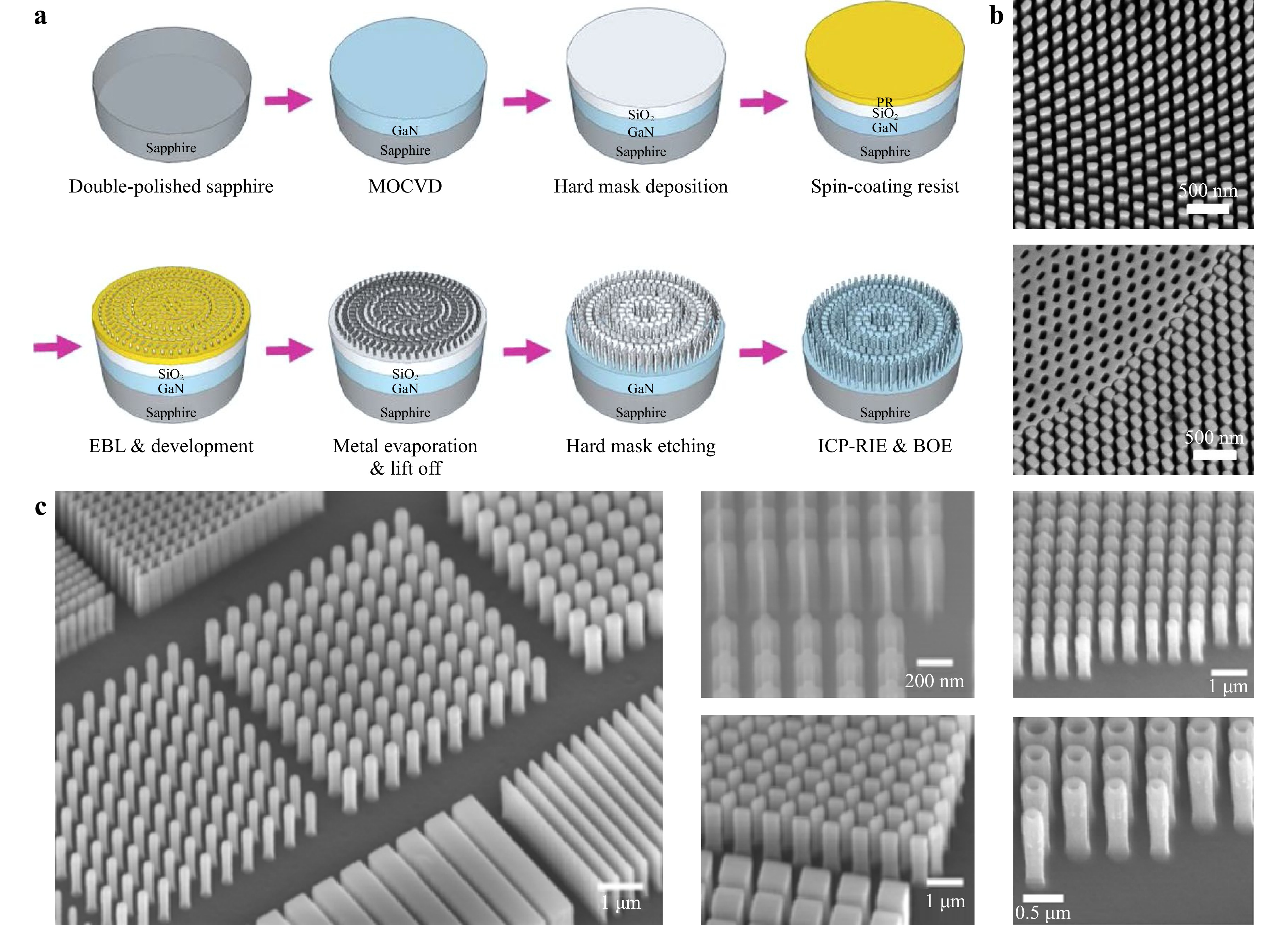
Fig. 1 Electron-beam lithography. a The process flow for the fabrication of GaN achromatic meta-lens working in the visible. b The corresponding SEM images of GaN nanopillars (top) and the inverse nanostructures (bottom)54. c The tilted view SEM images of the TiO2 nanostructures, including circular pillars, crosses, and rectangle pillars9.
Titanium dioxide (TiO2) is currently one of the most commonly used materials for metasurfaces in the visible and near-infrared bands, but most of the preparation of TiO2 metasurfaces still used the bottom-up atomic layer deposition (ALD) on EBL patterned resist, followed by dry etching the top TiO2 layer and removing the residual resist55,56. The height and aspect ratio of nanopillars prepared by this method are limited to 600 nm and 15, respectively. Despite the seemingly high aspect ratio given by this method, the allowed fabrication limit is only suitable for Huygens metasurface57,58 and propagation-based metasurface. A much higher aspect ratio is preferred for applications such as chromatic aberration elimination. Xiao et al. have redeveloped a more efficient top-down dry etching method for TiO29. Similar to the preparation process in Fig. 1a, the metasurface pattern is applied to the resist using EBL, and then the pattern is transferred to the Cr layer through the lift-off process. The dry etching method by RIE is used to obtain the TiO2 nanostructures array. As shown in Fig. 1c, the structure has almost vertical sidewalls with record-high aspect ratios of 37.5. This etching technology provides strong support for the large-scale and efficient production of TiO2-based meta-devices.
More complicated geometries can be realized by combining other techniques with the EBL process. Chen et al. developed a kind of metasurface based on TiO2 with inclined nanopillar distribution by combining EBL and RIE dry etching techniques59. The process flow is shown in Fig. 2a. EBL is still used to pattern the trapezoidal arrays in the resist, and the pattern is then transferred to the Cr layer through dry etch by ICP-RIE. In the RIE dry etching step, the etched sample is tilted and covered with Faraday cages to orient the plasma distribution on the sample surface. Fig. 2c shows the side-view and cross-sectional SEM images of the inclined metasurface. The use of adjustable tilt etching technology breaks the traditional mirror symmetry of metasurfaces, unleashing the flexible characteristics of metasurfaces, and providing innovative ideas for the development and application of meta-devices. 3D nanostructures are also possible with advanced dry etching technologies. An uniaxial isotropic metamaterial composed of 3D metallic split-ring resonators (SRRs) is experimentally demonstrated by EBL process, as given in Fig. 2d60. A layer of positive e-beam resist, PMMA, is spin-coated on the silicon substrate, followed by EBL process to define the ring pattern. Au/Ni double metal layers are deposited on the patterned sample. Additional Au/Ni are removed by the lift-off process. After dry etching the silicon substrate using CF4, the planar metal nanostructures are spontaneously folded by the higher tensile stress in the top Au layer than in the bottom Ni layer. The fabricated fourfold-symmetric SRRs are exhibited in Fig. 2e. The proposed metamaterial shows great potential in generating a bi-anisotropic response. These fabrication techniques also apply to other lithography methods for complex pattern creation.
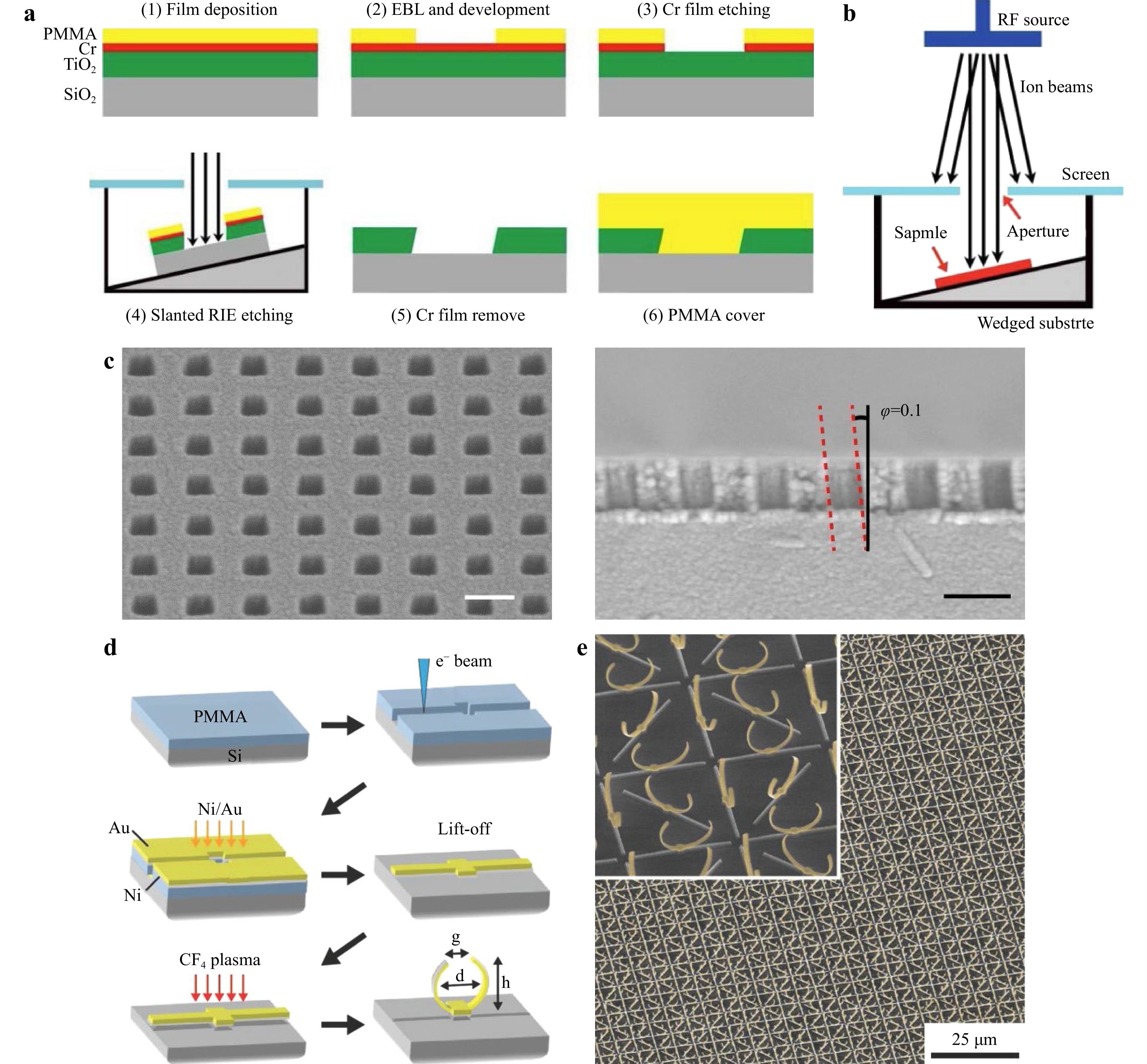
Fig. 2 Electron-beam lithography. a The process flow for the fabrication of inclined metasurface. b Schematic illustration of the slanted RIE system. c Side-view (left) and cross-sectional (right) scanning electron microscope images of inclined metasurface. Scale bar, 300 nm59. d The fabrication process for 3D SRR using EBL. e The SEM images of 3D SRRs with four-fold symmetry60.
EBL also acts as a one-step fabrication technique without further pattern transfer steps. Huang et al. experimentally demonstrated an all-dielectric metasurface supporting ultrahigh Q resonance61. In their design, a patterned resist, ZEP520, is directly utilized as the top perturbation structure, which avoids the etching steps and ensures a higher fabrication accuracy. However, unlike conventional photolithography, EBL is a pixel-by-pixel technology, which means EBL only writes a small pixel at a time. The high cost, long processing time, and highly stable requirements prevent EBL from large area and high-volume manufacturing. Owing to the electron scattering in the resist and substrate, the resolution of EBL is mainly determined by electron scattering instead of beam size of incident electrons62.
-
Instead of using electrons to expose the surface resist, focused ion beam (FIB) lithography applies heavy ion beams to bombard the sample surface, resulting in the direct removal of neutral and ionized atoms from the surface63. FIB provides a maskless one-step milling process with nanometer-scale precision. Through the combination of FIB with SEM to form the dual-beam system, direct imaging and analysis of the target sample can be realized.
Tseng et al. experimentally realized a 3D chiral metasurface by FIB adopting gallium ions64. As illustrated in Fig. 3a, the metasurface consists of an array of Archimedean spiral lines made of Si3N4/Au bilayer film. The Archimedean spiral patterns are obtained by one-step milling across both Si3N4 and Au thin film using FIB. Due to the stress and defects introduced in the milling process, the planar spiral lines stretch towards the out-of-plane direction and form the 3D ones. The top and tilted SEM images of fabricated spirals are shown in Fig. 3b. The linewidth of the spiral is 80 nm. Materials, film thickness, quality of the ion beams, and milling directions determine the final geometry of the 3D nanostructures. The experimental results show that the spirals have strong chiral dissymmetry over a broad infrared region and can be applied to chiral photomechanical sensors. The shape of 3D nanostructures can further be precisely manipulated by controlling the ion beam irradiation65.
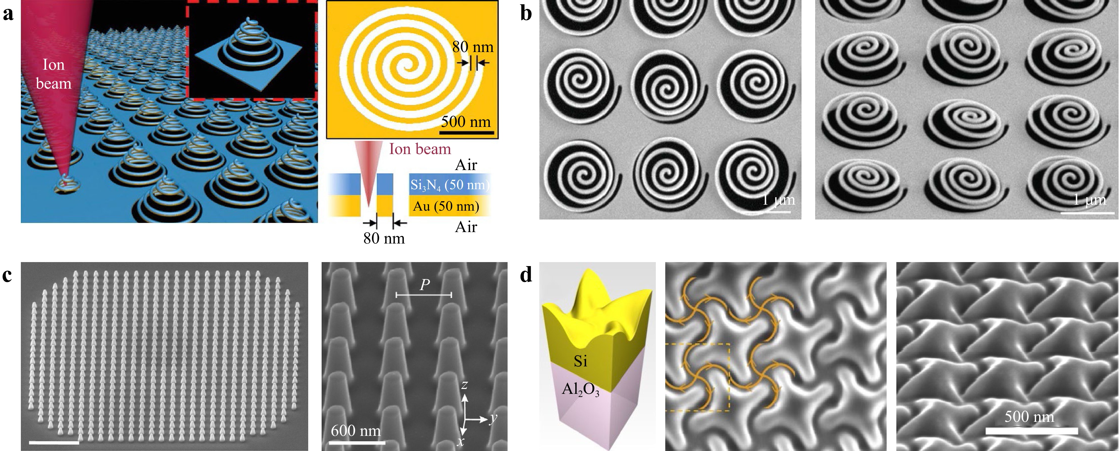
Fig. 3 Focused ion beam lithography. a Schematic of Archimedean spiral metasurface fabrication process by FIB. b The corresponding top (left panel) and tilted (right panel) SEM images of the fabricated metasurface64. c SEM images of LN maetasurface for second harmonic enhancement70. d Schematic configuration of the metasurface unit cell and the corresponding SEM images71.
FIB shows its great potential in etching difficult-to-etch materials. For example, lithium niobate (LN) is hard to etch and faces challenges in realizing vertical sidewalls and large etching depth66-69. Fig. 3c depicts the SEM images of an LN metasurface, which boosts the second harmonic in the visible region70. The LN thin film is milled directly by FIB. The side walls of LN nanopillars have an angle of 83.6°.
FIB is suitable for freeform surface patterning. Gorkunov et al. show a chiral metasurface on crystal silicon film fabricated by digitally controlled FIB71, as given in Fig. 3d. The SEM images show that, instead of flat patterns with vertical side walls, the meta-atoms have geometry with smoothly varying height and four-fold rotational symmetry. Gholipour et al. also adopted FIB in the fabrication of a perovskite metasurface72. FIB is a more flexible patterning method than EBL. However, it suffers from high costs and low throughput and cannot be applied to massive manufacturing. Ion doping, sample damage, and sample displacement during milling will degrade the performance of the fabricated samples.
-
Despite the high resolution of patterning with focus beams of particles, maskless fabrication techniques with flexibility, high throughput, and large-area fabrication are heavily desired. The direct application of laser into pattern writing provides a competitive solution.
Laser direct writing (LDW) lithography is a common technology adopted in mask writing in the semiconductor industry. As it is named, LDW applies laser to expose the photoresist directly. The exposure position is controlled by the moving stage. Zhang et al. demonstrated a plasmonic metasurface by LDW73. After the multiple depositions of gold, GST, and MgF2 films on the glass substrate, followed by spin-coating the photoresist, the laser beam writes on the top to define the geometry of the plasmonic nanoantenna. Fig. 4a shows the SEM image of the plasmonic metasurface. The metasurface achieves reconfigurable beam shaping within wavelengths ranging from 8.5 µm to 10.5 µm. Based on the LDW technique, an all-dielectric metasurface which produces polarization-sensitive optical vortices is also fabricated74. As given in Fig. 4b, Si nanorods with various geometric configurations are clearly observed. The expense for LDW technique is relatively low. Through the integration with other optical components, such as spatial light modulators (SLM), large-area manufacturing with high throughput is realized75,76. However, each sample must be prepared independently, making it difficult to carry out large-scale batch production.
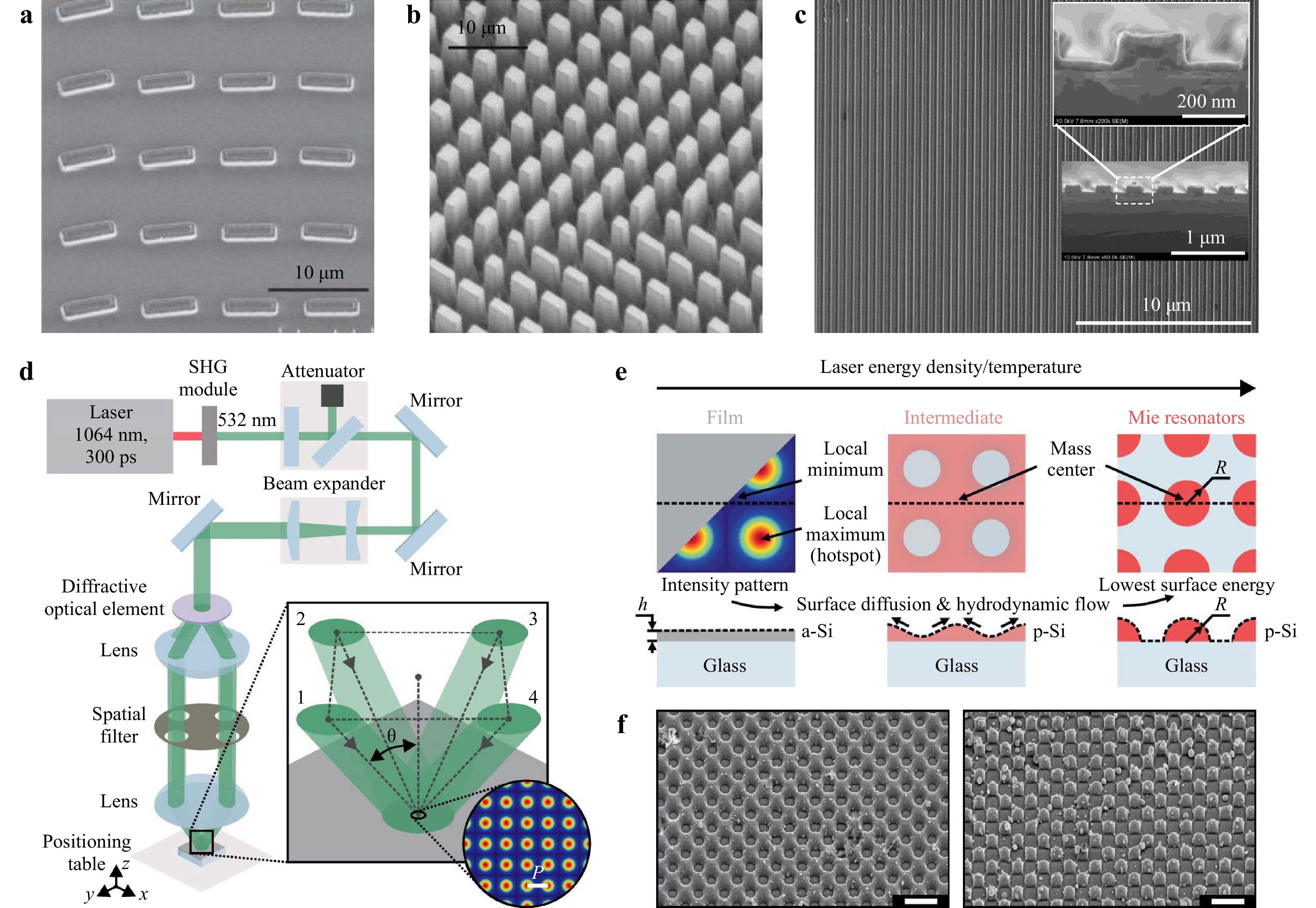
Fig. 4 Laser lithography. a SEM image of plasmonic metasurface fabricated by LDW73. b SEM image of the LDW-fabricated dielectric metasurface for optical vortices generation74. c SEM image of metasurface beam splitter manufactured by LIL77. d Schematic setup for four beam interference lithography. e, f Schematic of dewetting process for Mie resonator formation e and the corresponding SEM images f. Scale bar: 1 μm78.
Laser interference lithography (LIL) applies two or more coherent laser beams to create interference patterns with bright and dark regions. Such configurations ensure large-area periodic nanostructure manufacturing without the requirement for masks. Fig. 4c illustrates the SEM image of a metasurface beam splitter77. The periodic grating nanostructures are fabricated by LIL. More complicated structures other than periodic line shapes can be realized via LIL. Berzinš et al. experimentally show metasurface supporting Mie resonance using four-beam LIL78. The fabrication setup is given in Fig. 4d. A diffractive optical component is applied to split the incident light into four beams, which reach the sample surface after passing through the lens system. The four beams interfere and form a square-shaped lattice pattern. Single pulse laser is adopted to provide high power for melting the silicon thin film. As shown in Fig. 4e, the melted silicon diffuses to the dark region in the interference and reshapes to a hemi-spherical configuration to minimize the surface energy. The SEM images of the intermediate and final pattern of Si nano-resonator are depicted in Fig. 4f. Despite the fact that more complex configurations can be fabricated by applying more interference beams or controlling the beam intensity distribution79, LIL still cannot draw arbitrary or non-periodic patterns.
-
Photolithography, as the most widely used nanofabrication method in semiconductor industries, is compatible with the manufacturing of metasurfaces. This method uses light passing through the patterned photomask to transfer patterns to the photo-sensitive photoresist. An additional focusing lens can be applied to demagnify the feature size. Park et al. fabricated meta-lenses with a diameter of 10 mm on a 4-inch fused silica wafer using 248 nm KrF deep-ultraviolet (DUV) projection lithography80. Fig 5a depicts the fabrication process of the meta-lens. A layer of Chromium (Cr) is first deposited on the fused silica wafer, followed by DUV photoresist coating. After projecting the photoresist using DUV lithography, the patterns with 4:1 reduction of the feature size on the reticle are transferred to the resist layer. The Cr layer is dry etched to serve as a hard mask for silica etching. After removing the residual Cr, the silica nanopillars with a height of 2 µm are obtained. The optical image of the whole silica wafer and the SEM image of the corresponding nanostructures are shown in Fig. 5b. The tapered side wall is caused by plasma etching on the hard mask layer.
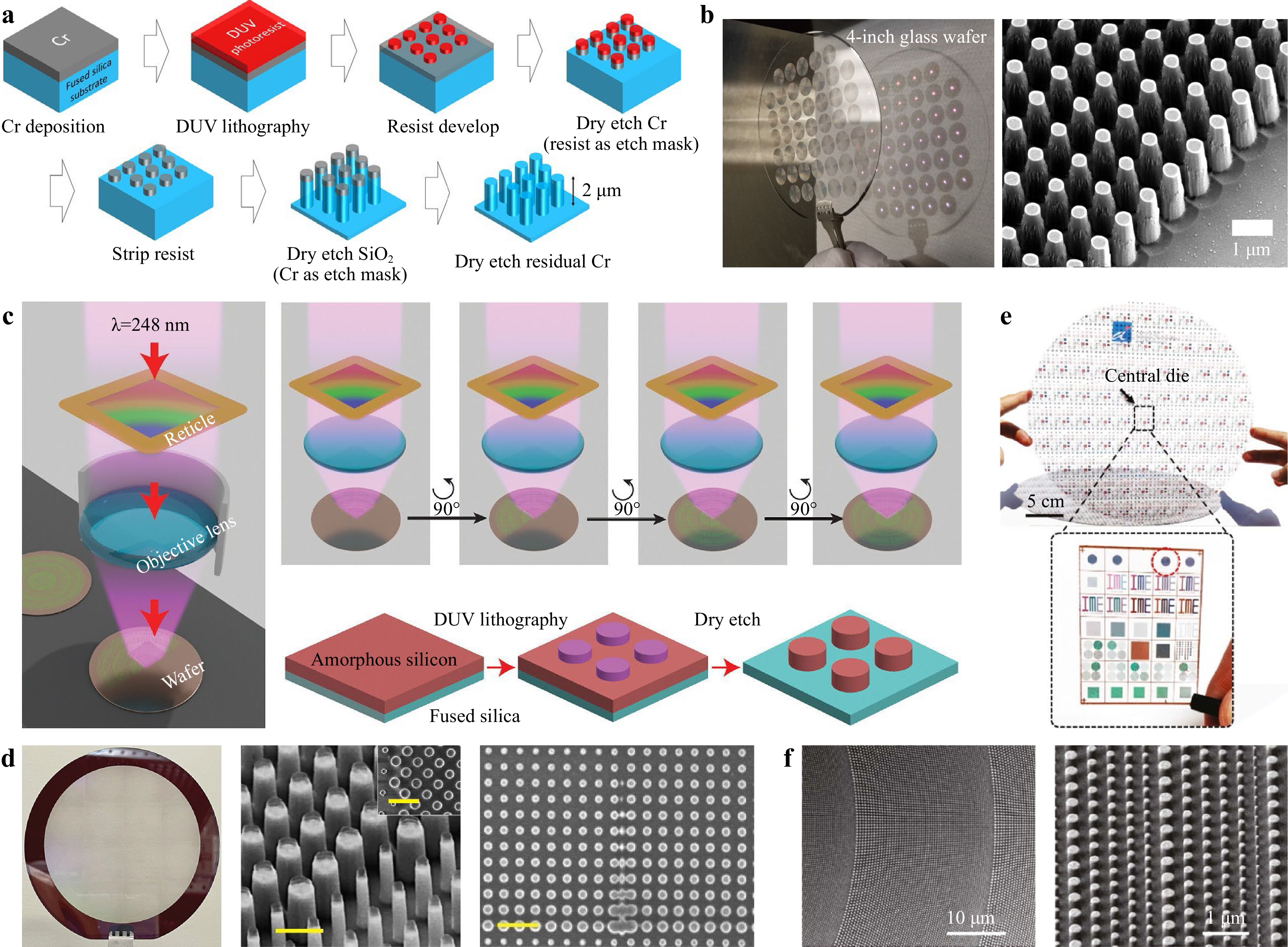
Fig. 5 Photolithography. a Process flow for fabricating large area all-glass meta-lens using DUV. b The corresponding optical image of meta-lenses on full 4-inch wafer and the SEM image of meta-lens80. c The fabrication process for 80 mm meta-lens with multiple exposures by DUV. d The optical image and the SEM images of the meta-lens81. Scale bar: 1 μm (middle), 2 μm (right). e Meta-lens and other meta-devices on 12-inch wafer manufactured by 193nm DUV. f The corresponding SEM images of the meta-lens82.
Photolithography has the potential for large-area fabrication with a high volume. Fig. 5c illustrates the process flow for wafer-scale meta-lens81. The meta-lens has a diameter of 80 mm, which exceeds the maximum exposure area for DUV. Multiple exposures are adopted to obtain the full meta-lens pattern. After dry etching through the silicon film, the meta-lens is fabricated. The photograph and SEM images of the wafer-scale meta-lens are given in Fig. 5d. The stitching errors are observed at the edges between the exposing areas, but the errors cause little effect on the optical performance of the meta-lens. Fig. 5e shows a 2 mm meta-lens made on a 12-inch wafer with the corresponding SEM images given in Fig. 5f82. 193 nm ArF DUV immersion lithography is adopted for pattern definition. Other meta-devices are also fabricated on the same wafer, as given in Fig. 5e. Photolithography provides a way for large-scale, massive production of meta-devices. However, DUV lithography has limited resolution, and a shorter wavelength is desired to make metasurface with finer feature sizes, such as extreme-ultraviolet (EUV) lithography, which increases the cost dramatically.
-
Nanoimprint lithography (NIL), unlike fabrication techniques mentioned previously, creates patterns on the imprint resist through mechanical deformation. A patterned master mold is contacted to the resist-coated substrate. By applying certain pressure with heat (Thermal-NIL) or UV light (UV-NIL), the resist is cured with an inverse pattern against the master mold. NIL provides an alternative high-volume fabrication method with cost efficiency. To extend the lifetime of master mold, additional soft molds are usually utilized as intermediate molds to transfer patterns to the resist.
Yoon et al. use one-step NIL to print the meta-lens working in the near-infrared region83. Thermally printable resin with Si nanoparticles embedded in it is utilized to increase the refractive index of the nanostructures, which enables a higher optical efficiency. The process flows are indicated in Fig. 6a. A soft mold with an inverse pattern is replicated from the master mold. The resin containing Si particles is coated on the soft mold. Then, the soft mold is pressed with the substrate under high temperature to cure the resin. After demolding the soft mold from the substrate, the original patterns on the mater mold are replicated to form the desired meta-lens. The SEM images of mater mold (left), soft mold (middle), and meta-lens (right) are depicted in Fig. 6b. The same idea for refractive index increasing in resin also applies to the visible spectrum, where TiO2 nanoparticles are mixed with resin84.
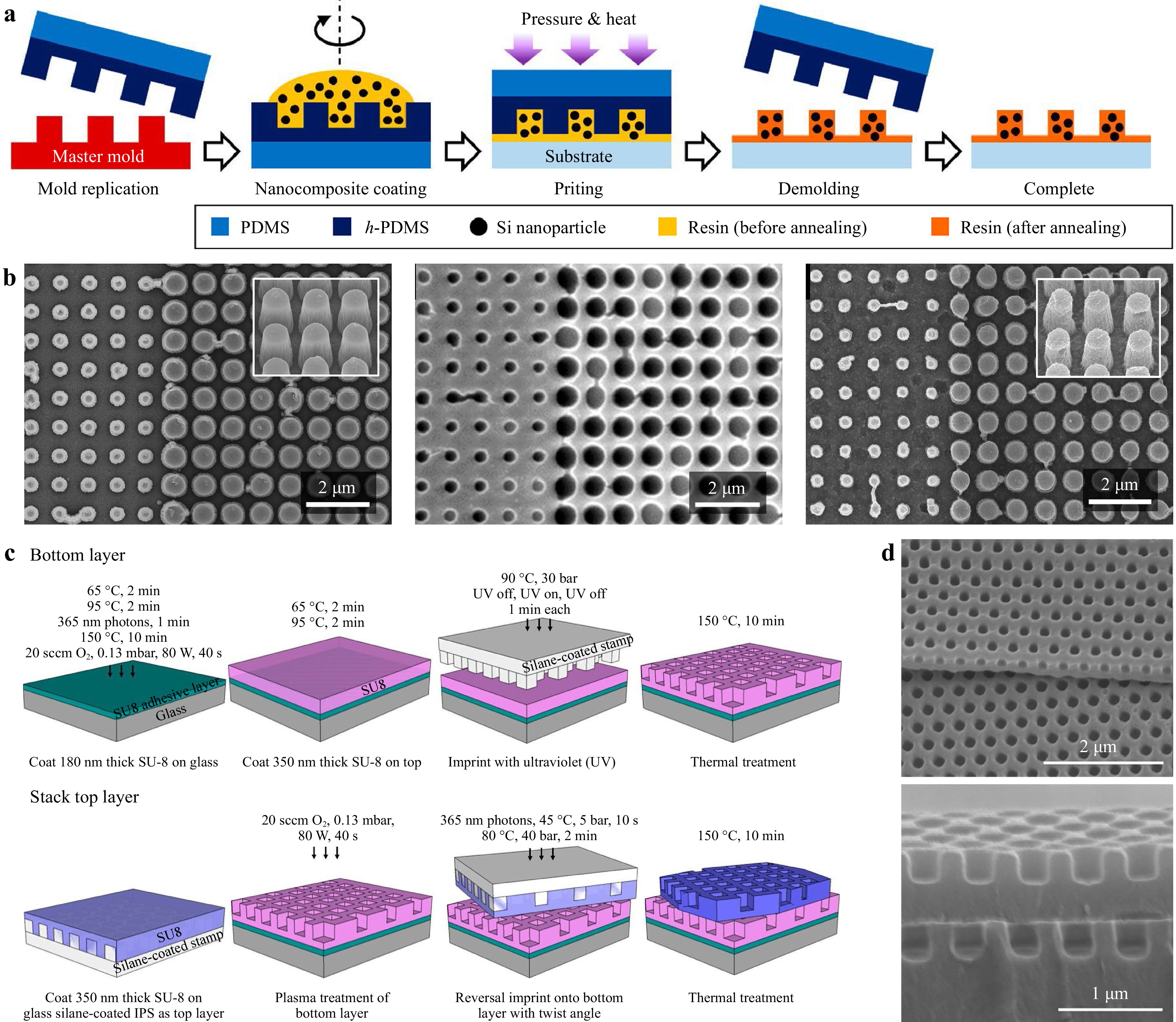
Fig. 6 Nanoimprint lithography. a The process flow for one-step NIL on meta-lens fabrication. b The SEM images of master mold (left), soft mold (middle), and fabricated meta-lens (right)83. c The NIL fabrication process for bilayer chiral meta-device. d The corresponding top and cross SEM images of bilayer meta-device85.
Chen et al. demonstrated a chiral bilayer meta-device using the printing method85. The process flow for fabricating bilayer patterns using NIL is shown in Fig. 6c. A layer of SU-8 is first deposited on the glass wafer and is cured to serve as adhesive layer. A second SU-8 layer is imprinted with UV light to replicate the inverse pattern from stamp. For the top layer, SU-8 is directly coated on the stamp with UV exposure to crosslink the SU-8. After inverting the coated stamp with a twisted angle, the SU-8 layer is detached to form the bilayer magic angle pattern. The top and cross-section SEM images are illustrated in Fig. 6d.
Einck et al. developed ink mixed with TiO2 nanoparticles for UV-NIL fabrication86. A meta-lens working in visible wavelengths is demonstrated to verify the performance of the TiO2 ink. Fig. 7 shows that a meta-atom with aspect ratio larger than 8 is experimentally achieved. Shrinkages on the nanostructures are found, which is due to the nature of sol-gel imprint materials. The shrinkages are reduced to about 10% by mixing the materials with solid TiO2 nanoparticles. A lifetime experiment is performed, which indicates that high feature fidelity is maintained for at least 15 imprints per stamp. NIL for large-area metasurface fabrication is also successfully demonstrated. Kim et al. reported cm-scale meta-lenses fabrication on 12-inch wafer by one-step NIL87. A thin layer of TiO2 is deposited to compensate for the low refractive index resin. NIL is also applied to pattern definition followed by etching process. A full-color reflective metasurface was realized with NIL only for resist patterning88. A silicon meta-lens using NIL only for etching mask definition was also performed89. NIL is a competitive candidate for high-resolution massive manufacturing. However, a high-resolution mold fabricated by other technology is required before processing the NIL fabrication. The low refractive index of imprinting resin/ink limits their light manipulation capabilities. This issue can be improved by adding high-index particles into the low-index resin83,86. The residual imprint layer is unavoidable and requires additional etching steps to remove it90. Lately, it was shown that the residual layer can also be utilized under specific designs. Instead of the tedious removal process of the residual layer, Kim et al. used the residual layer as an antireflection layer by optimizing its thickness91.
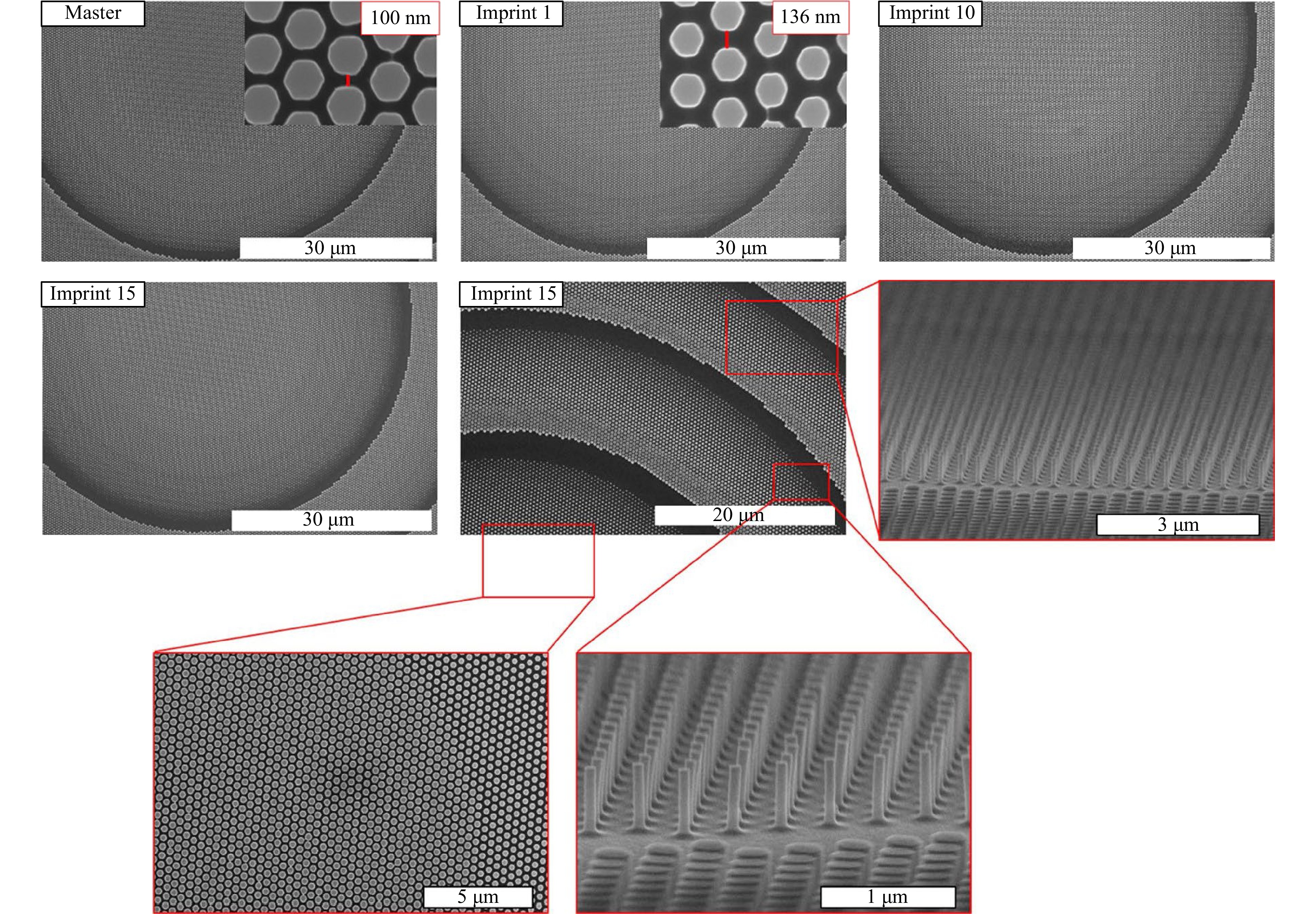
Fig. 7 Meta-devices fabricated by NIL. SEM images of multiple imprinted metasurfaces using the same mold86.
-
Self-assembly lithography is a simple nanofabrication method which controls the assembly of micro or nanoparticles to form the devices92. Nanosphere lithography (NSL) provides a low-cost solution to build hard mask consisting of self-assembled colloidal nanoparticles for the following pattern transfer steps. Polystyrene spheres (PS) are usually adopted as the nanospheres for a hard mask. Fig. 8a shows a PS sphere mask-making process with high monolayer quality93. PS mixed solution, which is typically available as an aqueous suspension, is injected into the substrate and forms PS monolayer at the air-liquid interface. To ensure the quality of PS monolayer, PS coated substrate is then inserted into DI water with PS staying on the air-water interface while the substrate is sunk to the bottom. Another hydrophilic substrate is applied to scoop the monolayer and form a high-quality monolayer mask on the substrate. The pattern is transferred to the substrate, followed by etching steps with PS as etching mask. The SEM images of the PS mask (top) and the fabricated sample (bottom) are shown in Fig. 8b.
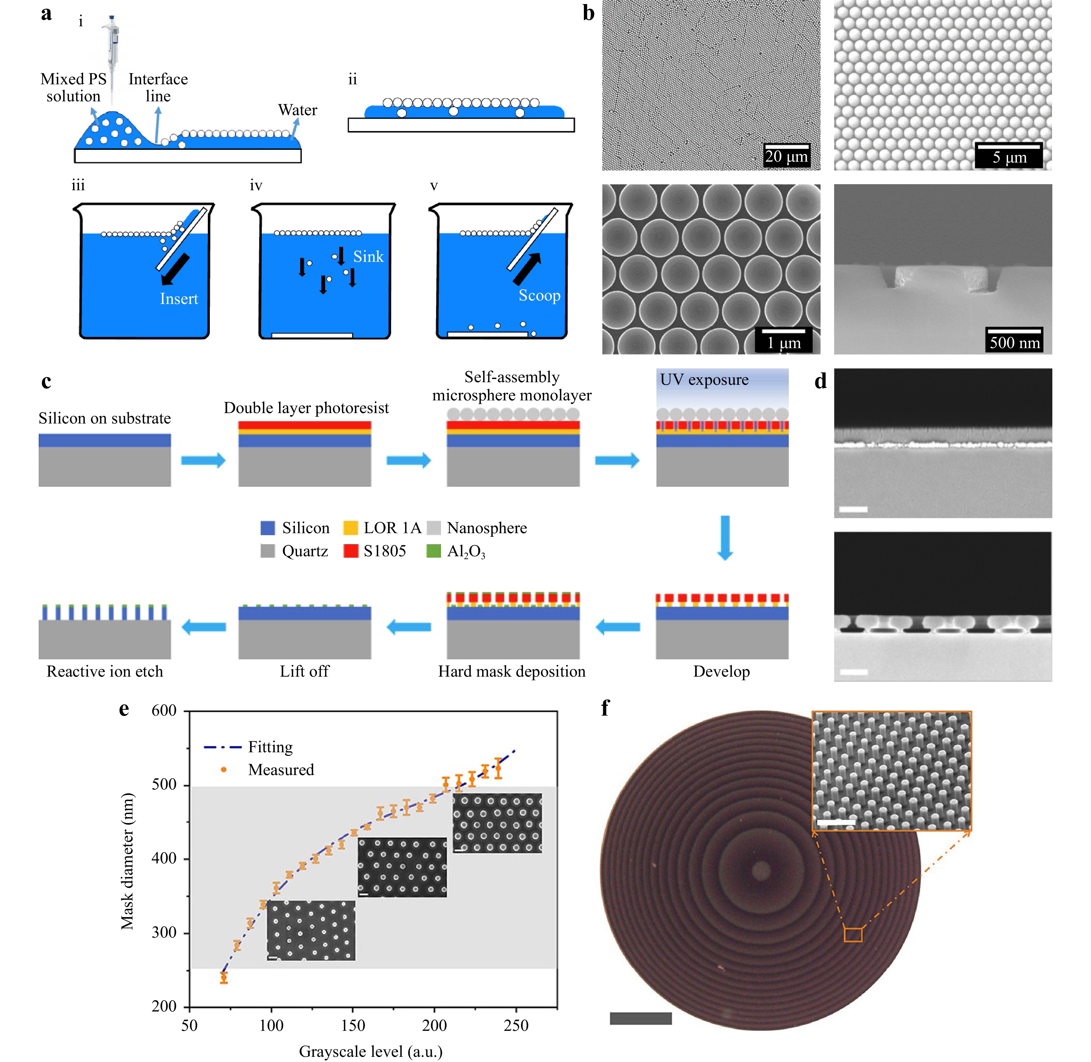
Fig. 8 Self-Assembly lithography. a Schematic diagram of mask making for self-assembly lithography. b SEM images of PS mask (upper) and the fabricated metasurface (bottom)93. c The fabrication process of the nanosphere self-assembly assisted grayscale lithography process step. d Cross-sectional SEM images of bilayer photoresist structure before lithography (upper) and after lithography (bottom). Scale bar: 400nm. e The diameter of the Al2O3 hard mask against the grayscale level of the pattern. Insets are SEM images of the hard masks fabricated under different exposure doses. Scale bar: 500 nm. f The corresponding optical image of the fabricated large-sized meta-lens. Scale bar: 200 μm. Inset is a tilted SEM image of the silicon nanopillars. Scale bar: 2.5 μm94.
Zheng et al. developed a novel manufacturing method based on the combination of nanosphere self-assembly and grayscale lithography94. Fig. 8c and Fig. 8d depict the fabrication process of the metasurface and the SEM images of patterned bilayer photoresist, respectively. By using self-assembled nanospheres on the surface of the photoresist as microlenses for grayscale lithography, the exposure area under each nanosphere can be precisely controlled by adjusting the exposure dose, thus obtaining masks with different sizes, as shown in Fig. 8e. Using this technology, fabrication of large-size meta-lenses and holograms is achieved. Fig. 8f shows the optical image of the meta-lens and the tilted SEM image of partial nanopillars.
The fabrication of complex geometry configurations is also possible using NSL95. Instead of using monolayer PS as common, PSs are stacked to form bilayer structures with moiré patterns. Then, the moiré pattern is transferred to the bottom substrate with PS bilayer as hard mask for gold deposition. This chiral metasurface has great potential for biochemical sensing. Tuning the deposition angle is another way to create various patterns on a fixed PS mask96. Nemiroski et al. demonstrated complex metasurface patterning by applying multiple-angle deposition97. Self-assembly lithography is a simple but effective method for large-scale meta-device fabrication. However, self-assembly lithography is only limited to homogenous patterns, and it is hard to avoid defects on the nanoparticle array.
-
Two-photon polymerization lithography (TPL) is a kind of additive manufacturing method that also belongs to the category of 3D printing. TPL provides rapid prototyping without restrictions on geometry configurations, which is suitable for prototype verification and research proposes. As depicted in Fig. 9a, a femtosecond laser is focused on the target resist. The exposed resin is cured only at the focal spot, where light intensity exceeds the curing threshold. The uncured resin is removed in the development process, leaving only the desired structures98. Liang et al. adopted TPL for fabricating anisotropic plasmonic metasurface working in the middle infrared region99. After curing the negative resist with femtosecond laser, a layer of gold is sputtered on the top to realize plasmonic metasurface, as shown in Fig. 9b. This metasurface achieves sharp resonance mode in reflection spectra, which significantly enhances the light-matter interaction. McLamb et al. presented a metasurface working in the infrared spectrum fabricated by TPL, which can be applied for chemical sensing and beam steering100. A meta-grating with free-form design was also fabricated through TPL, which acts as a polarization beam splitter in near-infrared101.
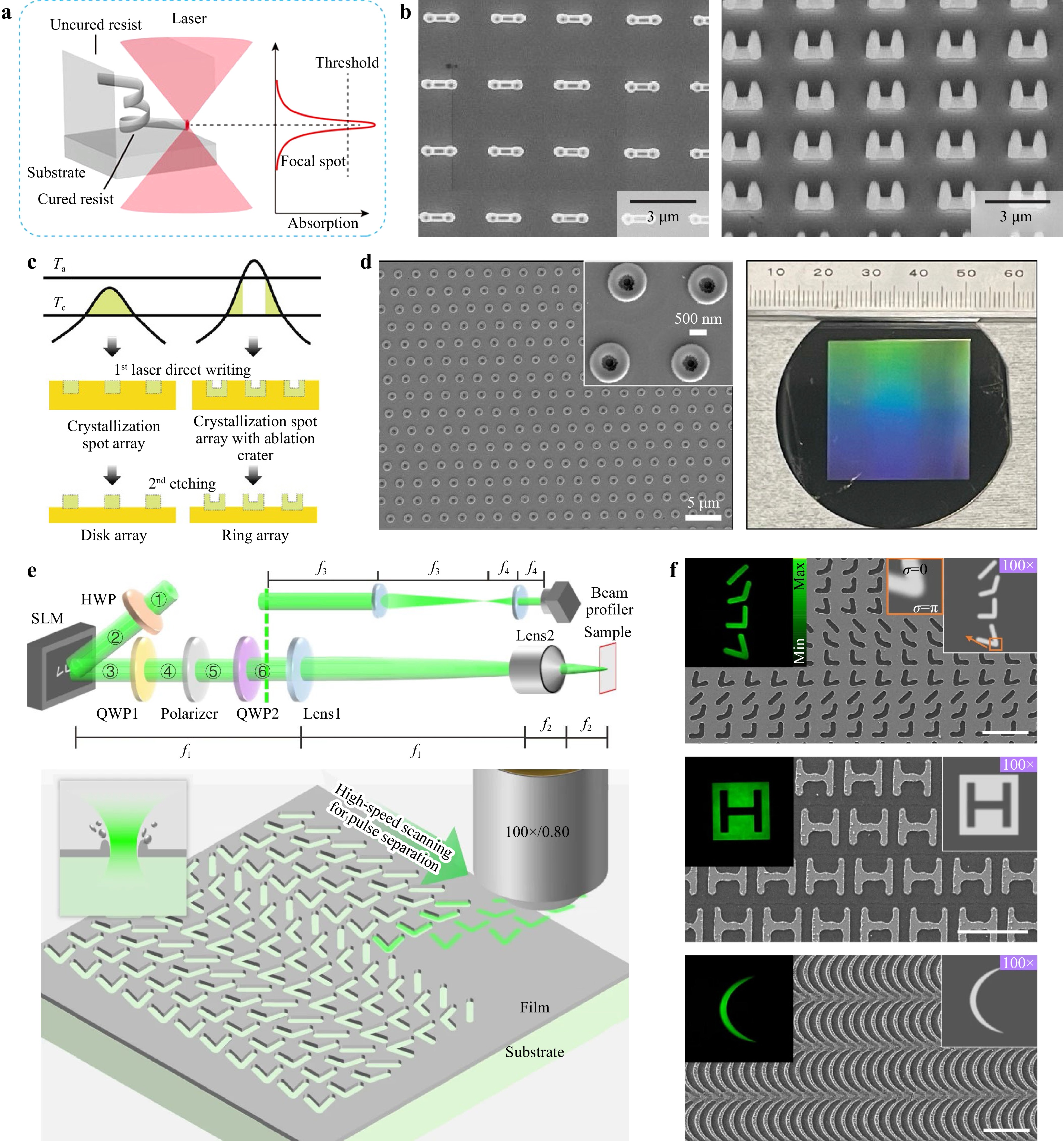
Fig. 9 Other meta-device fabrication techniques. a Schematic of two-photon polymerization98. b SEM images of plasmonic metasurface supporting bound states in the continuum99. c Laser ablation is used to create two different shapes in the GST material, and the metasurface is obtained through etching. d SEM images of the micro-ring structures and partial enlargement (left), as well as optical photos of the complete sample (right)102. e Schematic diagram of the optical path of the PPLL system and high-speed scanning and separated pulse ablation. f SEM images of fabricated structural arrays with sub-wavelength feature size and fine recast layers on boundaries. Scalar bars: 5 μm103.
-
Laser ablation is an alternative technology with low cost and high throughput for preparing large-area metasurfaces. The surface material is ablated or modified using a femtosecond laser system and subsequently etched to form a periodically arranged nanoarray. Yuan et al. take advantage of the different etching rates of the GST material in the amorphous phase and the laser-induced crystalline phase, as shown in Fig. 9c102. The disc and ring structures of the GST material are prepared through laser ablation, and the GST ring resonator cell is used to carry out centimeter-level large-area preparation, realizing tunable multiband meta-absorbers in the mid-infrared spectrum, as shown in Fig 9d. Huang et al. improved the laser ablation technology named patterned pulse laser lithography (PPLL), as shown in Fig. 9e103. Reflective SLM was used to phase-control the femtosecond laser for patterning, and the roughness of the pattern boundary was improved through polarization filtering. These result in the metasurface of arbitrary shapes and arrangements, as shown in Fig. 9f. This technology can work well in the infrared band, but achieving fine and highly uniform nanostructures suitable for the visible light band is still a big challenge.
-
In summary, the advanced nanofabrication technologies for meta-device fabrication are presented. The fabrication of meta-devices is a COMS-compatible process, indicating that a large number of fabrication techniques used in semiconductor industries can be applied to the fabrication of meta-devices. The fabrication techniques are divided into three categories: maskless lithography, masked lithography, and other techniques. The advantages and challenges of each method are discussed. Paying attention to the fabrication limit is crucial for meta-device realization. One should consider the fabrication resolution, allowed writing area, cost, fabrication time, and available materials to find the optimized method for performing the fabrication.
Through a decade of development, meta-devices have shown significant advancements in light manipulation compared to traditional optical devices. Novel functions and applications of meta-devices still remain to be explored. For instance, wide field-of-view meta-lenses have already been realized104, but a double-layer structure is required to achieve the wide field of view. A wide field of view realized by a monolayer meta-lens is still a challenge. Many efforts have been devoted to the study of nonlinear optics combined with metasurfaces, such as nonlinear generation105-109, nonlinear hologram110,111, and nonlinear imaging112. Expanding the nonlinear metasurface to vacuum ultraviolet or even extreme ultraviolet region is desired for light source miniaturization, nanofabrication113, biomedical technology114, and material analysis115. However, material loss is an unavoidable problem when moving to an extremely short wavelength range. Meta-devices for optical vortices are also realized, which are expected to be implemented on orbital angular momentum multiplexing communication systems116-119. Meta-devices for quantum state manipulation have also been reported120-122, proving the great potential of meta-devices in quantum computing and communication.
In the meantime, integration is the key step for metasurfaces to function as compact devices. For example, integrating metasurfaces on optical receivers and transmitters improves efficiency and enhances performance53,123,124; integrating metasurfaces with electrically tunable components (MEMS, liquid crystals and heaters) achieves tunable functions125-127; integrating metasurfaces with traditional refractive optical elements, planar waveguides, and optical fibers accurately controls wavefront and dispersion128-130. It is crucial to focus on improving the cost-effectiveness of integrated metasurfaces in future research.
To put forward the progress of meta-devices, improving existing technologies and developing novel fabrication methods with low cost, high throughput, uniformity, repeatability, large area, and high resolution is desired. As for the commercialization of meta-devices, masked lithography, such as DUV/EUV lithography and nanoimprint lithography, is a feasible solution. They are the widely used techniques for microelectronics fabrication with high throughput. However, as commercial lithography devices are mainly prepared for Si substrate, developing new progress flow to utilize high index material in the visible spectrum is necessary. The most important point is that nanofabrication should be combined with traditional optical element technology so that metasurfaces can start by replacing some traditional optical elements, gradually move from monolithic to integrated, and finally become advanced meta-devices. When large-scale manufacturing of meta-devices for commercial applications is required, the existing semiconductor manufacturing facilities (e.g., photolithography and nanoimprint lithography) can be adjusted to fit the requirements of meta-device fabrication without developing new equipment. Such compatibility significantly reduces the threshold of meta-device fabrication and facilitates the promotion of meta-devices and meta-optics.
-
Authors acknowledge the support from the University Grants Committee / Research Grants Council of the Hong Kong Special Administrative Region, China [Project No. AoE/P-502/20, CRF Project: C1015-21E; C5031-22G; and GRF Project: CityU15303521; CityU11305223; CityU11310522; CityU11300123], the Department of Science and Technology of Guangdong Province [Project No. 2020B1515120073], and City University of Hong Kong [Project No. 9380131, 9610628, and 7005867]. S.M. Xiao acknowledges financial support from National Key R&D Program of China (Grant Nos. 2021YFA1400802), the National Natural Science Foundation of China (Grant Nos. 62125501, and 6233000076), Fundamental Research Funds for the Central Universities (Grant No. 2022FRRK030004), and Shenzhen Fundamental Research Projects (Grant Nos. JCYJ20220818102218040).
Meta-device: advanced manufacturing
-
Borui Leng1,
 ,
, - Yao Zhang4,
- Din Ping Tsai1, 2, 3, *, ,
-
Shumin Xiao4, 5, *, ,
- Light: Advanced Manufacturing 5, Article number: (2024)
- Received: 30 September 2023
- Revised: 27 December 2023
- Accepted: 03 January 2024 Published online: 07 March 2024
doi: https://doi.org/10.37188/lam.2024.005
Abstract: Metasurfaces are one of the most promising devices to break through the limitations of bulky optical components. By offering a new method of light manipulation based on the light-matter interaction in subwavelength nanostructures, metasurfaces enable the efficient manipulation of the amplitude, phase, polarization, and frequency of light and derive a series of possibilities for important applications. However, one key challenge for the realization of applications for meta-devices is how to fabricate large-scale, uniform nanostructures with high resolution. In this review, we review the state-of-the-art nanofabrication techniques compatible with the manufacture of meta-devices. Maskless lithography, masked lithography, and other nanofabrication techniques are highlighted in detail. We also delve into the constraints and limitations of the current fabrication methods while providing some insights on solutions to overcome these challenges for advanced nanophotonic applications.
Research Summary
Advanced Manufacturing for metasurface realization
The advanced nanofabrication technologies ensure the realization of metasurfaces. This paper provides an overview of state-of-the-art metasurface fabrication technologies, including maskless lithography, masked lithography, and other nanofabrication techniques. Din Ping Tsai from City University of Hong Kong, China, Shumin Xiao from Harbin Institute of Technology, China, and their colleagues review the recent achievements of nanofabrication techniques that are compatible with the manufacture of metasurfaces. Lithography with or without the mask and other nanofabrication techniques for metasurface are discussed. This article reviews serval well-fabricated metasurface works and summarizes the strengths and limitations of the nanofabrication techniques.
Rights and permissions
Open Access This article is licensed under a Creative Commons Attribution 4.0 International License, which permits use, sharing, adaptation, distribution and reproduction in any medium or format, as long as you give appropriate credit to the original author(s) and the source, provide a link to the Creative Commons license, and indicate if changes were made. The images or other third party material in this article are included in the article′s Creative Commons license, unless indicated otherwise in a credit line to the material. If material is not included in the article′s Creative Commons license and your intended use is not permitted by statutory regulation or exceeds the permitted use, you will need to obtain permission directly from the copyright holder. To view a copy of this license, visit http://creativecommons.org/licenses/by/4.0/.

 DownLoad: