
Featured
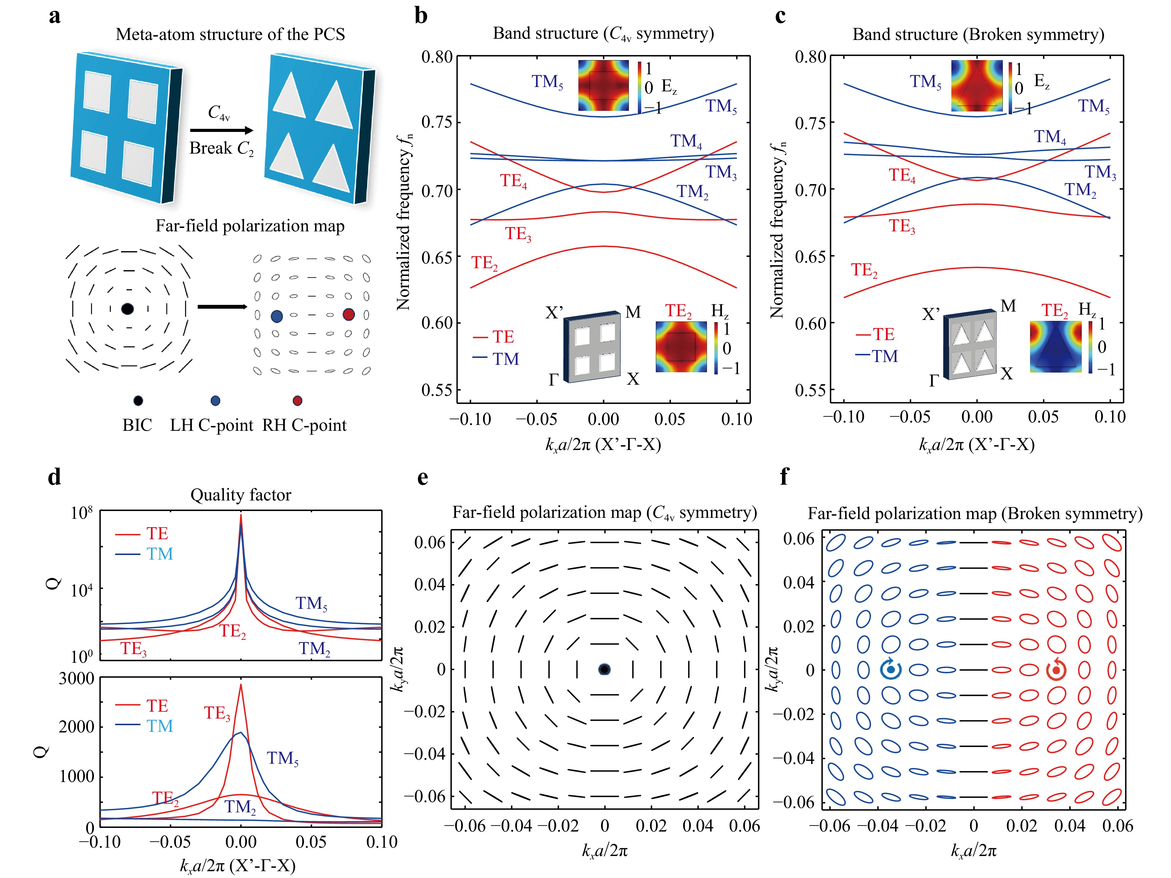
In photonic crystal slab (PCS) structures, the bound states in the continuum (BICs) and circularly polarised states (dubbed C-points) are critical topological polarisation singularities in momentum space that have garnered significant attention owing to their novel topological and optical properties. In this study, we engineered a novel PCS imager featuring two C-points with opposite chirality through symmetry breaking, resulting in maximal asymmetric transmission responses characterised by near-unity circular dichroism (CD) values. By harnessing the chiral selectivity of the C-points, a high-CD PCS imager can provide two sets of optical transfer functions (OTFs) to facilitate both edge detection and bright-field imaging. Notably, one set of OTFs was finely tuned to a Lorentzian line shape to achieve perfect edge detection. We developed a multifunctional imaging system by integrating a PCS imager into a traditional optical system. Both theoretical and experimental demonstrations confirmed that this system provides bright-field and edge-enhanced images with micrometer-scale resolution. Furthermore, these two independent functions can be easily switched by altering the circular polarisation state of the light source.


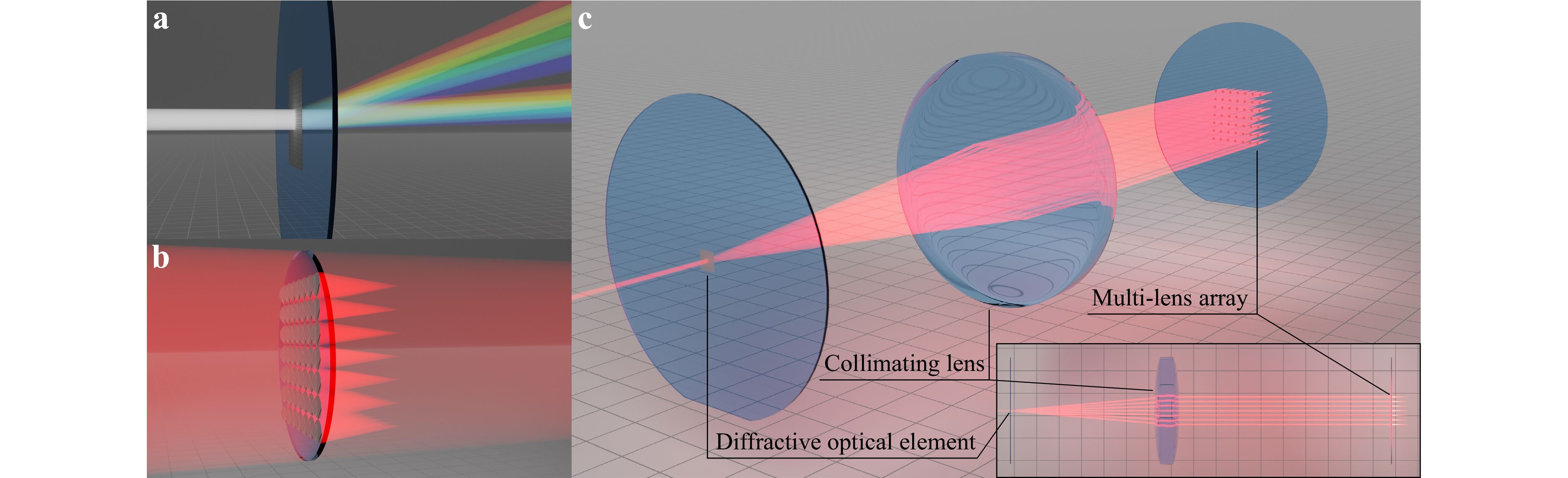
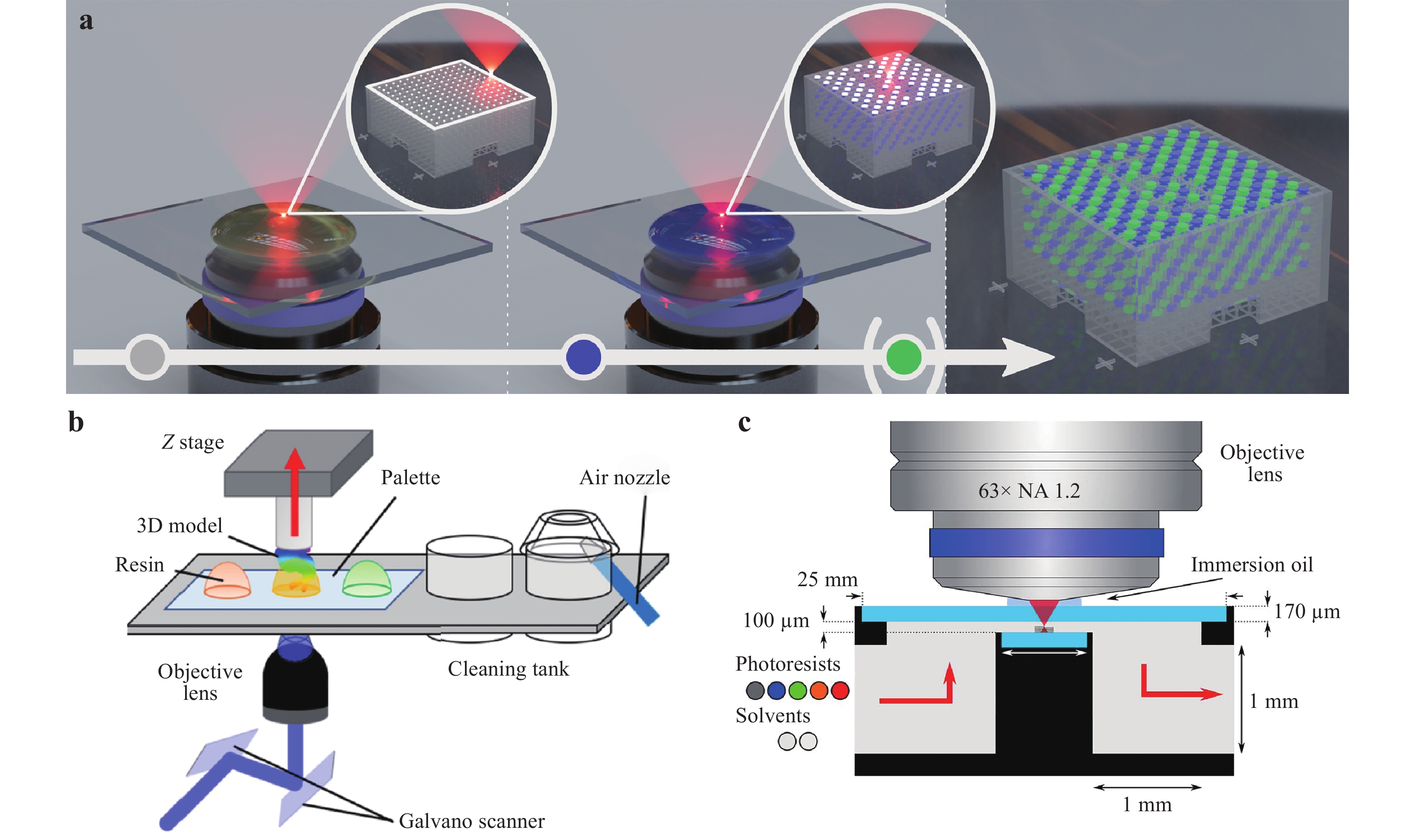
One of the challenges in the field of multi-photon 3D laser printing lies in further increasing the print speed in terms of voxels/s. Here, we present a setup based on a 7 × 7 focus array (rather than 3 × 3 in our previous work) and using a focus velocity of about 1 m/s (rather than 0.5 m/s in our previous work) at the diffraction limit (40×/NA1.4 microscope objective lens). Combined, this advance leads to a ten times increased print speed of about 108 voxels/s. We demonstrate polymer printing of a chiral metamaterial containing more than 1.7 × 10¹² voxels as well as millions of printed microparticles for potential pharmaceutical applications. The critical high-quality micro-optical components of the setup, namely a diffractive optical element generating the 7 × 7 beamlets and a 7 × 7 lens array, are manufactured by using a commercial two-photon grayscale 3D laser printer.

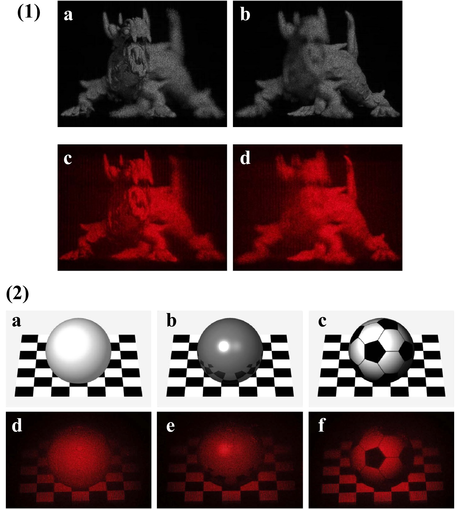
Holographic displays have the promise to be the ultimate 3D display technology, able to account for all visual cues. Recent advances in photonics and electronics gave rise to high-resolution holographic display prototypes, indicating that they may become widely available in the near future. One major challenge in driving those display systems is computational: computer generated holography (CGH) consists of numerically simulating diffraction, which is very computationally intensive. Our goal in this paper is to give a broad overview of the state-of-the-art in CGH. We make a classification of modern CGH algorithms, we describe different algorithmic CGH acceleration techniques, discuss the latest dedicated hardware solutions and indicate how to evaluate the perceptual quality of CGH. We summarize our findings, discuss remaining challenges and make projections on the future of CGH.


 Email
Email RSS
RSS