View by Category
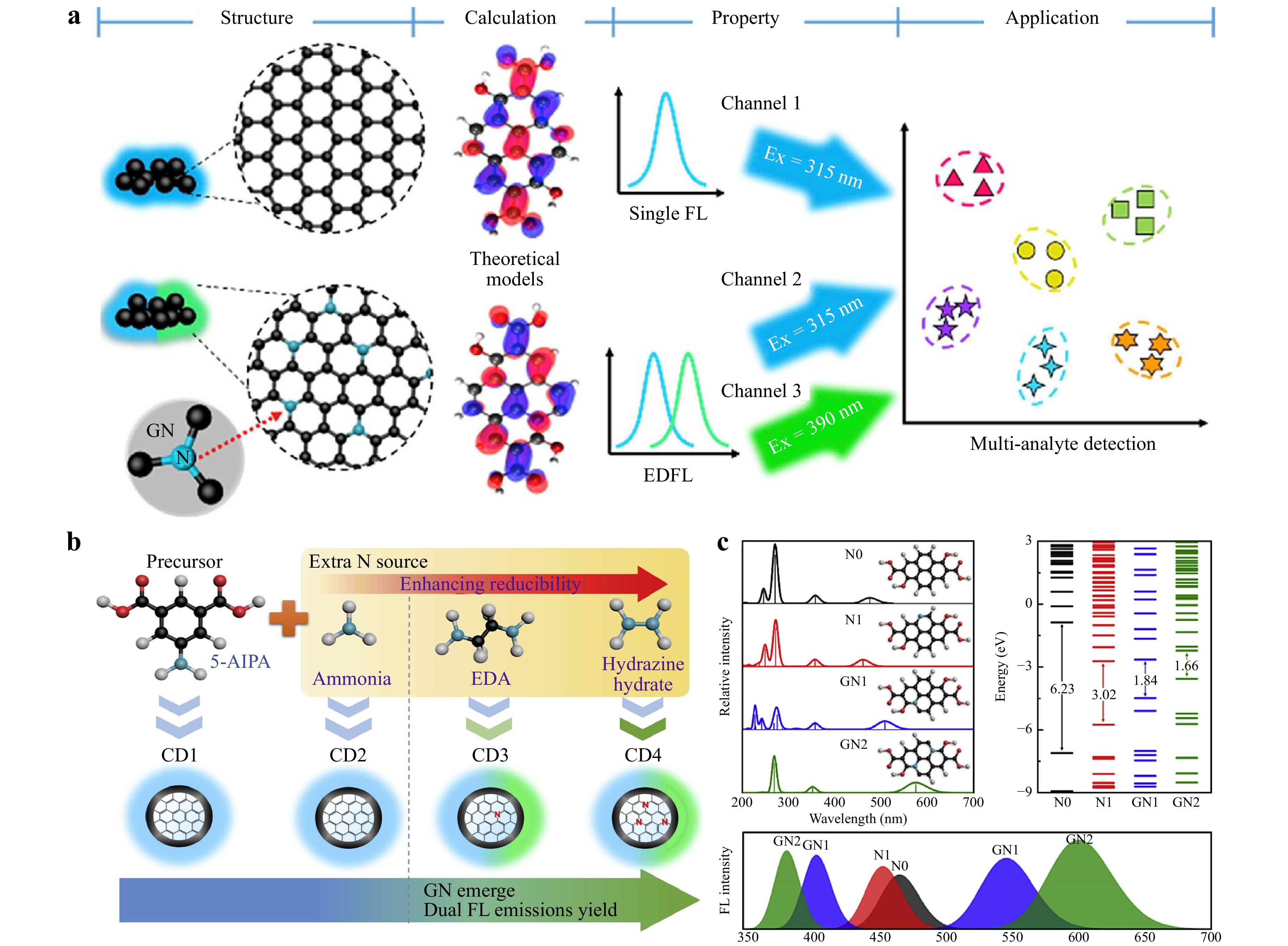
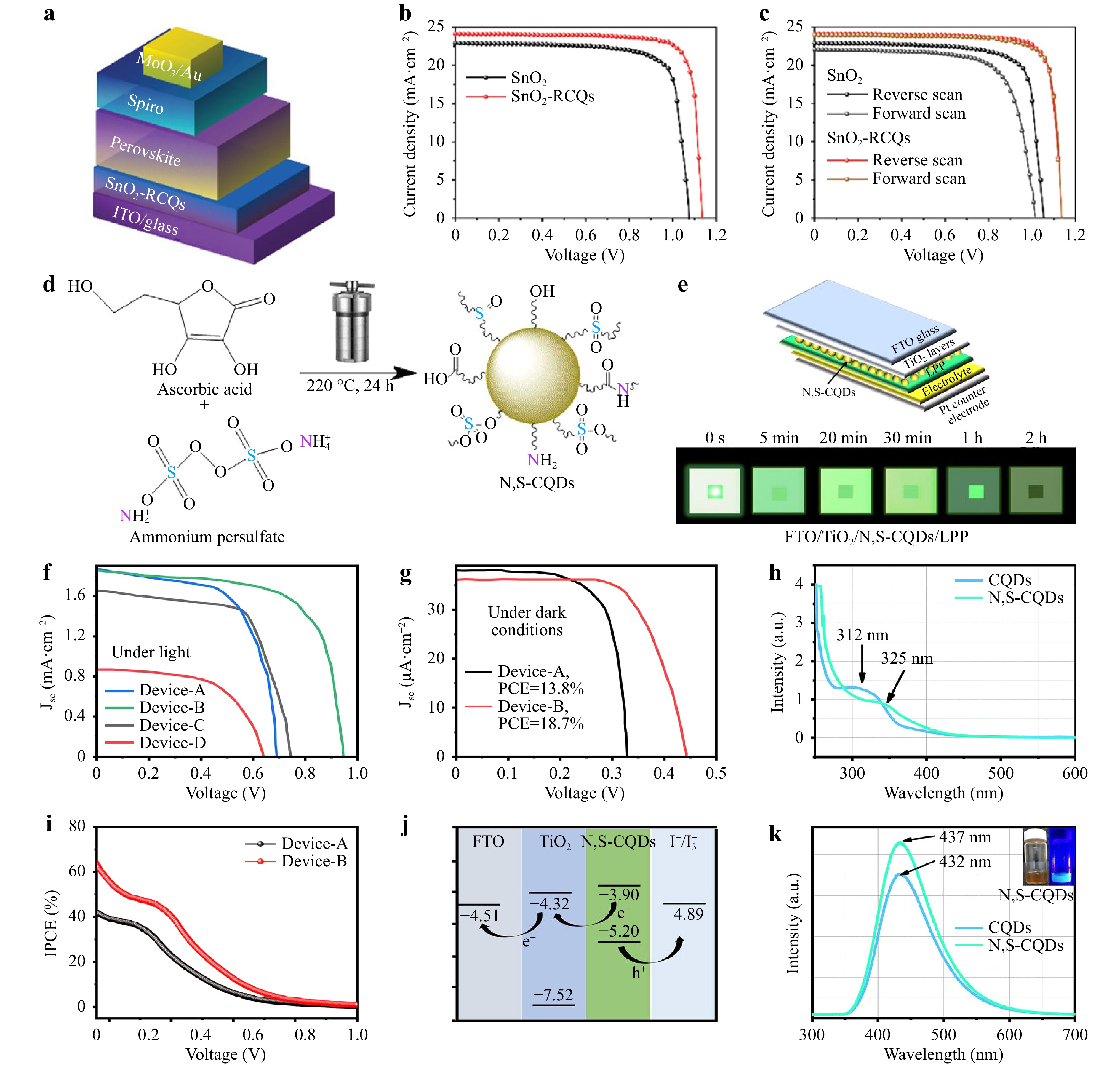
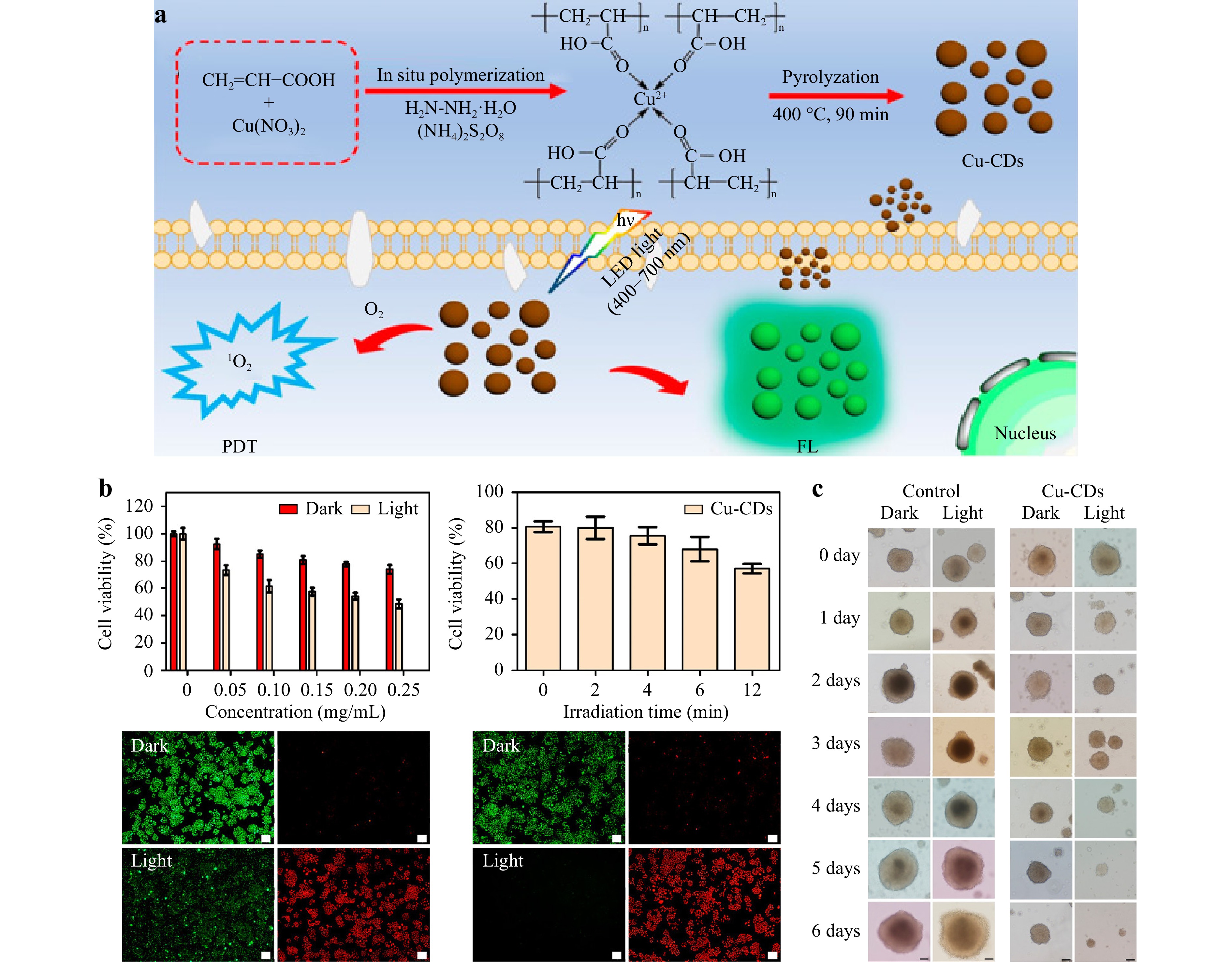
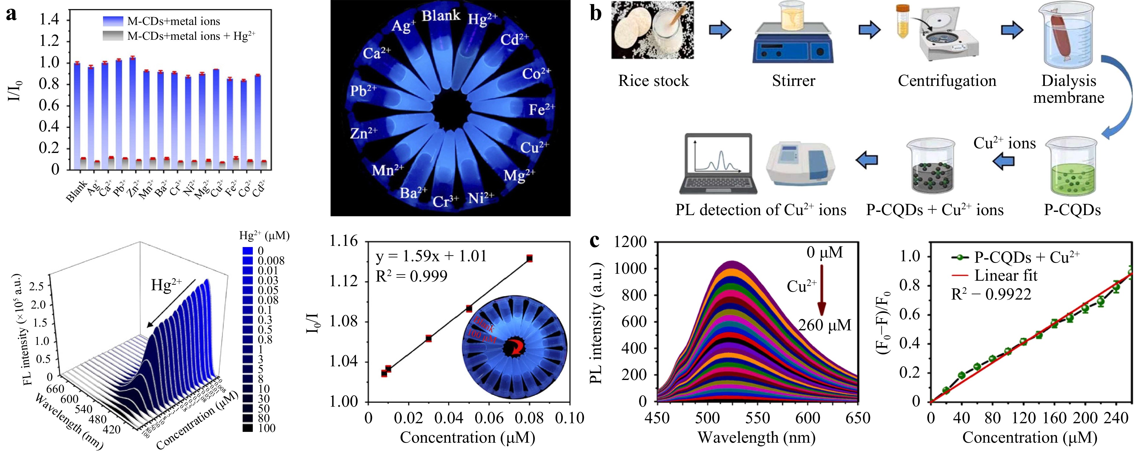
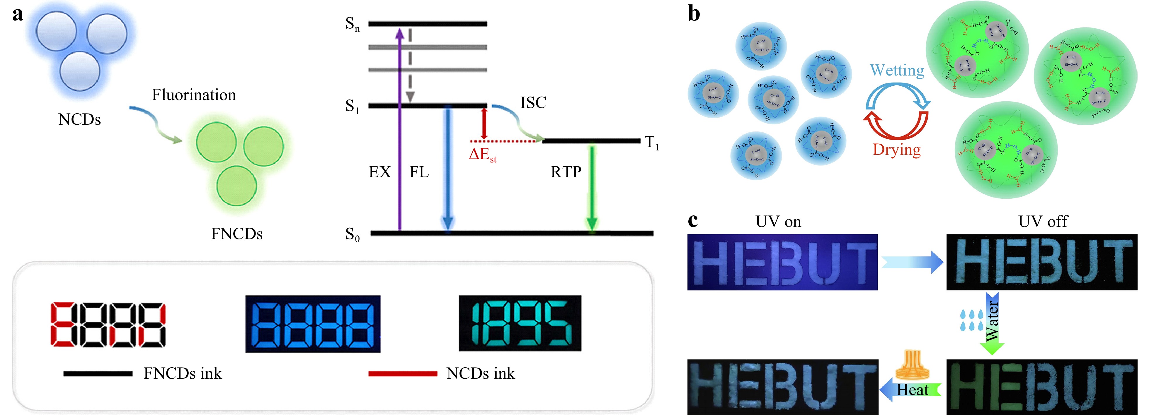
Carbon dots (CDs) have shown great potential for application in optoelectronics, owing to their merits of tunable fluorescence, biocompatibility, low toxicity, and solution processability. However, the intrinsic nature of CDs makes them prone to fluorescence quenching in the aggregated state. In addition, the emission peak width at half maximum of a single CD is usually greater than 60 nm, and the emission spectra may exhibit a multi-peak superposition state, resulting in poor monochromaticity. Further, the unsatisfactory quantum yield of CDs restricts their further application. Considering this, doping strategies have successfully improved the electrical, optical, and chemical properties of CDs. The intrinsic structure and electron distribution of CDs can be effectively adjusted by metal or nonmetal doping. Doping atoms generate n- or p-type charge carriers, changing the bandgap energy, and thereby improving the photophysical properties of the CDs. In this comprehensive review, we explore the intricate effects of various doping strategies on CDs and systematically categorize them. Notably, we elaborate on the diverse types of doped CDs and emphasize their photophysical properties, aiming to elucidate the fundamental mechanisms underlying the influence of doping on CD performance. Specifically, this review describes the extensive applications of doped carbon dots (X-CDs) in optoelectronic devices, information encryption, anti-counterfeiting measures, imaging techniques, and detection fields, to spur further X-CD exploration and application.
Dwell time plays a vital role in determining the accuracy and convergence of the computer-controlled optical surfacing process. However, optimizing dwell time presents a challenge due to its ill-posed nature, resulting in non-unique solutions. To address this issue, several well-known methods have emerged, including the iterative, Bayesian, Fourier transform, and matrix-form methods. Despite their independent development, these methods share common objectives, such as minimizing residual errors, ensuring dwell time's positivity and smoothness, minimizing total processing time, and enabling flexible dwell positions. This paper aims to comprehensively review the existing dwell time optimization methods, explore their interrelationships, provide insights for their effective implementations, evaluate their performances, and ultimately propose a unified dwell time optimization methodology.
Perovskite materials have become a popular research topic because of their unique optical and electrical properties, that enable extensive applications in information storage, lasers, anti-counterfeiting, and planar lenses. However, the success of the application depends on accomplishing high-precision and high-quality perovskite patterning technology. Numerous methods have been proposed for perovskite production, including, a femtosecond laser with an ultrashort pulse width and ultrahigh peak power with unique advantages such as high precision and efficiency, nonlinearity, and excellent material adaptability in perovskite material processing. Furthermore, femtosecond lasers can induce precipitation of perovskite inside glass/crystals, which markedly enhances the stability of perovskite materials and promotes their application and development in various fields. This review introduces perovskite precipitation and processing via femtosecond lasers. The methods involved and advantages of femtosecond-laser-induced perovskite precipitation and patterning are systematically summarized. The review also provides an outlook for further optimization and improvement of femtosecond laser preparation and processing methods for perovskites, which may offer significant support for future research and applications of perovskite materials.
Light microscopes are the most widely used devices in life and material sciences that allow the study of the interaction of light with matter at a resolution better than that of the naked eye. Conventional microscopes translate the spatial differences in the intensity of the reflected or transmitted light from an object to pixel brightness differences in the digital image. However, a phase microscope converts the spatial differences in the phase of the light from or through an object to differences in pixel brightness. Interference microscopy, a phase-based approach, has found application in various disciplines. While interferometry has brought nanometric axial resolution, the lateral resolution in quantitative phase microscopy (QPM) has still remained limited by diffraction, similar to other traditional microscopy systems. Enhancing the resolution has been the subject of intense investigation since the invention of the microscope in the 17th century. During the past decade, microsphere-assisted microscopy (MAM) has emerged as a simple and effective approach to enhance the resolution in light microscopy. MAM can be integrated with QPM for 3D label-free imaging with enhanced resolution. Here, we review the integration of microspheres with coherence scanning interference and digital holographic microscopies, discussing the associated open questions, challenges, and opportunities.
Metal halide perovskites have emerged as game-changing semiconductor materials in optoelectronics. As an efficient micro-/nano-manufacturing technology, direct laser writing (DLW) has been extensively used to fabricate patterns, micro/nanostructures, and pixel arrays on perovskites to promote their optoelectronic applications. Owing to the unique ionic properties and soft lattices of perovskites, DLW can introduce rich light–matter interactions, including laser ablation, crystallisation, ion migration, phase segregation, photoreaction, and other transitions, which enable diverse functionalities in addition to the intrinsic properties of perovskites. Based on their patterned structures, perovskites have numerous applications in displays, optical information encryption, solar cells, light-emitting diodes, lasers, photodetectors, and planar lenses, which are comprehensively discussed in this review. Finally, we discuss the challenges that must be addressed for the future development of this fascinating field.
- First
- Prev
- 1
- 2
- 3
- 4
- 5
- 6
- Next
- Last
- Total:6
- To
- Go