


-
The increasing demand for data storage systems, ranging from data centres to various smart devices, has led to an increasing need for higher-capacity, more compact memory devices. As the cell-to-cell distance has decreased to less than 10 nm, traditional two-dimensional (2D) scaling methods suffer from cell-to-cell interference and technical difficulties in fabrication processes1, 2. As an alternative approach, three-dimensional (3D) scaling has been proposed, and it has increased the number of transistors per area by overcoming the spatial limitations of traditional 2D devices3. Most notably, the storage capacity and energy efficiency of 3D NAND flash memory devices have been significantly improved by stacking memory cells vertically4, 5. Since the first launch of 3D NAND with 24 word line layers in 20136, the number of layers has been rapidly increasing, and 3D NAND with approximately 100 word line layers has recently been commercialised7. Recently developed 3D NAND flash memory has a storage density of 1 terabit per 180 mm2 footprint8. Driven by demands for more massive storage devices, the market size for 3D NAND is expected to grow exponentially from
$ \$ 9 billion in 2017 to$ \$ 100 billion by 20259.There are several different methods of fabricating 3D NAND10-13. Nevertheless, building multilayer structures by alternating layers of semiconductor materials in the initial fabrication process (Fig. 1a) is the same for all approaches. In the multilayer deposition process, residual stresses can occur owing to the different thermal expansion coefficients between the layers14. This results in undesirable thickness variations after the process is complete. Even small thickness variations in each layer can affect the circuit performance of the final product15, 16. Therefore, it is highly desirable to accurately assess the thickness of the stacked semiconductor layers.
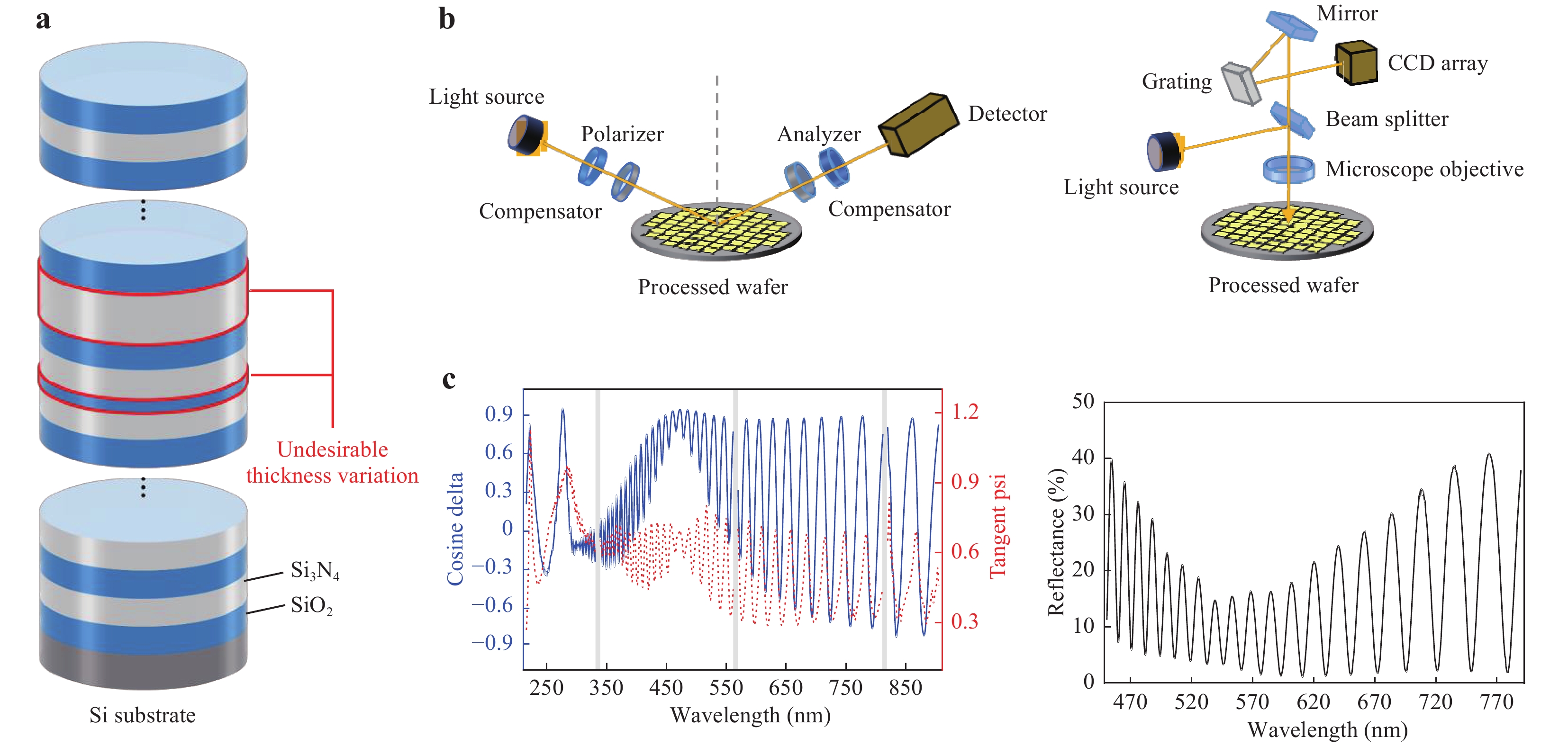
Fig. 1 Principles of the proposed multilayer thickness metrology method.
a Multilayer structure with alternating silicon oxide (blue) and silicon nitride (white) layers on a Si substrate. In the layer deposition process, undesirable thickness variations can occur. b Schematics of a typical spectroscopic ellipsometer (left) and reflectometer (right). c Examples of ellipsometric (left) and reflectance (right) measurement data. For the ellipsometric measurement data, the solid and dashed lines denote cosine-delta and tangent-psi, respectively. The grey areas indicate the unused spectral range, where the measurement errors between the instruments are large.To date, various measurement methods have been used in semiconductor device fabrication facilities to measure the nanoscale features of semiconductor devices17, 18. In particular, transmission electron microscopy (TEM) has been used to measure the thickness of semiconductor multilayer stacks19, 20. TEM has the advantage of high resolution and high magnification. However, owing to the destructive nature of the required wafer-cutting process, this technique cannot be used for total inspection. Another cross-sectional approach, for example, is to measure the cross-section of a multilayer by scatterometry with fast calculations using analytic approximation21. Interference microscopy can be used for the simultaneous characterisation of the multilayer thickness and the surface imaging22. Spectral ellipsometry, a non-destructive optical method, has been used for multilayer thickness characterisation23-26. However, as the number of layers increases, accurate thickness characterisation using spectroscopic ellipsometry becomes more difficult on account of errors in the measurement instruments and changes in the material properties of each layer under different fabrication conditions. Meanwhile, because the number of layers in 3D NAND will increase well above 200 layers in the near future, machine learning can be more effective for thickness characterisation of multilayer structures as compared to fitting methods27, 28. This is because the machine learning algorithm effectively learns the correlations between spectroscopic data and multilayer thickness without physical interpretation. Although thickness characterisation by artificial neural networks (ANNs) has been previously reported29-31, the characterisations were conducted only for a few (e.g. less than four) layers.
We herein demonstrate a non-destructive method for thickness characterisation of each layer in the > 200-layer semiconductor multilayer stacks that are used in commercial 3D NAND devices. By exploiting the structural similarity between semiconductor multilayer stacks and dielectric multilayer mirrors32, 33, various spectroscopic methods, including ellipsometric and reflectance measurements34, 35 (Fig. 1b), which are commonly used in dielectric mirror analysis, are employed. Based on the obtained spectroscopic data (Fig. 1c), machine learning is used to predict the thickness of each layer. From theoretical optical modelling (see ‘Materials and methods’ section), we exploit the well-known fact that the thickness of each layer affects the spectroscopic ellipsometric and reflectometric spectra. We can predict the thickness of each layer with an average root-mean-square error (RMSE) of approximately 1.6 Å (1.6 × 10⁻¹⁰ m, with ±0.2 Å standard deviation) for > 200-layer 3D semiconductor devices. In addition, using a machine learning model trained with simulated data, it is possible to correctly classify normal and outlier devices (e.g. a multilayer structure having a layer with > 30 Å deviation from the targeted layer thickness).
-
Accurate determination of layer-by-layer thickness for normal samples. The tested samples were multilayer semiconductor devices with alternating layers of oxide (SiO2) and nitride (Si3N4) on a silicon substrate. The total number of layers was approximately 200, with a total thickness of approximately 5.5 μm. Most layers consisted of quasi-periodic oxide/nitride layers with a thickness of 200 Å-330 Å, except for several top and bottom layers with a thickness of 100 Å-1,600 Å. For multilayer thickness prediction, ellipsometric data of 148 normal samples were used. For an outlier detection test, reflectance data of 45 normal samples and three outlier samples were used. Commercial ellipsometers and reflectometers (Atlas XP+, Nanometrics, Inc.), which were installed in the production lines of the 3D devices characterised in this work, were used to obtain the spectroscopic data. The ellipsometric data (psi and delta) were measured at an incident angle of 65° for a spectral range of 216-905 nm (Fig. 1c). Psi and delta were measured at 991 different wavelengths. In total, each sample had 1982 (= 991 × 2) measured psi and delta values. The reflectance was measured at an incident angle of 0° for a spectral range of 450-790 nm (Fig. 1c). The reflectance was measured at 741 different wavelengths.
After the spectroscopic measurements were conducted, each wafer was cut, and its cross-section was imaged by TEM. The TEM images were used as a reference for evaluating the accuracy of the proposed method. From the TEM images we determined that, even for the normal samples, the actual layer thickness could vary by up to approximately 20-30 Å from the target thickness, which corresponded to approximately 10-15% errors in the fabrication. The standard deviation of each layer thickness was in the range of approximately 3-11 Å (see Fig. 2a and 2b for the distributions of oxide and nitride layers, respectively).
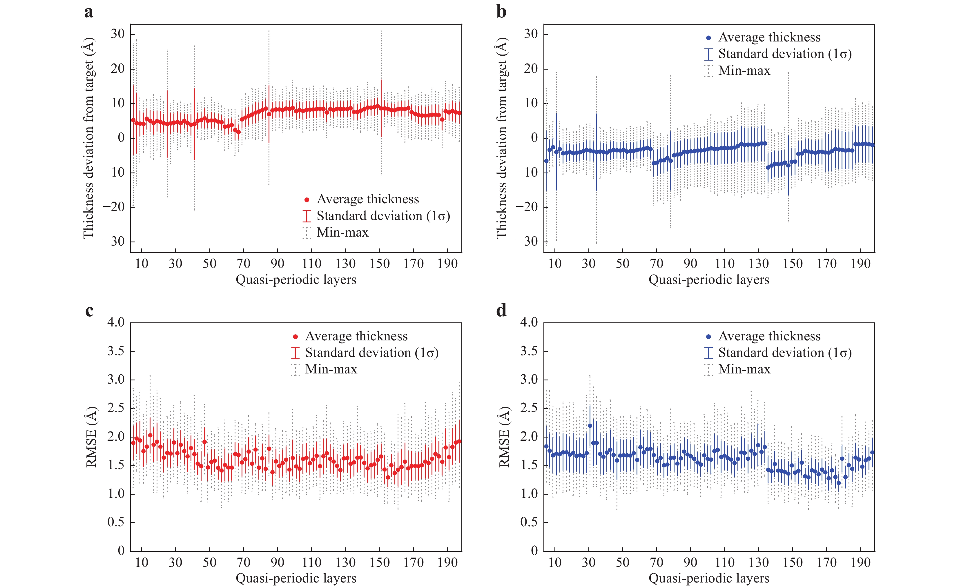
Fig. 2 Layer thickness distribution and prediction RMSE results.
a Thickness deviation from the design target for each oxide layer for 148 samples (determined by TEM images). b Thickness deviation from the design target for each nitride layer for 148 samples (determined by TEM images). c Prediction RMSE for quasi-periodic oxide layers. For each layer, the distribution of RMSE between the actual thickness and the predicted thickness for 23 test samples over 100 repetitions of random data splits is plotted with error bars. The average RMSE (red circles) occurs in the range of ~1.3-2.0 Å. d Prediction RMSE for quasi-periodic nitride layers. The average RMSE (blue circles) lies in the range of ~1.2-2.2 Å.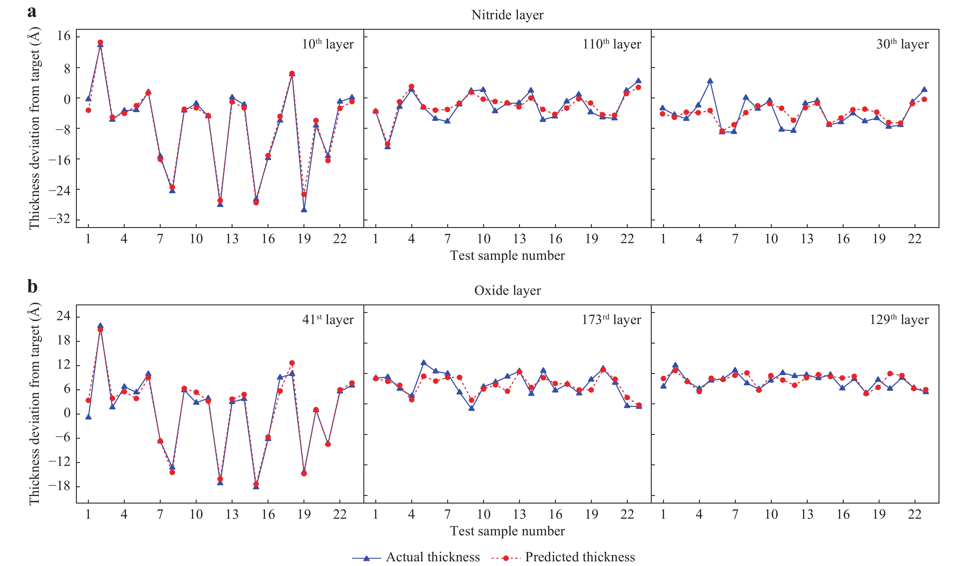
Fig. 3 Thickness prediction results for the 23 test samples.
Comparison between the actual (blue triangles) and predicted (red circles) thicknesses of a nitride layers (10th, 110th and 30th layers, showing the best, average, and worst agreement, respectively) and b oxide layers (41st, 173rd and 129th, showing the best, the average, and the worst agreement, respectively) for the 23 test samples.To determine the thickness of each layer from the measured spectral data, machine learning was used. For the machine learning model, spectral data and layer thicknesses were used as inputs and outputs, respectively. A total of 148 normal samples were randomly split into a training set of 125 samples and a test set of 23 samples. Owing to the limited number of available samples with TEM data, the number of training samples was increased to 5,000 by data augmentation based on noise injection methods (see ‘Materials and methods’ section). We used various machine learning models, such as support vector regression, linear regression models, and artificial neural networks. To evaluate the models, we implemented a five-fold cross-validation test. The linear regression model showed the best performance. Because the initial random split of 148 samples could reflect a biased result, we randomly split the dataset into 100 different combinations of training and test sets and trained the linear regression model on each training set (see Fig. S1). Finally, we applied the trained model to each test set.
Fig. 2a and 2b show the actual thickness distributions of 195 quasi-periodic layers for 148 normal samples (determined by the TEM images). After the deposition process, the oxide layer thickness tended to increase by approximately 7 Å, and the nitride layer thickness tended to decrease by approximately 4 Å from the original design target. The peak-to-peak distribution (grey bars in Fig. 2a, b of each layer thickness ranged from 10 Å to 50 Å. The standard deviation of the actual thickness (red and blue bars in Fig. 2a, b) was approximately 3-5 Å in most layers, while deviations of up to approximately 11 Å were also observed in some layers. Fig. 2c and 2d show the distributions of the RMSE of each layer thickness (i.e. the RMSE between the predicted layer thickness and the actual layer thickness determined by spectral data-driven machine learning and TEM imaging, respectively) for 23 test samples over 100 repetitions of random data splits. This result shows that our spectral measurement-based machine learning method achieved an average prediction RMSE of approximately 1.6 Å for each layer (red and blue circles for oxide and nitride layers, respectively).
To demonstrate the effectiveness of the proposed method for prediction, Fig. 3 presents a comparison between the actual thickness (determined by the TEM images) and the predicted thickness of several nitride and oxide layers (selected from the bottom, middle, and top parts of the multilayer structure) in the 23 test samples. The predicted thickness aligns well with the actual thickness, regardless of the material or layer position used, with an average prediction RMSE of approximately 1.6 Å.
To evaluate the correlation between the predicted and actual layer thicknesses, the R-squared value was calculated for each layer. Fig. 4a and 4b show the distribution of the R-squared values for each of the oxide and nitride layers, respectively. As shown in Fig. 4a, the highest and lowest R-squared values are 0.97 (41st layer, denoted by (i)) and 0.24 (35th layer, denoted by (ii)), respectively. As shown in Fig. 4c, for both the 41st and 35th layers, the predicted thickness (denoted by circles) is consistent with the actual thickness (denoted by triangles) with an RMSE of approximately 1.6 Å. Thus, the resulting R-squared value for the 35th layer is much lower than that of the 41st layer because the actual thickness distribution is much narrower (2.1 Å and 10.3 Å RMS distributions for the 35th and 41st layers, respectively). As shown in Fig. 4d, even though the actual total layer thickness is widely distributed from −400 to +900 Å from the design target, the predicted total thickness, which is the sum of all predicted layer thicknesses, has a high correlation (R-squared = 0.93) with the actual total thickness.
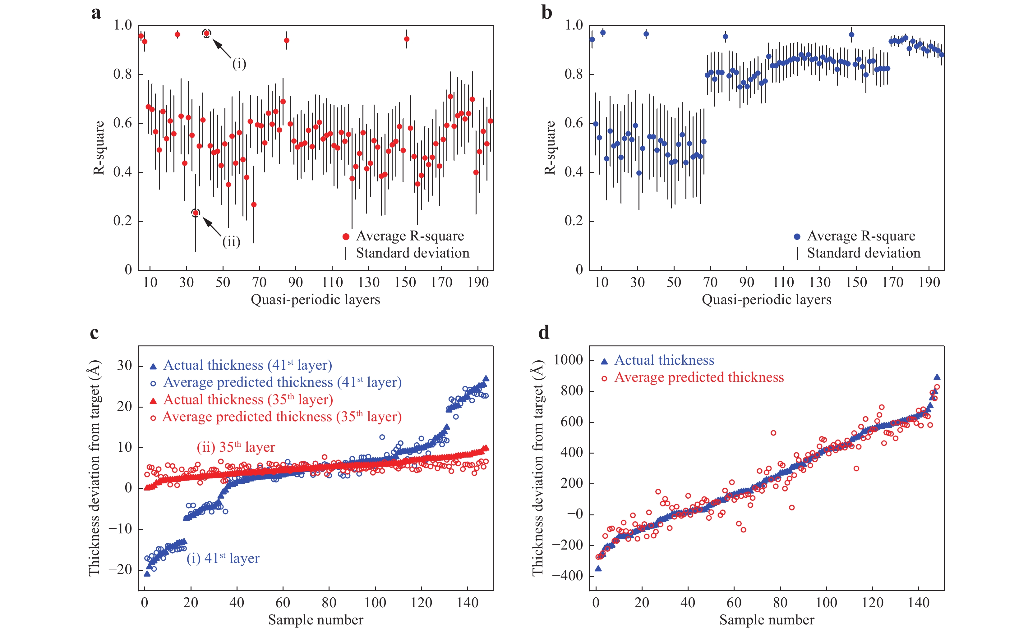
Fig. 4 Prediction correlation test results.
a The distribution of R-squared value for each oxide layer. The R-squared values for each layer are calculated for the 23 test samples averaged over 100 repetitions of random data splits. The highest R-squared value is denoted by (i); the lowest R-squared value is denoted by (ii). b Distribution of the R-squared value for each nitride layer. c Comparison of the actual layer thicknesses (blue triangles for (i) and red triangles for (ii)) for 148 samples and the corresponding predicted thicknesses (blue circles for (i) and red circles for (ii)) averaged over 100 repetitions of random data splits. Since the prediction RMSE is almost the same for all layers (see Fig. 2c, d), a narrower thickness distribution case leads to lower R-squared values. d Comparison of the actual total layer thicknesses (red triangles) for 148 samples and the corresponding predicted total layer thicknesses (blue circles) averaged over 100 repetitions of random data splits, with an R-squared value of 0.93.It is noteworthy that the number of training samples could be reduced at the expense of slightly degraded prediction performance. Figure S2 shows the average RMSE of each layer according to the number of training samples used for thickness characterisation of the > 200-layer structure. For example, when using 25 and 75 training samples (instead of 125), the RMSEs for the test set remain ~2.1 Å and ~1.75 Å, respectively. In addition, to investigate the applicability of our method, we applied our method to different multilayer oxide/nitride structures with ~65, ~110, and ~130 layers. As summarised in Table S1, 1.4-1.7 Å level RMSEs (over 100 repetitions of random data splits) could be obtained for each case when > 60 samples for training were used.
Outlier device detection using simulated data. In addition to the accurate determination of the multilayer thickness under normal fabrication conditions (as shown in Figs. 2-4), which is helpful for controlling etching and deposition processes, we developed another machine learning model that can detect outliers when layer thicknesses significantly vary (e.g. by more than 30 Å) from the design target. To distinguish outlier cases from normal cases, both normal and outlier samples are required to train the machine learning model. However, because it is impossible to fabricate all possible outlier samples for this training, we used a large number of simulated spectral data for more effective and economical training. The measured reflectance showed reasonable agreement with the simulated data. Therefore, reflectance data were used for the outlier detection models. We first generated 1,000 simulated data with a wide range of thickness distributions as outlier cases. We also generated 1,800 augmented data (as normal cases) by a noise injection method from 18 normal samples. A total of 2,800 training data points were used to train the linear regression model (see ‘Materials and methods’ section and Fig. S3).
To test the developed outlier detection method, three outlier samples were prepared by intentionally growing the 42nd layer thickness to be approximately 50 Å thinner than the normal fabrication condition. As shown in Fig. 5a, the reflectance of the outlier sample (red circle line) is blue-shifted by approximately 5 nm compared to the normal sample (blue triangle line). For validation, 10 normal samples and one outlier sample were used. Finally, the test was performed for 17 normal samples and two outlier samples. Details are provided in the ‘Materials and methods’ section.
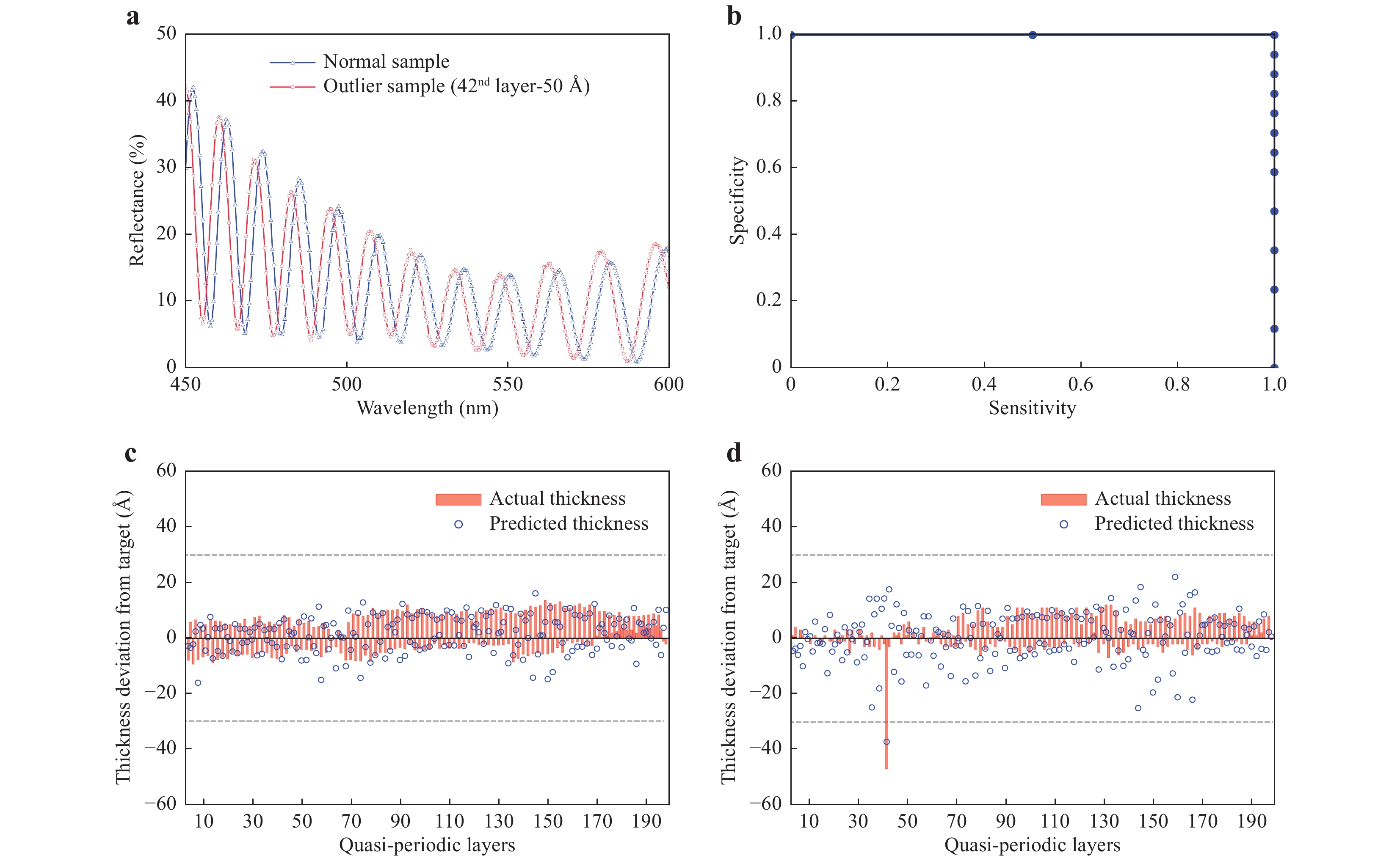
Fig. 5 Outlier detection results.
a Comparison of the measured reflectance between the normal condition (blue triangle line) sample and the outlier condition (red circle line) sample. b Sensitivity, the true positive rate, and specificity, the true negative rate, measure performance of outlier detection models. The plot in blue is drawn by modifying the outlier threshold from 10 Å to 50 Å. c Actual thickness (red bars) and predicted thickness (blue circles) deviations from the design target for one of the normal samples. d Actual thickness (red bars) and predicted thickness (blue circles) deviations from the design target for one of the outlier samples. The actual thickness deviation of the 42nd layer is −48 Å from the target, and the corresponding predicted thickness deviation is −37 Å from the target.When defining an outlier case with a one-layer thickness exceeding 30 Å from the target, all the normal samples were classified as normal cases, and all the outlier samples were classified as outlier cases. When we modified the outlier threshold from 10 Å to 50 Å, we obtained a sensitivity-specificity graph, as shown in Fig. 5b. For the normal samples, the thicknesses of all layers were predicted to have an average RMSE of 7.4 Å from the target (Fig. 5c). For the outlier samples, the average thickness of the 42nd layer was predicted to have a −35 Å deviation from the target. The remaining layers were predicted to have an average RMSE of 8.6 Å from the target (Fig. 5d). Therefore, machine learning based on simulated data could successfully detect the outliers (faulty devices) and the exact erroneous layer location in the device.
-
In summary, we demonstrated a non-destructive method to accurately characterise each layer thickness and to detect outliers in ultra-high-density 3D semiconductor devices consisting of more than 200 layers. The machine learning approach uses a data-driven algorithm that considers only the correlation between spectral data and thickness information. We could thus eliminate many measurement-related issues, such as absolute accuracy errors and drift in measurement instruments, as well as in situ material properties that are not completely measurable (e.g. changes in the wavelength-dependent refractive indices of each layer under different fabrication conditions). When using noisy data as input to machine learning algorithms, the trained model is robust against various measurement errors. In addition, our outlier detection method can detect significant thickness defects by using a relatively small number of TEM measurements (e.g. 18 samples used as normal cases in this work) and massive simulated data (used as outlier cases). As a result, this method is highly suitable for application in actual semiconductor manufacturing facilities. In our work, all the spectroscopic data were obtained in commercial 3D NAND manufacturing lines, and only tens to hundreds of TEM measurements were required for model training. It is noteworthy that the proposed approach is suitable for the thickness characterisation of multilayer systems composed of dielectric materials, whereas the thickness characterisation for multilayer systems composed of materials with high extinction coefficients, such as titanium nitride (TiN) or tungsten, is challenging owing to the relatively short penetration depth (of the order of tens of nanometres) of those materials.
Our demonstrated method can be readily applied for the total inspection of various 3D semiconductor devices as well as many other types of highly complex multilayer stacked devices, such as ultra-broadband dielectric mirrors for high field physics and ultrafast science36,37, thin-film bio-sensors for biotechnology38-40, and hyperbolic metamaterials41,42.
-
Theoretical model of spectroscopic data. In this section, we describe the process of deriving the theoretical values of reflectance, psi, and delta32. In a multilayer system, the tangential components of electric field
$ E $ and magnetic field$ H $ are continuous at the boundary between each layer. The tangential components of the electric field and the magnetic field at the interface of each layer have the following relationship:$$ \left[ {\begin{array}{*{20}{c}} {{E_t}}\\ {{H_t}} \end{array}} \right] = \left[ {\begin{array}{*{20}{c}} {\cos \delta }&{i\sin \delta /{\eta _1}}\\ {i{\eta _1}\sin \delta }&{\cos \delta } \end{array}} \right]\left[ {\begin{array}{*{20}{c}} {{E_b}}\\ {{H_b}} \end{array}} \right] $$ (1) where
$ {E}_{t} $ and$ {H}_{t} $ are the fields at the top interface;$ { E}_{b} $ and$ {H}_{b} $ are the fields at the bottom interface. The phase thickness$ \delta $ is expressed as$\dfrac{2\pi Nd \cos\theta }{\lambda }$ , where N is the complex refractive index of the layer; d denotes the layer thickness;$ \theta $ denotes the incident angle of the light;$ \lambda $ represents the light wavelength, and$ {\eta }_{1} $ is the optical admittance of the medium. In a multilayer system, Eq. 1 is extended for all layers and expressed by a matrix-cascaded system, as shown in Eq. 2:$$ \left[ {\begin{array}{*{20}{c}} B\\ C \end{array}} \right] = \left\{ {\mathop \prod \nolimits_{r = 1}^q \left[ {\begin{array}{*{20}{c}} {\cos {\delta _r}}&{i\sin {\delta _r}/{\eta _r}}\\ {i{\eta _r}\sin {\delta _r}}&{\cos {\delta _r}} \end{array}} \right]} \right\}\left[ {\begin{array}{*{20}{c}} 1\\ {{\eta _m}} \end{array}} \right] $$ (2) where
$ {\delta }_{r} $ is the phase thickness;$ {\eta }_{r} $ denotes the optical admittance of the r-th medium;$ {\eta }_{m} $ represents the optical admittance of the substrate; q is the number of layers, and B and C are the normalised electric and magnetic fields, respectively. Finally, we obtain the theoretical reflectance as follows:$$ R=r{r}^{*}=\left(\frac{{\eta }_{0}B-C}{{\eta }_{0}B+C}\right){\left(\frac{{\eta }_{0}B-C}{{\eta }_{0}B+C}\right)}^{*} $$ (3) where
$ r $ is the reflection coefficient, and$ {\eta }_{0} $ is the optical admittance of the incident medium. For an oblique incident angle,$ {\eta }_{r} $ is multiplied by$\dfrac{1}{{\cos}\theta }$ for p-polarisation and by$ {\cos}\theta $ for s-polarisation. Psi (Ψ) and delta (Δ) are derived from Eq. 4 as follows:$$ \frac{{r}_{p}}{{r}_{s}}={\tan}\left({\Psi }\right){e}^{i{\Delta }} $$ (4) where
$ {r}_{p} $ is the reflection coefficient for p-polarisation, and$ {r}_{s} $ is the reflection coefficient for s-polarisation. Varying the layer thickness leads to a change in the phase thickness for each wavelength of incident light, which results in changes in interference patterns of reflectance, psi, and delta.Data preparation. Semiconductor multilayer stacks that are used for commercial 3D NAND devices were obtained at different locations on each wafer. For multilayer thickness prediction, 148 normal samples were obtained from 10 different wafers (10 to 17 different locations on each wafer). A spectroscopic ellipsometer installed in the production lines was used to measure 991 psi-delta pairs for each sample. For outlier detection, 45 normal samples were obtained from four different wafers, and three outlier samples were obtained from one wafer. A total of 741 reflectances were measured for each sample using a spectroscopic reflectometer in the production lines. High-resolution cross-sectional images of the samples were obtained using TEM.
Noise injection method. Data augmentation is widely used for a relatively small amount of data in many applications43-45. Because our objective was to access only a small number of normal-condition samples (in commercial device production lines), we augmented the training samples by employing a noise-injection method. For multilayer metrology of normal conditions, 125 training samples were augmented by injecting noise, resulting in a total of 5,000 augmented data points (40 augmented data points per training sample). Note that 40 augmented data points for each training sample shared the same thickness profile. For each augmented data point, the spectral data could be shifted to the left or right (in wavelength) or shifted up or down as a whole from the original positions.
As shown in Fig. S4, α is added to all spectral data to inject vertical offset noise. To inject lateral offset noise by β, shifted spectral data at (216 + β) nm to (905 + β) nm should be obtained. However, since psi and delta were measured for wavelengths of 216–905 nm, we interpolated the original spectral data into shifted spectral ranges to obtain the shifted spectral data. When shifting spectral data to the left or right, redundant values can be generated because the shifted spectral data deviate from the actual measured range. These redundant values are truncated at both ends. A total of 12 redundant values were removed. Thus, 1,970 dimensional inputs were used.
Considering various possible noise sources during measurement (such as drift errors, wavelength errors, and refractive index changes), we added different amounts of noise under various conditions to the original spectral data. As shown in Fig. S5, injection of vertical offset noise uniformly distributed from −0.04 to +0.04 and lateral offset noise uniformly distributed from −6 to +6 nm was the best condition for thickness prediction performance for the validation set. For an outlier detection test, we also augmented the training samples by employing the noise injection method. Eighteen training samples representing normal conditions were increased to 1,800 augmented data points (100 augmented data per training sample). For lateral noise injection, three redundant values were truncated at each end such that the shifted reflectance did not contain the redundant values. A total of 735 dimensional inputs were used. As shown in Fig. S5, injection of lateral offset noise uniformly distributed from −4 to +4 nm without using vertical noise injection was the best condition for thickness prediction performance for the validation set.
Performance comparison with psi and delta combinations. For multilayer metrology under normal conditions, we compared the RMSE of the validation set using a linear model to determine which combination of spectral data (psi and delta) should be used as the input to the model. As shown in Table S2, when both psi and delta are used, the RMSE of the validation set has the lowest value of 2.75 Å. Because machine learning learns the correlation between the input (spectroscopic measurements) and the output (layer thicknesses) rather than interpreting the physical meaning of the input data, there is no significant difference in the prediction RMSE, regardless of whether psi or delta is used. From these results, we find that the thickness prediction model performs best when using all spectroscopic data as inputs.
Evaluation of machine learning models For multilayer metrology under normal conditions, we first randomly split 148 samples into 125 training samples and 23 test samples. The 125 training samples were divided into five folds (25 samples per fold). One hundred samples (four of five folds) were converted to 4,000 augmented data using the noise injection method to train the model, and the remaining 25 samples (one of five folds) were used as the validation set to evaluate the model. Each fold was used as a validation set, and five validation results were averaged to measure the model performance. This method, called K-fold cross-validation46,47 (in this case, five-fold cross-validation), is widely used to identify the best model. For the model evaluation, the RMSE between the predicted thicknesses and the actual thicknesses of the validation set was used. As shown in Table S3, the RMSE of the validation set was found to be the lowest for the linear model. We evaluated the performance of the linear model according to the training data size, which is shown as the learning curve in Fig. S6. The RMSE was calculated by increasing the training data size from 40 to 4,000 (with 40 intervals).
As the number of training data increased, the RMSE of the training set increased because it became more difficult to perfectly fit the training data. Meanwhile, the RMSE of the validation set decreased as the model became better fitted to unseen data. Because the RMSE of the validation set approached the RMSE of the training set until settling, the 4,000 training data were sufficient to train the linear model without overfitting.
For the implementation, we used a Titan X graphical processing unit (GPU). Generating 5,000 augmented data from 125 training samples by the noise-injection method required approximately 2 s. The complete training for the linear model required approximately 116 s. With the trained model, the prediction time for the test samples was less than 0.01 s. The most time-consuming process in this study was the model validation process because all the models were evaluated with the five-fold cross-validation technique. The linear model, support vector regression (SVR48), and deep neural network (DNN) required ~550 s, ~9 h, and ~2 h for the cross-validation, respectively. Furthermore, to evaluate the model by modifying the hyperparameters (such as the number of hidden neurons or level of regularisation), the validation time for each model was multiplied by the number of hyperparameter sets used. However, since we found that the linear model performed the best in this study, the actual model validation time was relatively short.
Implementation details of machine learning models. For multilayer metrology under normal conditions, we used three different machine learning models: SVR, linear regression46, and an artificial neural network (ANN49,50). All these models are regression models that predict continuous values (layer thicknesses). For all spectral data, feature standardisation is applied; thus, each feature vector has zero mean and unit variance. We compared the RMSE of the validation set with various conditions for each model. As shown in Fig. S7, when using the DNN model with a large number of hidden neurons, the RMSE of the training set converges to zero; however, the RMSE of the validation set does not decrease on account of overfitting during training. For the linear model, we applied L2 regularisation46 to avoid overfitting and used a conjugate gradient function51 with 1,000 iterations to minimise cost function J as follows:
$$ J = \frac{1}{{2N}}\left[ {\mathop \sum \nolimits_{i = 1}^N {{\left( {{p_i} - {y_i}} \right)}^2} + \lambda {{\left\| {\bf{w}} \right\|}^2}} \right] $$ (5) where N is the number of training samples;
$ {p}_{i} $ denotes the predicted thickness;$ {y}_{i} $ is the actual thickness;$ \lambda $ represents a parameter that controls the level of L2 regularisation, and w is the weight vector. A step-by-step algorithm operation process for the linear model is provided as a flow chart shown in Fig. S9. For the SVR model, we used a radial basis function as the kernel function. Scikit-learn52 was used for implementing the SVR with cost function J as follows:$$ J = C\mathop \sum \nolimits_{i = 1}^N {L_\varepsilon }\left( {{p_i} - {y_i}} \right) + \frac{1}{2}{\left\| {\bf{w}} \right\|^2} $$ (6) where
$ C $ is a regularisation parameter.$ {L}_{\varepsilon } $ is an ε-insensitive loss function given by$${L_\varepsilon }\left( {{p_i} - {y_i}} \right) = \left\{ \begin{aligned} & {0,\;\qquad\quad\ \ if\left| {{p_i} - {y_i}} \right| < \varepsilon ;}\\ & {\left| {{p_i} - {y_i}} \right| - \varepsilon ,\;{\rm{otherwise}}} \end{aligned}\right.$$ (7) Here, ε is the margin of tolerance, where no penalty is given to errors. ANNs with different architectures were implemented using Tensorflow53. For the ANN models, batch normalisation54, a ReLU activation function55, and dropout56 were applied. Batch normalisation and ReLU were applied to all hidden layers, while dropout was applied to the last hidden layer. A linear activation function was used for the output layer. As the best result for each ANN model, for the two-layer neural network (NN), eight neurons were used for the hidden layer without a dropout layer. For the three-layer DNN, 512 neurons were used for each hidden layer with a dropout layer (50% drop probability). For the four-layer DNN, 512 neurons were used for each hidden layer with a dropout layer (50% drop probability). The batch size was 128 in all cases. We used the Adam optimiser57 with 10,000 epochs. It should be noted that an epoch denotes one full training iteration for each training data. The learning rate was 0.003.
Outlier detection methods To detect outliers, we used simulated spectroscopic data for model training. The matrix method32 was used to obtain the theoretical values of reflectance (see the ‘Theoretical model of spectroscopic data’ section in ‘Methods’). To simulate the spectroscopic data, the thickness of each layer and the refractive index of each medium were required. We used the measured refractive index obtained by a single layer measurement of each material with an ellipsometer (Fig. S8) as the refractive index of each material (oxide, nitride, and Si substrate) in the modelling. Because the outlier detection method focuses on detecting relatively large thickness changes, precise optical modelling by accurate refractive index characterisation was not required. We assumed that all the oxide and nitride layers shared the same oxide and nitride refractive indices, respectively. In addition, we assumed that there were no surface roughness or interface layers in the multilayer structures, which was also confirmed by the TEM measurement results.
Instead of using one model to predict the thickness of all layers, multiple models (i.e. one model per layer) were used to predict the multilayer thickness. The reasons were (a) to avoid overfitting the model to a large amount of simulated data generated for potential outlier cases, and (b) to magnify the sensitivity to the critical thickness changes of a single layer.
To train and test the outlier detection models, we prepared 45 normal samples and 3 outlier samples. As shown in Fig. S3, the 45 normal samples were first randomly split into 18 training, 10 validation, and 17 test samples. The three outlier samples were randomly split into one validation and two test samples. Eighteen normal samples were increased to 1,800 augmented data by the noise injection method, and 1,000 simulated data, which were designed with a relatively large thickness variation in each layer, were generated. When designing the simulated outlier case data, the thickness of the outlier layer was uniformly distributed within a ±20% variation with respect to the reference thickness, and the thicknesses of the other layers were uniformly distributed within ±4% of the reference thickness. Here, the reference thickness denotes the average thickness of each layer for the 18 normal samples used for model training. A total of 2,800 training data (1,800 for normal cases and 1,000 for outlier cases) were used to train each outlier detection model. We used the linear model (with the L2 regularisation parameter of 100) for the outlier detection model because we found that the linear model performed the best in thickness characterisation of the multilayer (Fig. S7).
To determine the best noise-injection condition for the 18 training samples, 10 normal samples and one outlier sample were used as the validation set. We found that the lowest RMSE of the validation set was 4.78 Å when applying lateral offset noise uniformly distributed from −4 to +4 nm without vertical noise injection. For model testing, 17 normal samples and 2 outlier samples were put into each model to predict the thickness of each layer. Although a sample with a single-layer defect is used in this study, we anticipated that defects in multiple layers could be detected because our scheme is based on multiple models (i.e. one model per layer) for outlier detection.
-
This research was supported by the Industry–Academia Cooperation Program of Samsung Electronics Co., Ltd.
Non-destructive thickness characterisation of 3D multilayer semiconductor devices using optical spectral measurements and machine learning
- Light: Advanced Manufacturing 2, Article number: 1 (2021)
- Received: 26 July 2020
- Revised: 23 October 2020
- Accepted: 06 November 2020 Published online: 12 January 2021
doi: https://doi.org/10.37188/lam.2021.001
Abstract: Three-dimensional (3D) semiconductor devices can address the limitations of traditional two-dimensional (2D) devices by expanding the integration space in the vertical direction. A 3D NOT-AND (NAND) flash memory device is presently the most commercially successful 3D semiconductor device. It vertically stacks more than 100 semiconductor material layers to provide more storage capacity and better energy efficiency than 2D NAND flash memory devices. In the manufacturing of 3D NAND, accurate characterisation of layer-by-layer thickness is critical to prevent the production of defective devices due to non-uniformly deposited layers. To date, electron microscopes have been used in production facilities to characterise multilayer semiconductor devices by imaging cross-sections of samples. However, this approach is not suitable for total inspection because of the wafer-cutting procedure. Here, we propose a non-destructive method for thickness characterisation of multilayer semiconductor devices using optical spectral measurements and machine learning. For > 200-layer oxide/nitride multilayer stacks, we show that each layer thickness can be non-destructively determined with an average of approximately 1.6 Å root-mean-square error. We also develop outlier detection models that can correctly classify normal and outlier devices. This is an important step towards the total inspection of ultra-high-density 3D NAND flash memory devices. It is expected to have a significant impact on the manufacturing of various multilayer and 3D devices.
Research Summary
Multilayer metrology: Combining optical spectral measurements and machine learning
With recent explosive demand for data storage, ranging from data centres to smart devices, the need for higher-capacity and more compact memory devices is constantly increasing. The 3D-NAND flash memory is the most commercially successful 3D memory device today, and its demand is growing exponentially. As each layer thickness corresponds to the effective channel length in such devices, accurate characterisation and control of layer-by-layer thickness is critical. By combining optical spectral measurements and machine learning, Jungwon Kim from Korea Advanced Institute of Science and Technology and colleagues demonstrate a non-destructive method for thickness characterisation of each layer in 3D multilayer semiconductor devices. The team could characterise the thickness of each layer with an average root-mean-square error of only 1.6 Å over more than 200 layers structure.


Rights and permissions
Open Access This article is licensed under a Creative Commons Attribution 4.0 International License, which permits use, sharing, adaptation, distribution and reproduction in any medium or format, as long as you give appropriate credit to the original author(s) and the source, provide a link to the Creative Commons license, and indicate if changes were made. The images or other third party material in this article are included in the article′s Creative Commons license, unless indicated otherwise in a credit line to the material. If material is not included in the article′s Creative Commons license and your intended use is not permitted by statutory regulation or exceeds the permitted use, you will need to obtain permission directly from the copyright holder. To view a copy of this license, visit http://creativecommons.org/licenses/by/4.0/.

 DownLoad: