
Collection | 30 May 2023
Photonic integration and optoelectronics convergence
Integrated photonics consists of integrating multiple photonic devices/functions on a single Photonic Integrated Chip (PIC), while optoelectronics convergence is building the bridge between photonics and microelectronics. Empowered by various nanofabrication techniques on diverse innovative material platforms, remarkable advances have been made in photonic integration and optoelectronics convergence in the last decade. Those exciting progresses took place in the areas of materials, processing techniques, innovations on both passive and active devices, chip architectures, levels of integration complexity and density, and beyond. Integration offers size and cost reduction, faster processing speed, larger information capacity, higher energy efficiency, more versatility, and consequently broader impact to the human society. Various miniaturized devices are made available enabling better existing applications, new emerging applications, and opening new market opportunities in communications, biomedicine, sensing, computing, automotive and metrology, etc.
This special issue aims at capturing the most exciting advances in the leading edge of photonic integration and optoelectronics convergence, including new material platforms, new fabrication and characterization technologies, new device physics and architectures, new design principle for miniaturized components, micro- and nano-photonics devices, the rising and potential applications. We hope to provide an overview as well as insightful perspectives of the field by collecting contributions from leading experts and major industry players to promote the breakthrough science and impactful applications in photonic integration and optoelectronics convergence.
This issue is co-edited by
Prof. Lianshan Yan, Dean, School of Information Science and Technology, Southwest Jiaotong University, China
Prof. Baohua Jia, Director, Centre for Atomaterials Sciences and Technologies, RMIT University, Australia
Dr. Di Liang, Director, Alibaba Cloud, Alibaba Group, USA
Prof. David Moss, Director, Optical Science Centre, Swinburne University of Technology, Australia
Dr. Xi Xiao, CEO, National Information Optoelectronics Innovation Center, China
-
Article
Dual-point noncoaxial rotational Doppler effect towards synthetic OAM light fields for real-time rotating axis detection
 Published , Published online: 26 September 2023 , doi: 10.37188/lam.2023.027
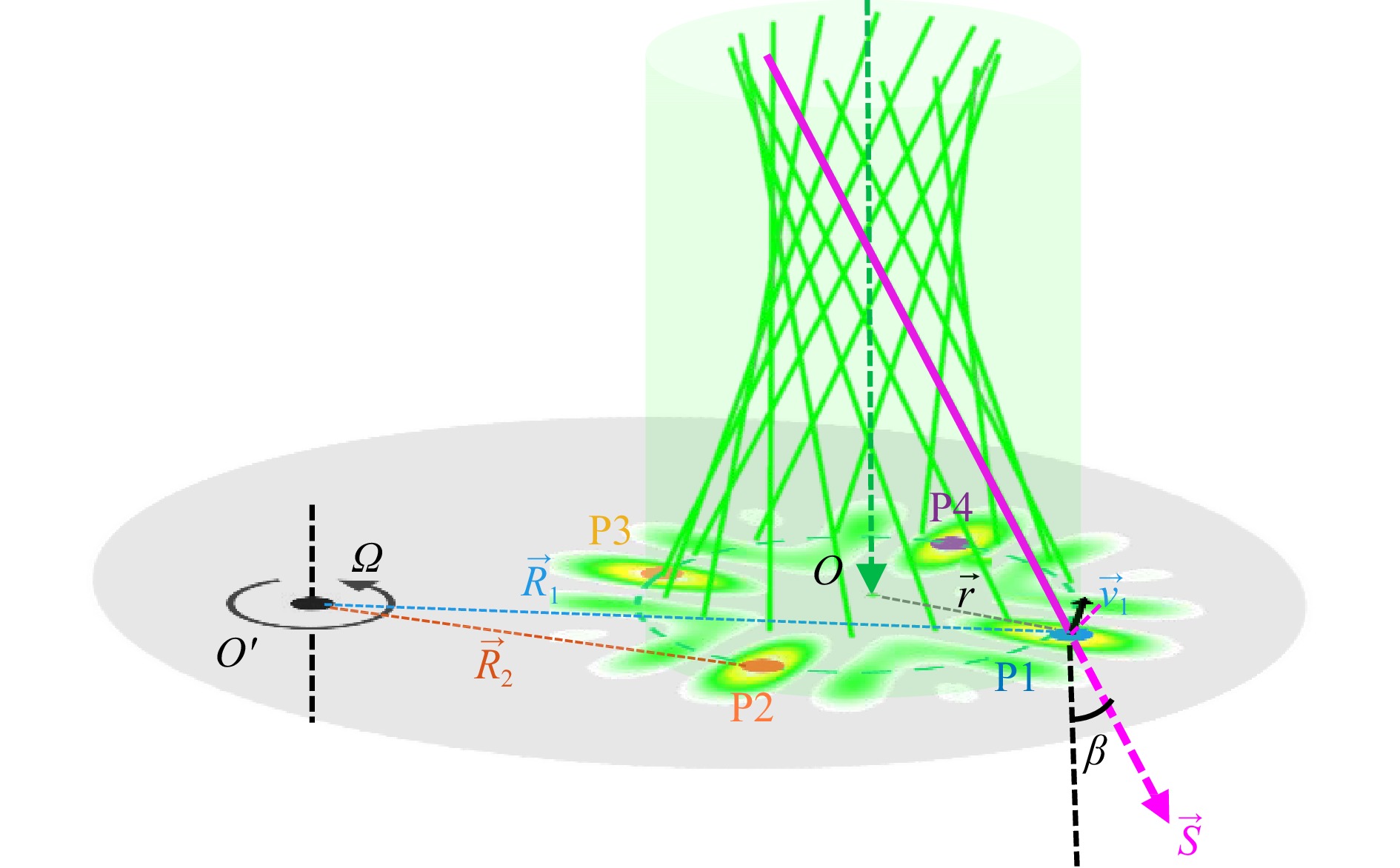
Probing the axis of a rotator is important in astrophysics, aerospace, manufacturing, machinery, automation, and virtual reality, etc. Existing optical solutions commonly require multiple sequential measurements via symmetry-broken light fields, which make them time-consuming, inefficient, and prone to accumulated errors. Herein, we propose the concept of a dual-point noncoaxial rotational Doppler effect (DNRDE) and demonstrate a one-shot detection technique to solve this problem. An on-demand synthetic orbital angular momentum (OAM) light beam impinges on a rotating scatterer surface, supporting dual-point rotational Doppler shifts, in which the information of the rotating axis is acquired by comparing these two frequency shifts with a prescribed threshold. The existence of arbitrary dual-point Doppler shifts enables the one-time direct identification of rotating axis orientations, which is fundamentally inaccessible in single-point detection. This robust detection technique is compatible with generalised synthetic OAM light fields by utilising optical modal filters. Compared with traditional approaches, our DNRDE-driven detection approach exhibits a four-fold enhancement in measurement speed, higher energy efficiency, and superior accuracy with a maximal absolute measurement error of 2.23°. The proposed dual-point detection method holds great promise for detecting rotating bodies in various applications, such as astronomical surveys and industrial manufacturing.
-
Article
Facile integration of electro-optic SiO2/ITO heterointerfaces in MIS structures for CMOS-compatible plasmonic waveguide modulation
 Published , Published online: 22 December 2023 , doi: 10.37188/lam.2023.038
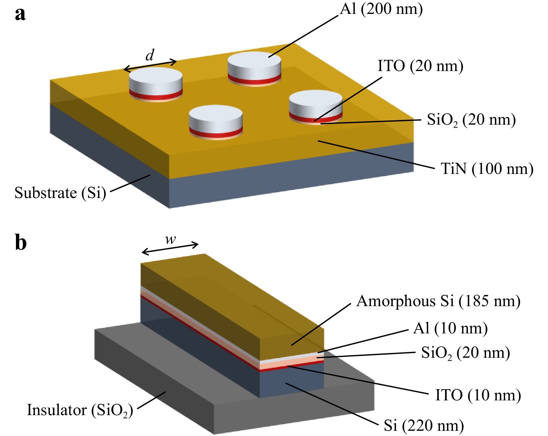
By taking advantage of the absence of diffraction limit restrictions in plasmonic structures, strong modal confinement is made possible, paving the way for improved optical processes and miniaturized photonic circuit integration. Indium tin oxide (ITO) has emerged as a promising plasmonic material that serves as a relatively low-carrier density Drude metal by its electro-optic tunability and versatility as an integrative oxide. We herein demonstrate the facile integration of SiO2/ITO heterointerfaces into metal–insulator–semiconductor (MIS) electro-optic structures. The first MIS device employs a SiO2/ITO heterostructure grown on thin polycrystalline titanium nitride (poly-TiN) and capped at the ITO side with thin aluminum (Al) film contact electrode. The TiN interlayer acts as a bottom electrode, forming a metal–insulator–semiconductor-metal (MISM) heterojunction device, and grows directly on (100)-oriented silicon (Si). This MISM device enables one to examine the electrical properties of semiconductive ITO layers. The second MIS device incorporates a semiconductive ITO layer with a SiO2 dielectric spacer implemented on a silicon-on-insulator (SOI) platform, forming a graded-index coupled hybrid plasmonic waveguide (CHPW) modulator. This device architecture represents a crucial step towards realizing plasmonic modulation using oxide materials. The CHPW device performance presented herein provides a proof-of-concept that demonstrates the advantages offered by such device topology to perform optical modulation via charge carrier dispersion. The graded-index CHPW can be dynamically reconfigured for amplitude, phase, or 4-quadrature amplitude modulation utilizing a triode-like biasing strategy. It exhibited extinction ratio (ER) and insertion loss (IL) levels of around 1 dB/μm and 0.128 dB/μm, respectively, for a 10 μm waveguide length.
-
Article
Integrated optical parametric amplifiers in silicon nitride waveguides incorporated with 2D graphene oxide films
 Published , Published online: 29 December 2023 , doi: 10.37188/lam.2023.039
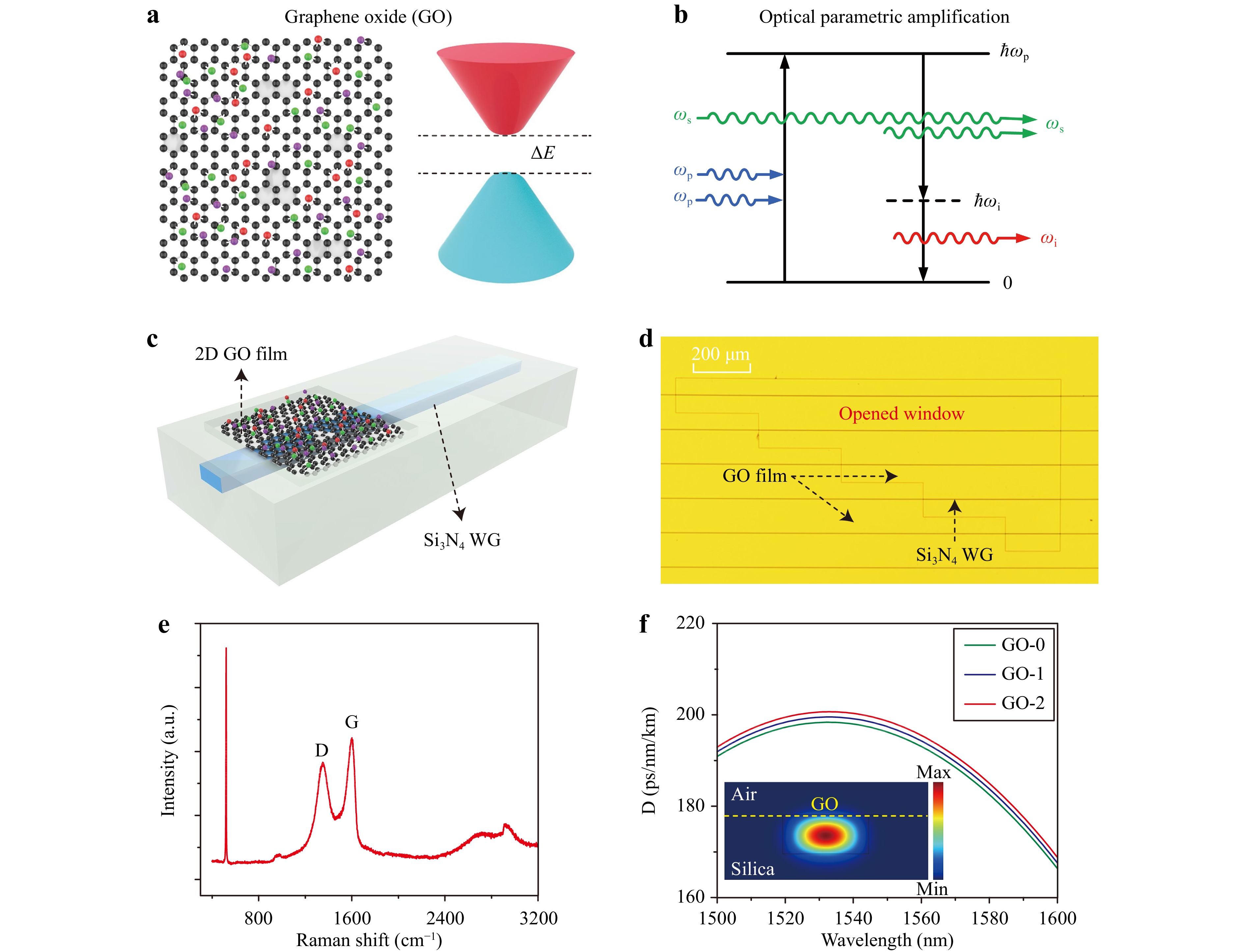
Optical parametric amplification (OPA) represents a powerful solution to achieve broadband amplification in wavelength ranges beyond the scope of conventional gain media, for generating high-power optical pulses, optical microcombs, entangled photon pairs and a wide range of other applications. Here, we demonstrate optical parametric amplifiers based on silicon nitride (Si3N4) waveguides integrated with two-dimensional (2D) layered graphene oxide (GO) films. We achieve precise control over the thickness, length, and position of the GO films using a transfer-free, layer-by-layer coating method combined with accurate window opening in the chip cladding using photolithography. Detailed OPA measurements with a pulsed pump for the fabricated devices with different GO film thicknesses and lengths show a maximum parametric gain of ~24.0 dB, representing a ~12.2 dB improvement relative to the device without GO. We perform a theoretical analysis of the device performance, achieving good agreement with experiment and showing that there is substantial room for further improvement. This work represents the first demonstration of integrating 2D materials on chips to enhance the OPA performance, providing a new way of achieving high performance photonic integrated OPA by incorporating 2D materials.
-
Review
Two-photon lithography for integrated photonic packaging
 Published , Published online: 01 November 2023 , doi: 10.37188/lam.2023.032
Photonic integrated circuits (PICs) have long been considered as disruptive platforms that revolutionize optics. Building on the mature industrial foundry infrastructure for electronic integrated circuit fabrication, the manufacturing of PICs has made remarkable progress. However, the packaging of PICs has often become a major barrier impeding their scalable deployment owing to their tight optical alignment tolerance, and hence, the requirement for specialty packaging instruments. Two-photon lithography (TPL), a laser direct-write three-dimensional (3-D) patterning technique with deep subwavelength resolution, has emerged as a promising solution for integrated photonics packaging. This study provides an overview of the technology, emphasizing the latest advances in TPL-enabled packaging schemes and their prospects for adoption in the mainstream photonic industry.
-
Review
Hybrid-integrated chalcogenide photonics
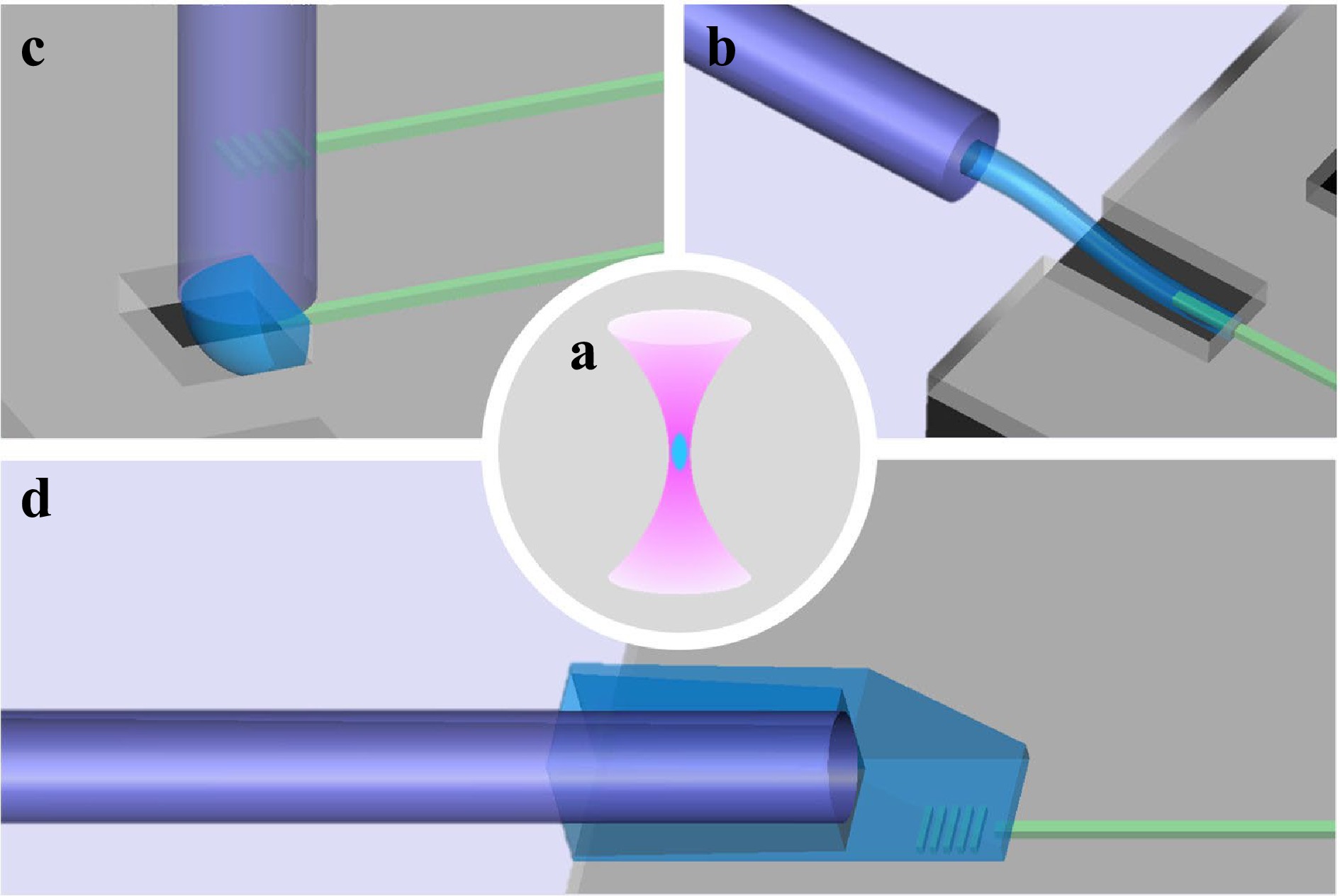
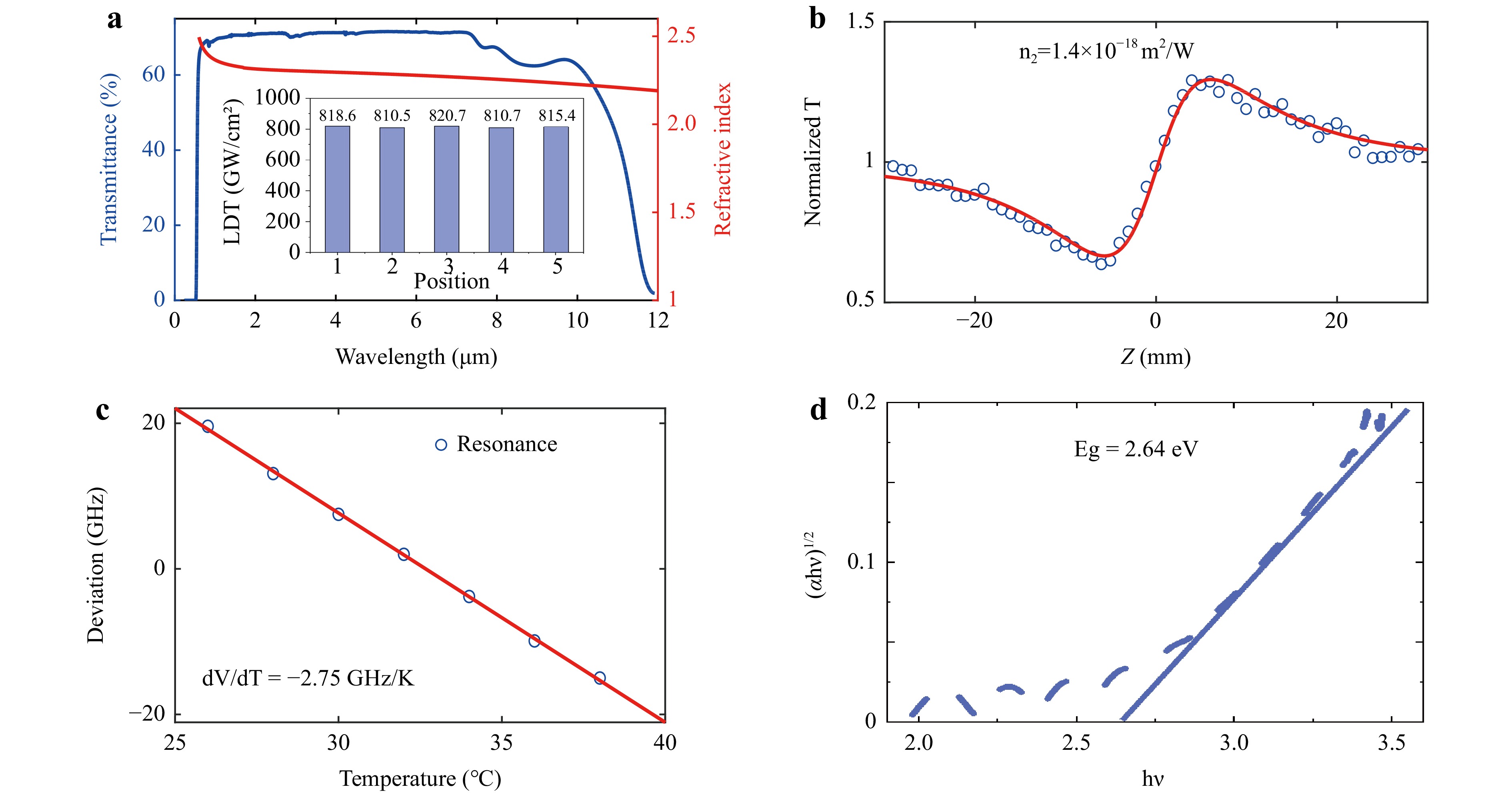 Published , Published online: 22 September 2023 , doi: 10.37188/lam.2023.024
High-quality photonic materials are critical for promoting integrated photonic devices with broad bandwidths, high efficiencies, and flexibilities for high-volume chip-scale fabrication. Recently, we designed a home-developed chalcogenide glass (ChG)-Ge25Sb10S65 (GeSbS) for optical information processing chips and systems, which featured an ultrabroad transmission window, a high Kerr nonlinearity and photoelastic coefficient, and compatibility with the photonic hybrid integration technology of silicon photonics. Chip-integrated GeSbS microresonators and microresonator arrays with high quality factors and lithographically controlled fine structures were fabricated using a modified nanofabrication process. Moreover, considering the high Kerr nonlinearity and photoelastic effect of ChGs, we realised a novel ChG hybrid integrated chip, inspired by recent advances in integrated soliton microcombs and acousto-optic (AO) modulators.
-
Review
Recent progress on micro-LEDs
 Published , Published online: 06 December 2023 , doi: 10.37188/lam.2023.031
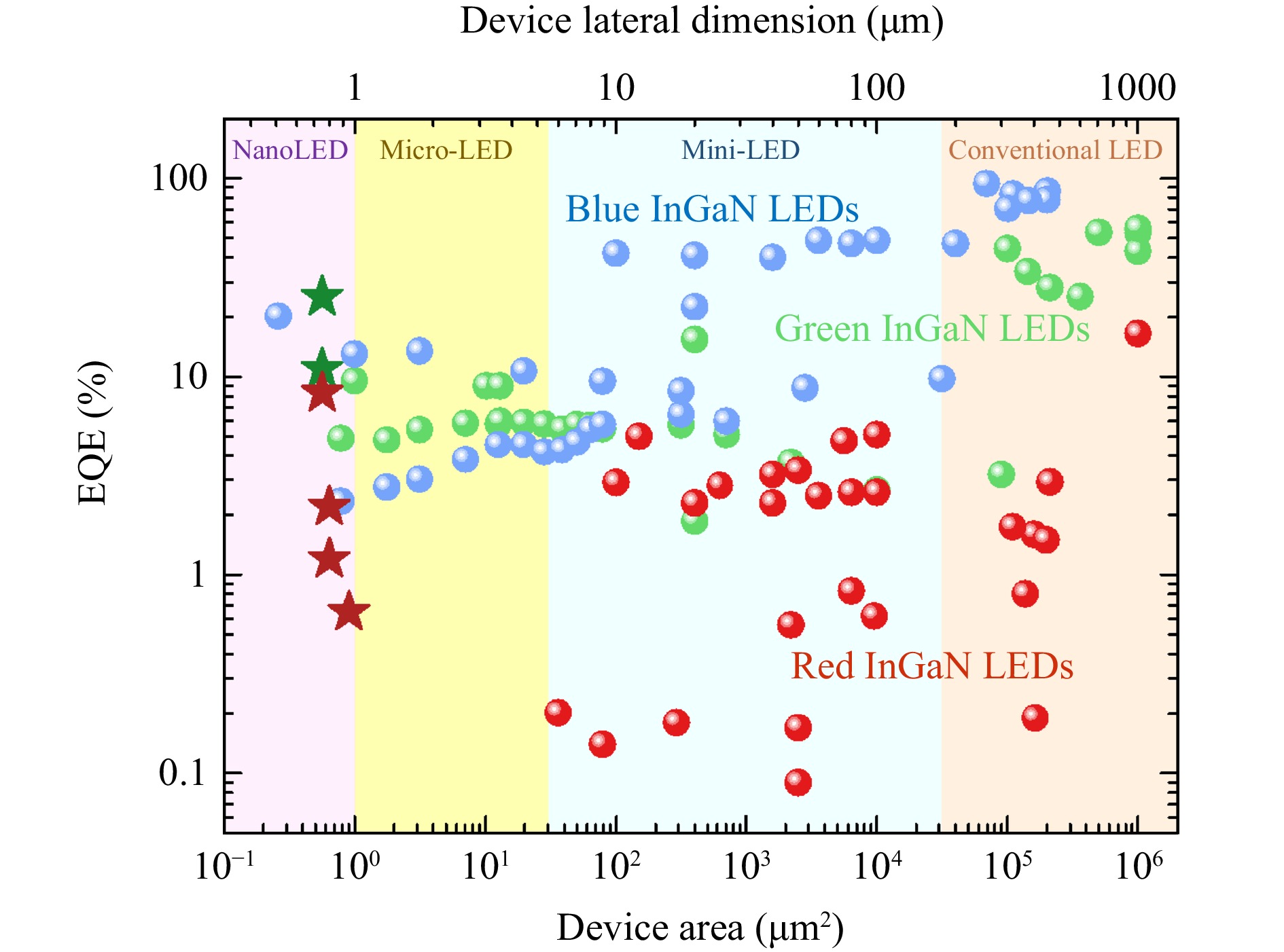
With the advent of technologies such as augmented/virtual reality (AR/VR) that are moving towards displays with high efficiency, small size, and ultrahigh resolution, the development of optoelectronic devices with scales on the order of a few microns or even smaller has attracted considerable interest. In this review article we provide an overview of some of the recent developments of visible micron-scale light emitting diodes (LEDs). The major challenges of higher surface recombination for smaller size devices, the difficulty in attaining longer emission wavelengths, and the complexity of integrating individual, full color devices into a display are discussed, along with techniques developed to address them. We then present recent work on bottom-up nanostructure-based sub-micron LEDs, highlighting their unique advantages, recent developments, and promising potential. Finally, we present perspectives for future development of micro-LEDs for higher efficiencies, better color output and more efficient integration.
-
Article
Large viewing angle holographic 3D display system based on maximum diffraction modulation
 Published , Published online: 20 July 2023 , doi: 10.37188/lam.2023.018
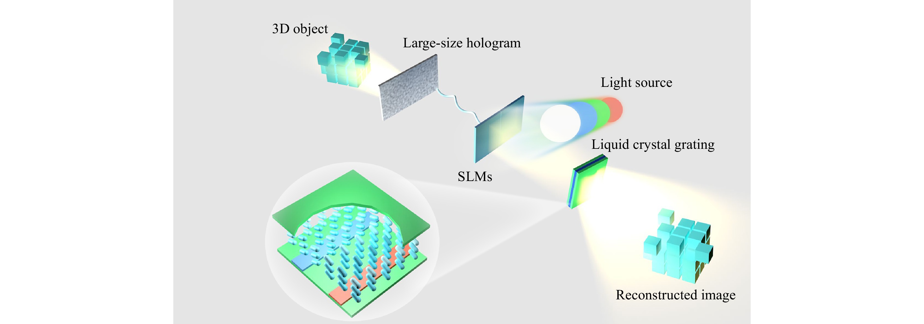
An ideal holographic 3D display should have the characteristics of large viewing angle, full color, and low speckle noise. However, the viewing angle of the holographic 3D display is usually limited by existing strategies, which vastly hinders its extensive application. In this paper, a large viewing angle holographic 3D display system based on maximum diffraction modulation is proposed. The core of the proposed system comprises the spatial light modulators (SLMs) and liquid crystal grating. We also present a new feasible scheme for the realization of large viewing angle holographic 3D display. This is achieved by considering the maximum diffraction angle of SLM as the limited diffraction modulation range of each image point. By doing so, we could not only give access to the maximum hologram size of the object, but also tune the reconstructed image of secondary diffraction by using a self-engineered liquid crystal grating. More importantly, the proposed maximum diffraction modulation scheme enables the viewing angle of the proposed system to be enlarged to 73.4°. The proposed system has huge application potential in the fields such as education, culture, and entertainment.
-
Article
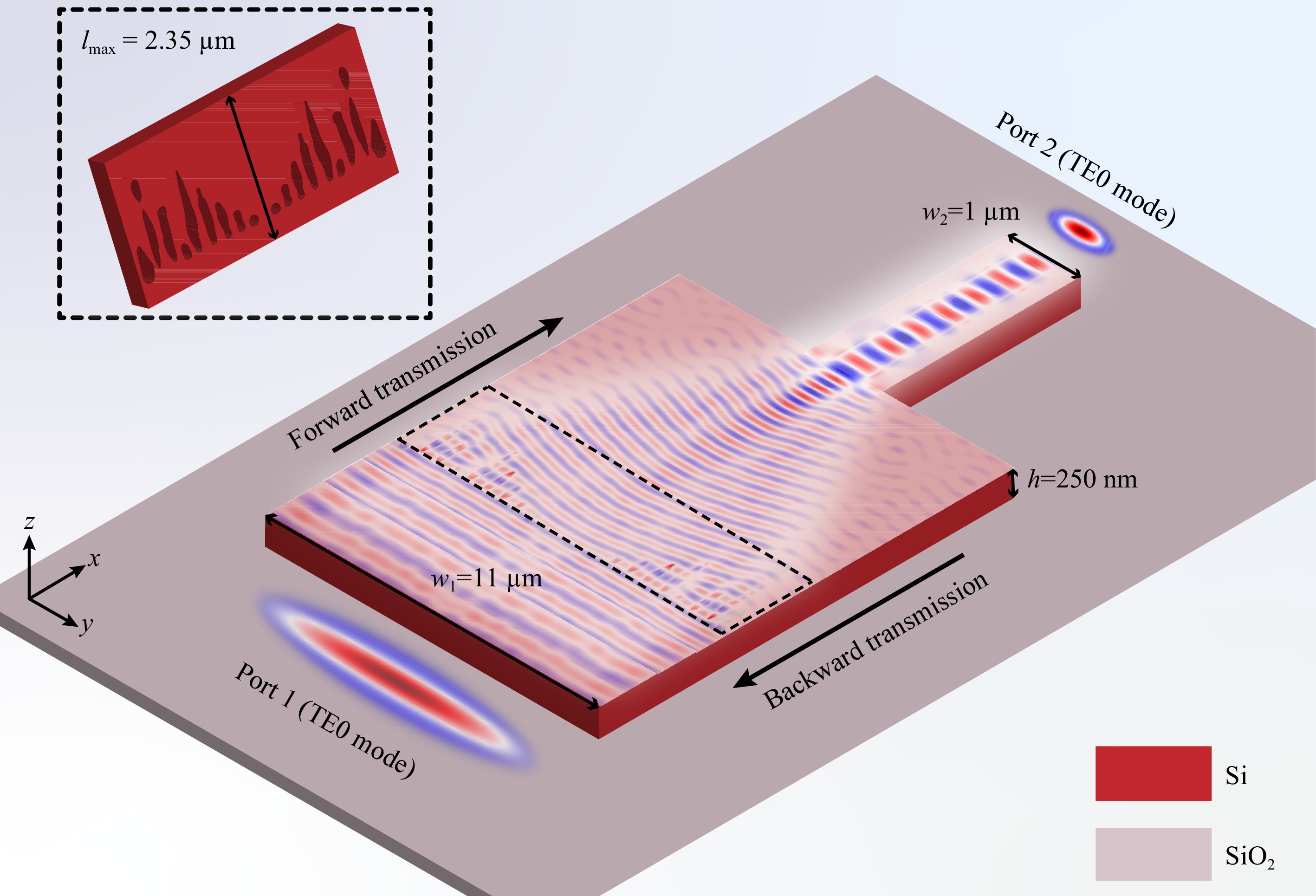
High-fidelity mode scaling via topological-optimized on-chip metalens for compact photonic interconnection
 Published , Published online: 18 August 2023 , doi: 10.37188/lam.2023.020
Photonic integrated circuits (PICs) have attracted significant interest in communication, computation, and biomedical applications. However, most rely on highly integrated PICs devices, which require a low-loss and high-integration guided wave path. Owing to the various dimensions of different integrated photonic devices, their interconnections typically require waveguide tapers. Although a waveguide taper can overcome the width mismatch of different devices, its inherent tapering width typically results in a long length, which fundamentally limits the efficient interconnection between devices with a high scaling ratio over a short distance. Herein, we proposed a highly integrated on-chip metalens that enables optical interconnections between devices with high width-scaling ratios by embedding a free-form metasurface in a silicon-on-insulator film. The special geometric features endow the designed metalens with high coupling efficiency and high integration. The device has a footprint of only 2.35 μm in the longitudinal direction and numerical aperture of 2.03, enabling beam focusing and collimation of less than 10 μm between devices with width-scaling ratio of 11. For the fundamental transverse electric field (TE0) mode, the relative transmittance is as high as 96% for forward incidence (from wide to narrow waveguides), whereas the metalens can realize wavefront shaping for backward incidence, which can be used in optical phase arrays. This study provides new ideas for optical interconnect design and wavefront shaping in high-integration PICs. Our design approach has potential applications in directional radiators, LiDAR, on-chip optical information processing, analogue computing, and imaging.
-
Article
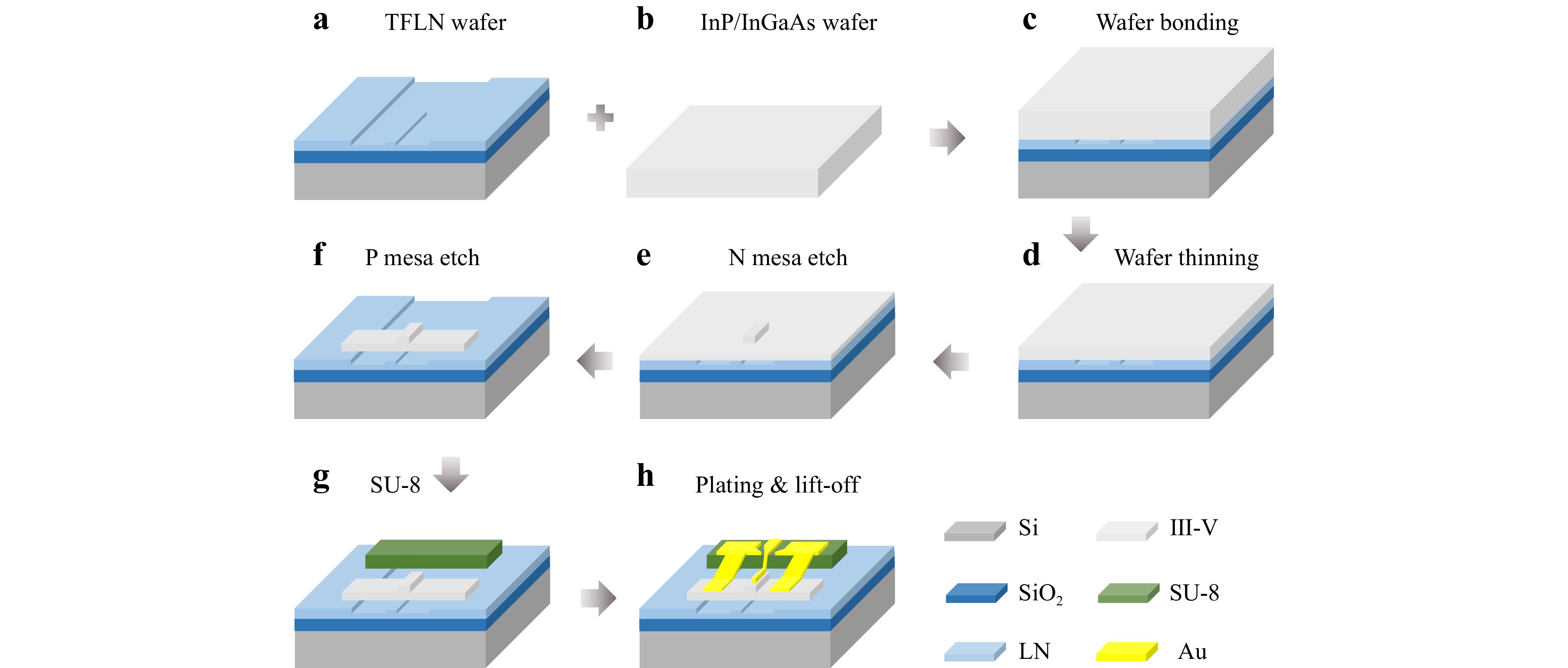
Ultra-wideband Waveguide-coupled Photodiodes Heterogeneously Integrated on a Thin-film Lithium Niobate Platform
 Published , Published online: 12 September 2023 , doi: 10.37188/lam.2023.030
With the advantages of large electro-optical coefficient, wide transparency window, and strong optical confinement, thin-film lithium niobate (TFLN) technique has enabled the development of various high-performance optoelectronics devices, ranging from the ultra-wideband electro-optic modulators to the high-efficient quantum sources. However, the TFLN platform does not natively promise lasers and photodiodes. This study presents an InP/InGaAs modified uni-traveling carrier (MUTC) photodiodes heterogeneously integrated on the TFLN platform with a record-high 3-dB bandwidth of 110 GHz and a responsivity of 0.4 A/W at a 1,550-nm wavelength. It is implemented in a wafer-level TFLN-InP heterogeneous integration platform and is suitable for the large-scale, multi-function, and high-performance TFLN photonic integrated circuits.
-
Review
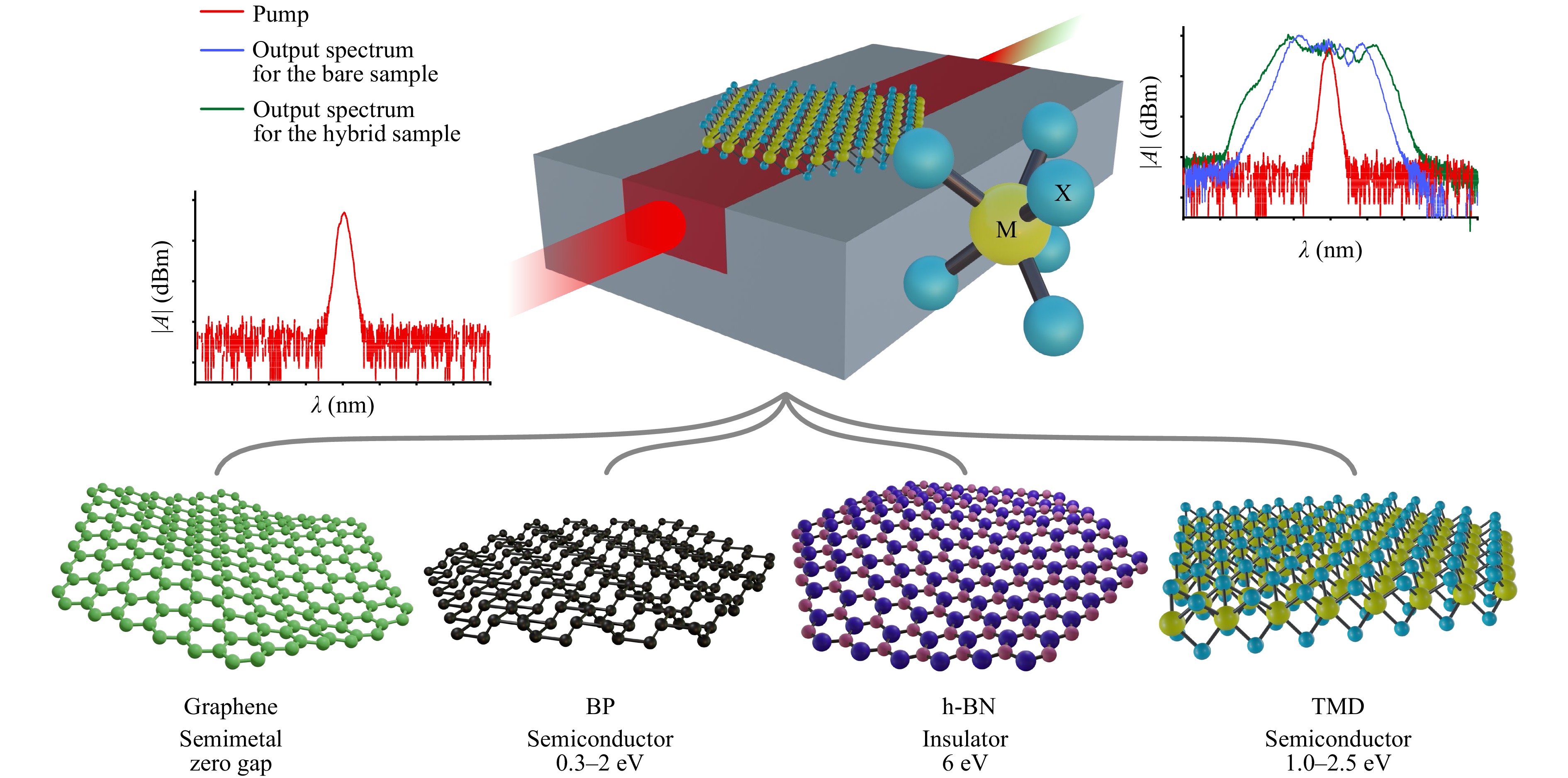
Hybrid integration of 2D materials for on-chip nonlinear photonics
 Published , Published online: 01 August 2023 , doi: 10.37188/lam.2023.014
Interests surrounding the development of on-chip nonlinear optical devices have been consistently growing in the past decades due to the tremendous applications, such as quantum photonics, all-optical communications, optical computing, on-chip metrology, and sensing. Developing efficient on-chip nonlinear optical devices to meet the requirements of those applications brings the need for new directions to improve the existing photonic approaches. Recent research has directed the field of on-chip nonlinear optics toward the hybrid integration of two-dimensional layered materials (such as graphene, transition metal dichalcogenides, and black phosphorous) with various integrated platforms. The combination of well-known photonic chip design platforms (e.g., silicon, silicon nitride) and different two-dimensional layered materials has opened the road for more versatile and efficient structures and devices, which has the great potential to unlock numerous new possibilities. This review discusses the modeling and characterization of different hybrid photonic integration structures with two-dimensional materials, highlights the current state of the art examples, and presents an outlook for future prospects.
-
Article
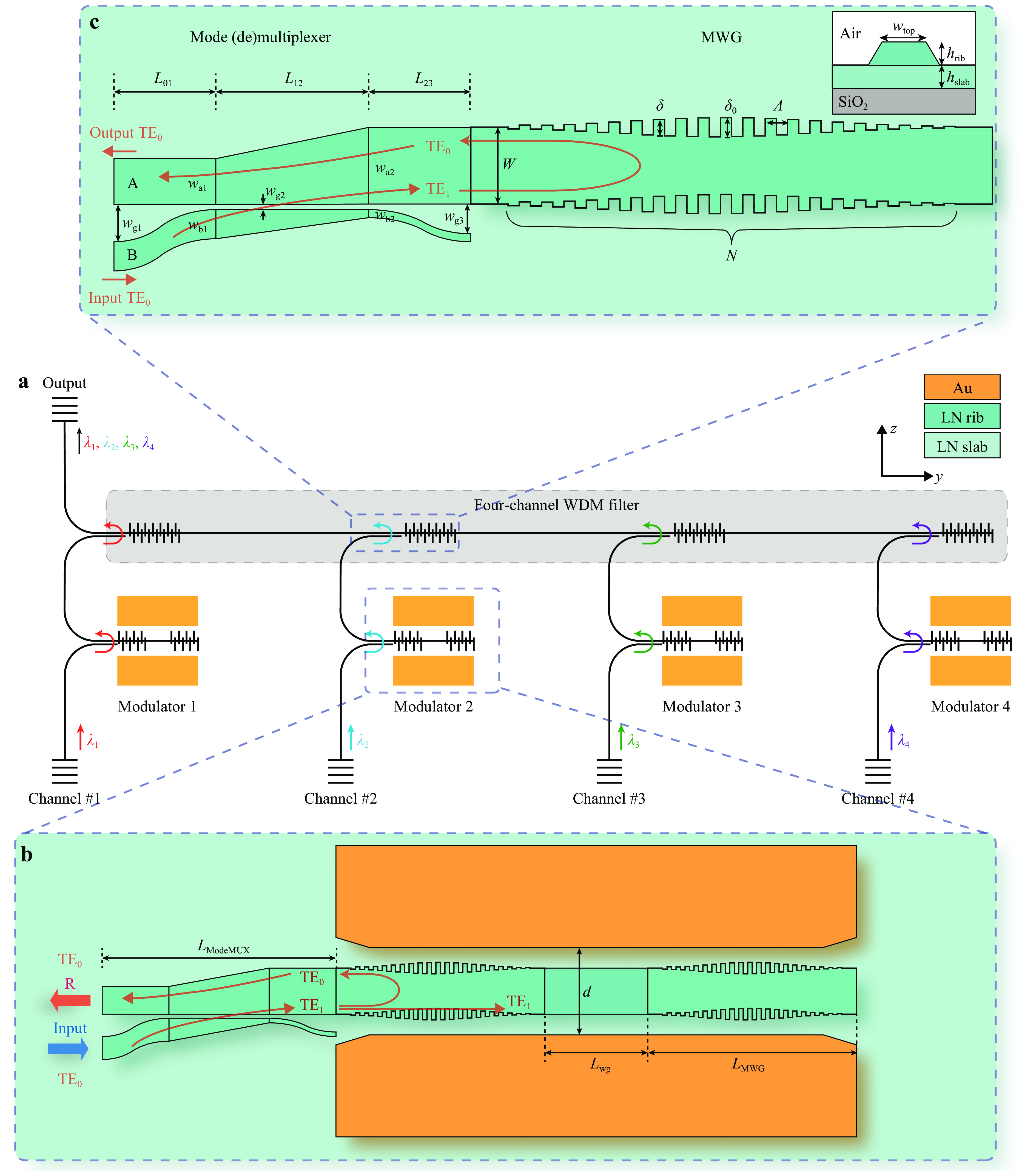
Ultra-compact lithium niobate photonic chip for high-capacity and energy-efficient wavelength-division-multiplexing transmitters
 Published , Published online: 29 May 2023 , doi: 10.37188/lam.2023.013
Recently, high-performance thin-film lithium niobate optical modulators have emerged that, together with advanced multiplexing technologies, are highly expected to satisfy the ever-growing demand for high-capacity optical interconnects utilizing multiple channels. Accordingly, in this study, a compact lithium-niobate-on-insulator (LNOI) photonic chip was adopted to establish four-channel wavelength-division-multiplexing (WDM) transmitters, comprising four optical modulators based on ultracompact 2 × 2 Fabry-Perot cavities and a four-channel WDM filter based on multimode waveguide gratings. The fabricated chip with four wavelength channels has a total footprint as compact as 0.3 × 2.8 mm2, and exhibits an excess loss of ~0.8 dB as well as low inter-channel crosstalk of < –22 dB. Using this LNOI photonic chip, high-capacity data transmissions of 320 Gbps (4 × 80 Gbps) on-off-keying signals and 400 Gbps (4 × 100 Gbps) four-level pulse amplitude signals were successfully realized with the ultra-low power consumption of 11.9 fJ/bit.
-
Article
Feature size below 100 nm realized by UV-LED-based microscope projection photolithography
 Published , Published online: 16 November 2023 , doi: 10.37188/lam.2023.033
The demand for miniaturization and integration of optical elements has fostered the development of various micro- and nanofabrication technologies. In this work, we developed a low-cost UV-LED-based microscope projection photolithography system for rapid and high-resolution fabrication. This system can be easily implemented using off-the-shelf components. It allows for micro- and nanostructuring within seconds. By optimizing the process, a minimum feature size down to approximately 85 nm was successfully realized. In addition, investigations on fabrication of the same structures using both costly and economic microscope objectives were performed. Feature sizes below 100 nm can be stably achieved. The demonstrated approach extends the technology capabilities and may find applications in fields such as nanophotonics, biophotonics sensing and material science.
 Lianshan Yan is currently the Dean of the School of Information Science & Technology (SIST) and the Director of Center for Information Photonics & Communications (CIPC) at Southwest Jiaotong University, China. Prof. Yan is the author and co-author of more than 500 papers, four books and two book chapters. He holds thirteen U.S. patents and more than seventy Chinese patents. Prof. Yan is a Fellow of Optica (former OSA). He is the co-Editor-in-Chief of Light: Advanced Manufacturing (2020-). He received the IEEE Photonics Society Distinguished Lecturer Award (2011-2013) and IEEE LEOS Graduate Fellowship (2002). He was the co-chair or TPC member of more than fifty international conferences. He is also the winner of the National Science Fund for Distinguished Young Scholars of China, Chair Professor of CheungKong Scholars Program. He was the Chair of Optical Fiber Technology Technical Group of OSA (2015-2018) and an associate editor of IEEE Photonics Journal (2009-2015).
 Baohua Jia is a professor and Australian Research Council Future Fellow in School of Science at RMIT University. Before joining RMIT Baohua was the Founding Director of Centre for Translational Atomaterials at Swinburne University of Technology. Her research focuses on the fundamental light and nano-and atomaterial interactions. In particular her work on laser manipulation of two-dimensional materials has led to the design and fabrication of functional nanostructures and nanomaterials for effective harnessing and storage of clean energy from sunlight, purifying water and air for clean environment and imaging, spectroscopy and nanofabrication using ultrafast laser towards fast-speed all-optical communications and intelligent manufacturing. Prof. Jia has co-authored more than 260 scientific publications in highly ranked journals and prestigious international conferences. She has delivered more than 60 keynote/invited talks at international conferences and serves multiples professional committees. She has received numerous prizes and awards, including the ARC Future Fellow, DECRA and APD, Finalist for the Prime Minister’s Science Awards, Young Tall Poppy Science Award, and L’Oréal Australia and New Zealand for Women in Science Fellowship et al.
 Di Liang is currently a director in Alibaba Cloud, Alibaba Group. Prior that, he was a Distinguished Technologist at Hewlett Packard Labs, Hewlett Packard Enterprise where he led the advanced R&D of silicon and compound semiconductor integrated photonics for high-performance computing and emerging applications. During 2007-2009, he was a core member in the early-stage joint development of III-V-on-silicon heterogeneous photonic integration between the University of California - Santa Barbara and Intel. His research interests include III-V and silicon photonic devices and integrated circuits, heterogeneous and monolithic material integration, and nanofabrication technology. He has authored and coauthored over 250 journal and conference papers, 1 edited book, 7 book chapters, and was granted by 49 patents with another 55+ pending. He is a Fellow of Optica (former OSA), a senior member of IEEE, and associated editor of Optica: Photonics Research and IEEE: Journal of Quantum Electronics.
 Prof. David Moss has a career in research in academia, industry and government research laboratories in Canada, Japan and Australia. He was with the University of Sydney for over 15 years, the last 10 of which were with the ARC Centre of Excellence CUDOS. David still holds an honorary Professorial Fellow position with the University of Sydney. Professor Moss has over 700 publications including numerous articles in Nature family journals and conference papers with around 12000 citations and an h-index of 64. He is leading extensive international research networks in nanophotonics and other areas. David has been highly successful at winning ARC competitive research grants and has won a number of notable awards for his research including the 2011 Australian Museum Award and the Google Eureka Science Prize for Innovation. David is a Fellow of the Optica (former OSA) and the IEEE.
 Xi Xiao is the CEO of National Information Optoelectronics Innovation Center (NOEIC) of China, and the vice director of State Key Laboratory of Optical Communication Technologies and Networks (OCTN) at China Information and Communication Technologies Group Corporation (CICT). He was an associate professor of the institute of Semiconductors, Chinese Academy of Sciences till 2013. His present research interests include the Terabps-scale silicon-based photonic devices for telecommunications, datacom and interconnect applications, as well as their enabling fabrication and integration technologies. He has published over 120 peer-reviewed journal and conference papers, including Nature Communications, Advanced Materials, ACS Photonics, Photonics Research, IEEE JSSC, ECOC post-deadline paper、ECOC invited talk and OFC invited talk. He was a subcommittee member of CLEO, ACP, OECC, POEM, and currently working as a subcommittee member of OFC 2023 and the editor of Light: Advanced Manufacturing.

 Email
Email RSS
RSS