


-
Wavefront modulation in optical imaging systems is increasingly crucial in dynamic optics, particularly in addressing issues such as atmospheric turbulence and aero-optic effects1,2.
The core component of such systems is the wavefront corrector, which is typically implemented using a deformable mirror (DM). Existing deformable mirrors are typically actuated by stacked-piezoelectric actuators3, transverse piezoelectric plates4,5, electromagnetic actuators6,7, and micro electro-mechanical systems (MEMS)8, among others. MEMS actuators, owing to their compact size, enable the integration of DMs into small optical devices, such as microscopes. However, their limited deformation range and small optical apertures restrict their applications.
Electromagnetic actuators offer the largest strokes, enabling substantial deformations in large-aperture mirrors. Despite this advantage, their bulky size, high power consumption, and low precision pose significant limitations. Stacked piezoelectric actuators provide a balance between stroke and precision; however, they are constrained by complex structures and large volumes, which hinder their broader application.
Among these options, transverse piezoelectric plates have been extensively studied and applied owing to their notable advantages, including simple structure, compact size, and lightweight design9,10. Within this category, the unimorph piezoelectric deformable mirror (UPDM) represents the simplest and most significant application, owing to its structural efficiency and functional versatility.
The main structure of a UPDM comprises a reflector sheet (passive layer) and a piezoelectric transducer (PZT) sheet (active layer), which are typically bonded together using conductive adhesives that also serve as a ground electrode. On the opposite side of the active layer, a drive electrode array is designed to control the electric field distribution, inducing deformation in the PZT and, consequently causing the mirror to deform. Therefore, the fabrication of the drive electrode is a critical challenge.
Traditionally, each drive electrode is electrically connected to the drive circuit using a "jump wire," a silver wire that connects the electrode to the circuit. This method requires individual connections for a large number of drive units within a limited operating space, placing stringent demands on specialized processes and equipment11. Therefore, developing an alternative method to eliminate the need for cumbersome jump wires is essential. The flexible printed circuit (FPC) technique offers a promising solution12. However, in previous work, the processes of electrode preparation and electrical connection based on FPC technology were handled separately, increasing the complexity of UPDM manufacturing. Consequently, the fabrication and integration of electrodes with the corresponding drive circuit remain two major challenges in UPDM development.
In addition to manufacturing challenges, achieving precision control of UPDM remains an unresolved issue. Control accuracy directly determines the surface shape of the deformable mirror (DM), which significantly influences wavefront correction performance. Owing to the use of PZT sheets as actuators, the inherent nonlinear characteristics of piezoelectric actuators (PEAs) present a substantial barrier to precise UPDM control. Wavefront sensors (WFSs) are commonly employed to establish a feedback control loop13,14. A WFS is typically integrated into the optical path to measure the optical wavefront rather than the mirror’s direct surface deformation. This approach increases the complexity of the optical system. Moreover, the bandwidth of WFSs is significantly lower than the kilohertz-level bandwidth of piezoelectric actuators, limiting the dynamic wavefront correction performance of UPDMs. Furthermore, in applications where incorporating a WFS is impractical, such as in airborne imaging systems, closed-loop control based solely on the UPDM is essential. This approach enhances the stability, reliability, and control accuracy of the entire system.
A feasible solution to this problem is to integrate additional sensors within the deformable mirror (DM) to directly measure the displacement of each piezoelectric (PZT) actuating channel. This approach is easily implemented in large PZT stacks, where displacement can be measured using an integrated strain circuit affixed to the actuator15. However, in the simple and highly integrated structure of a UPDM, only a single piezoelectric sheet exists, rendering incorporating strain gauges or other local stroke sensors for constructing localized feedback control challenging.
Svetina et al. addressed this challenge by attaching 13 strain gauges and 13 discrete piezoelectric actuators to the back of a thin fused silica substrate to modify the mirror profile and acquire data on its local shape16. Similarly, Poyneer et al. built a 45 cm long X-ray DM with 45 actuators and 45 full-bridge strain gauges17,18. However, the difficulty of integrating strain gauges increases significantly as the number of drive channels grows. In addition to using strain gauges, Alcock et al. proposed an alternative approach by simultaneously measuring the optical surface of a bimorph mirror at multiple locations using an array of interferometric position sensors to resolve higher-order spatial deformations19,20.
However, all the aforementioned solutions rely on the large size of the DM, a critical prerequisite. For instance, the strain gauges used by Svetina et al. measured 22 mm in length and 8 mm in width16. The sensor probe employed by Alcock et al. was approximately 27 mm long and required a supporting fixture20. These methods are impractical for miniaturized systems. Moreover, the complex structures and additional costs associated with these solutions undermine the inherent advantages of UPDMs.
Constructing a feedback layer using strain gauges appears to be a feasible approach for addressing this key issue21. Another strategy involves modifying the electrode configuration of the PZT actuator layers. Stroke sensing can be achieved by leveraging both the direct and inverse piezoelectric effects22. In this method, two types of electrodes are required for each actuator channel. The central electrode for actuation, and an outer annular sensor electrode for collecting the piezoelectric charge. However, both the additional sensor layer and the complex electrode design increase the structural complexity of the UPDM and reduce deformation capability. Additionally, discretely designed driving and sensing circuits multiply the number of jump wires, further complicating integration within the limited space of the UPDM.
In this study, we propose a novel UPDM featuring a localized closed-loop control scheme. First, the driving electrodes, electrical connection, and structural integration are achieved in a single step through a combination of screen printing and flexible printed circuit (FPC) techniques, significantly simplifying the manufacturing process. Second, a localized closed-loop control method for the UPDM is introduced based on the piezoelectric self-sensing principle, eliminating the need for additional structures or sensing electrodes. The feasibility and effectiveness of the proposed method are experimentally validated.
-
In this section, an integrated structure for the UPDM is proposed by combining electrode fabrication and electrical connection into a single-step process.
This integrated design is achieved by combining FPC and screen-printing techniques. The FPC was designed to form the drive electrodes and establish electrical connections between the electrodes and external connectors. The proposed FPC features a two-layer structure (Fig. 1a). The bottom layer consists of bare copper foil patterned to create the drive electrode array, forming the drive unit configuration. Each drive electrode includes a via hole in the top layer to facilitate electrical wiring.
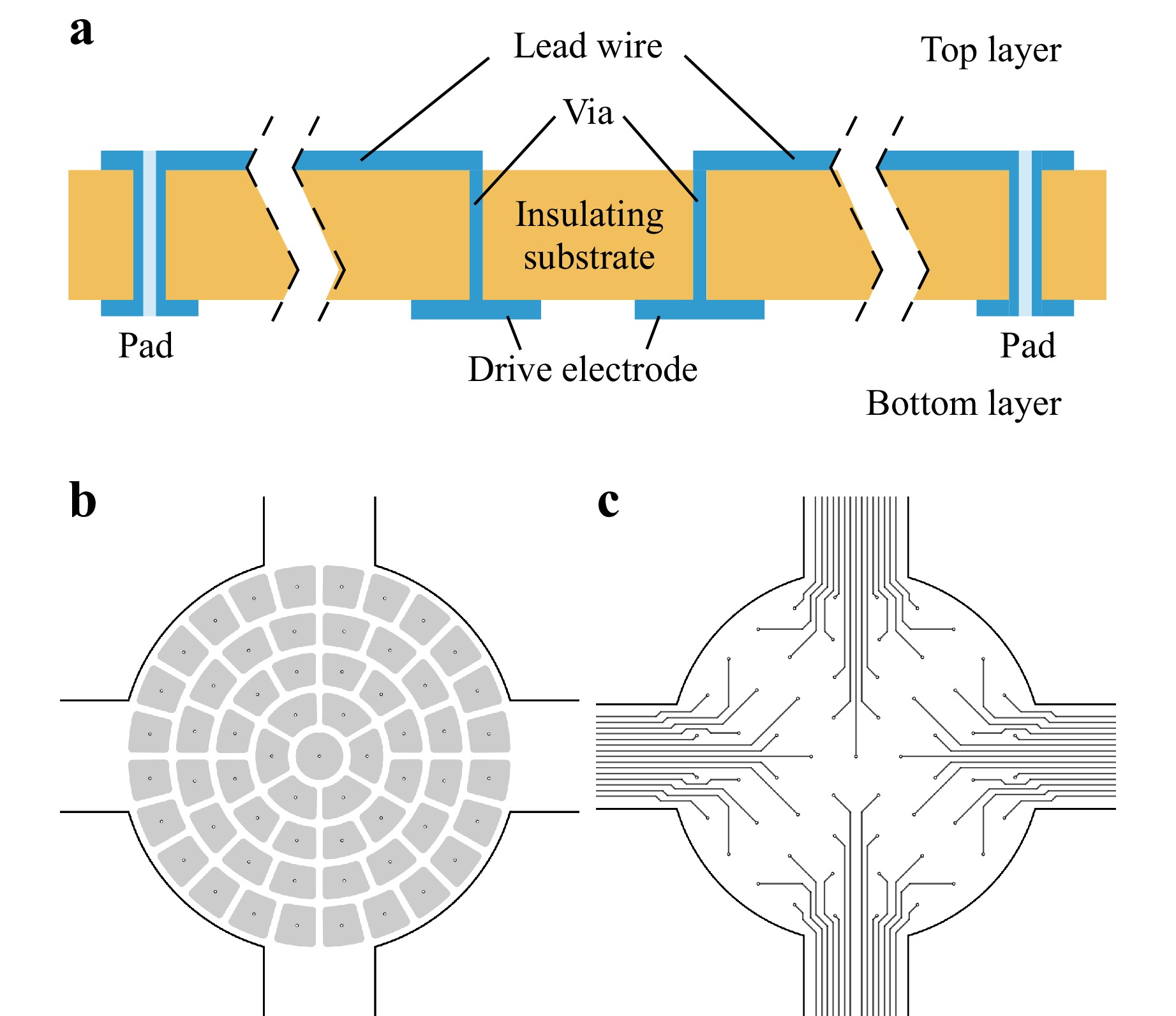
Fig. 1 Structure of flexible printed circuit (FPC). a Schematic diagram of the double-layer structure of the FPC. b Bottom layer of the example FPC illustrating the distribution pattern of the drive electrodes. c Top layer of the example FPC showing the electrical connection leads from each internal drive electrode to the external interface.
The top layer does not come into direct contact with the PZT film, providing sufficient space to route the drive electrodes while preventing short-circuits between units. Additionally, the top layer incorporates an array of pads that serve as electrical interfaces for the UPDM, enabling connections to external circuits.
Fig. 1b, c depict an example of this design. The bottom layer contains 58-sector-shaped electrodes along with a central drive electrode. This electrode arrangement is designed to better align with the optical aberrations described by Zernike polynomials. On the top layer, all the drive electrodes are divided into multiple segments and routed in different directions based on the “proximity principle.” The starting point of each routing line corresponds to the via connected to its respective drive electrode, while the endpoint terminates at the pad of the electrical connector (not shown in the figure due to space constraints).
The copper foil of the drive electrodes is connected to the PZT sheet to establish the final electrode configuration. In the proposed integrated structure, this connection is achieved using a screen-printing technique. The conductive adhesive is screen-printed onto the PZT sheet in a sector pattern that matches the copper foil layout on the bottom layer of the FPC.
This ensures precise alignment between the electrodes and the PZT, enhancing both electrical performance and structural integrity.
Through a single bonding operation, electrode fabrication, electrical wiring, and electrical connections can be completed simultaneously. Subsequently, by bonding the PZT sheet to the mirror using a conductive adhesive, the UPDM is easily manufactured. This novel integrated manufacturing approach significantly simplifies the production process.
The advantages of the proposed method are evident. First, the entire driving section of the UPDM is encapsulated into a single module using FPC, which directly and reliably integrates drive electrode fabrication and electrical connection. Second, the manufacturing process of the UPDM is streamlined by eliminating the need to create a drive-electrode array directly on the PZT film. Third, the bonding area between the FPC and PZT films exhibited a large surface electrode pattern, increasing the contact area and enhancing bonding reliability.
Fig. 2 illustrates the key principles of the proposed method and its fundamental manufacturing structure. As shown in Fig. 2a, the electrode pattern is screen-printed onto the PZT sheet. Fig. 2b shows the alignment and bonding relationship between the PZT sheet, conductive adhesive, and FPC. Fig. 2c displays the overall integrated structure of the fabricated UPDM.
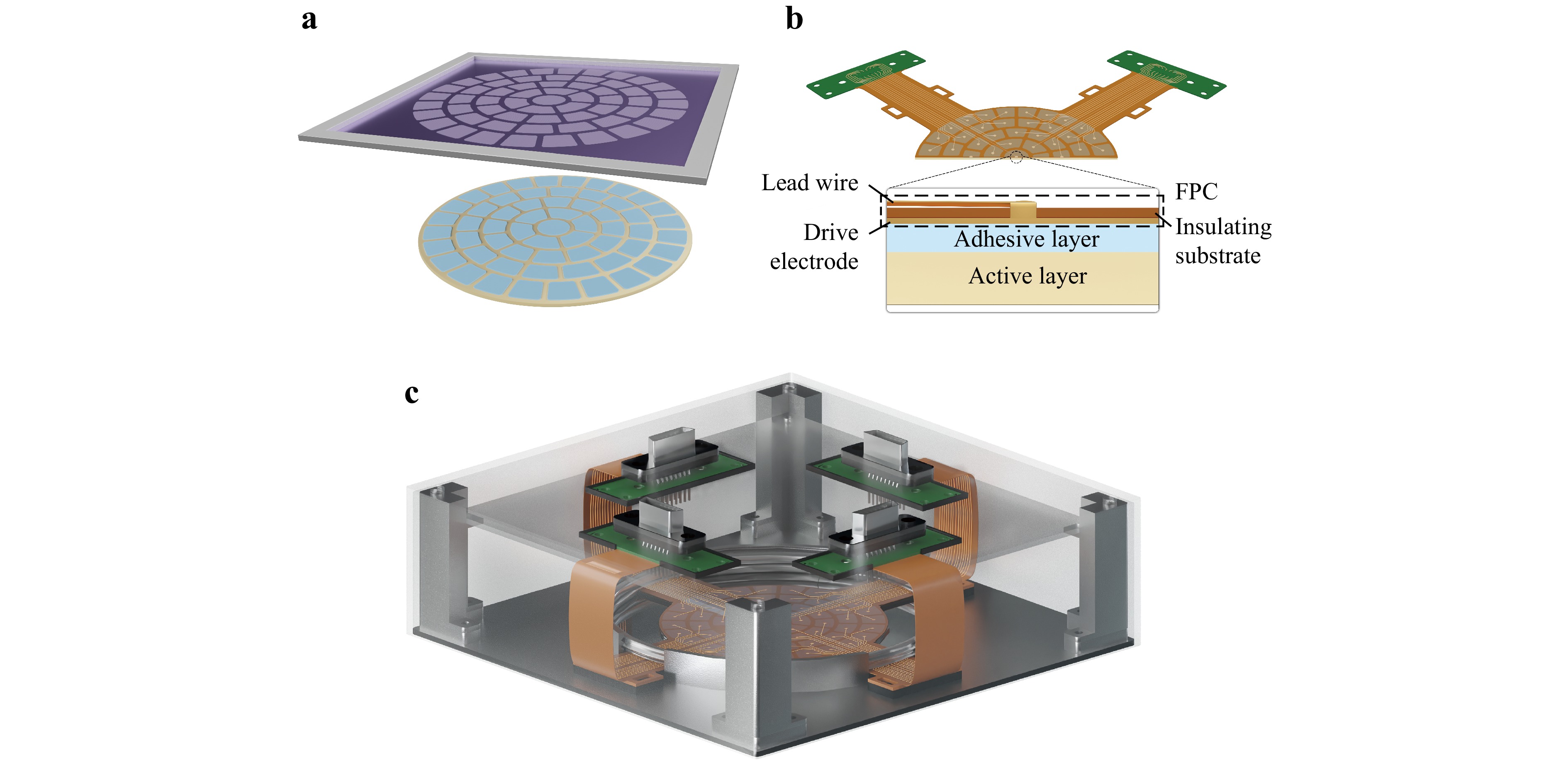
Fig. 2 Unimorph piezoelectric deformable mirror (UPDM) production processes and prototype. a Conductive silver adhesive screen-printed onto the surface of the piezoelectric (PZT) film following the drive electrode pattern. b Electrode array of the flexible printed circuit (FPC) aligned with the patterned conductive adhesive and bonded under preload to ensure reliable adhesion between the two layers. c Overall structure of the physical UPDM prototype.
The method proposed in this study, based on the FPC manufacturing process, enables the fabrication of electrode patterns and lead-outs on the FPC with high precision, surpassing the accuracy achievable through screen printing. Furthermore, by utilizing the multilayer structure of the FPC, lead-outs are designed on the top layer, separated from the electrodes on the bottom layer, thereby providing sufficient space for efficient routing.
During FPC manufacturing, an insulating layer is strategically applied to cover the lead-out sections to prevent electrical breakdown and discharge when there is a large potential difference between the lead-outs. Additionally, the combination of screen printing for manufacturing the conductive adhesive layer and the use of conductive silver paste possessing the same conductivity as the FPC electrode pattern effectively mitigates bonding issues between the FPC and the piezoelectric ceramic.
The lead wire is not directly bonded to the piezoelectric ceramic. Therefore, even if there are alignment errors between the electrode patterns of the FPC and the screen-printed electrode during manufacturing, the design remains robust as long as the error does not exceed half the gap size between the electrodes. In practice, this tolerance is manageable based on prior manufacturing experience. The gap between the electrodes typically measures several millimeters. Using auxiliary tooling, under standard machining and assembly conditions, these alignment requirements can be fully satisfied, where conventional accuracy is in the range 10–20 μm.
The first-order characteristic frequency of UPDM using the drive-lead FPC is 1215.48 Hz, with the corresponding vibration mode illustrated in Fig. 3a; In contrast, the first-order characteristic frequency of the UPDM using a traditional lead FPC is 1131.23 Hz, with its vibration mode shown in Fig. 3b The increase of 84.25 Hz in the first-order characteristic frequency is attributed to the compact structure of the proposed method, which integrates the drive electrode directly into the FPC.
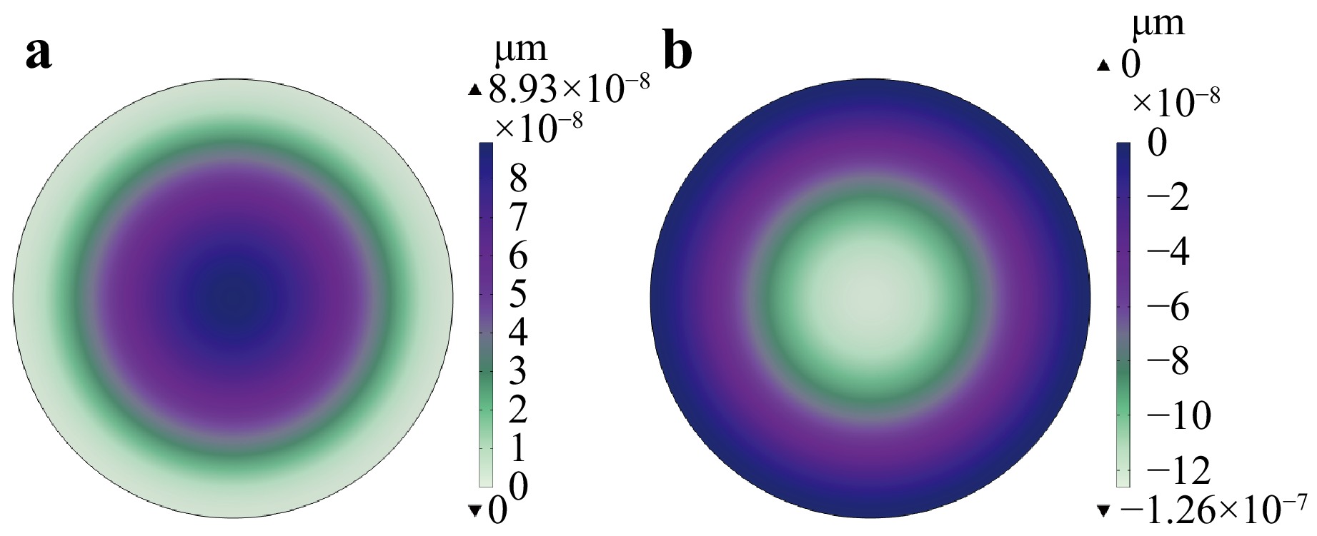
Fig. 3 Finite element analysis (FEA) results of the UPDM: a Vibration mode of the UPDM using only screen printing manufacturing method. b Vibration mode of the UPDM fabricated using the proposed integrated FPC method.
-
Self-sensing was established to construct a feedback control for the UPDM. Deformation measurement were performed based on the electro-mechanical model of the piezoelectric actuator (PEA), which serves as the driving element of the UPDM.
Within the electrical domain, the PEA behaves as a capacitor $ {C}_{pie} $ over a range of frequencies (Fig. 4). Nonlinear behaviors, such as hysteresis and creep effects, are modeled by a nonlinear element $ H $ associated with a corresponding voltage $ {v}_{H} $. The driving voltage $ {v}_{c} $ is the sum of $ {v}_{H} $ and $ {v}_{pie} $. The total charge q flowing into the PEA consists of the charge $ {q}_{pie} $ stored in the capacitor $ {C}_{pie} $ and the strain induced charge $ {q}_{\delta } $ generated by the piezoelectric effect.
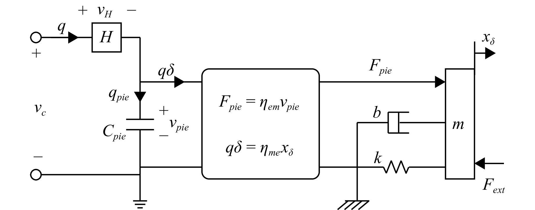
Fig. 4 Electro-mechanical model of piezoelectric actuator (PEA).
In the mechanical domain, the PEA is modeled as a lumped mass–spring–damper system, where $ k $ and $ b $ represent the spring constant and damping coefficient of the PEA, respectively. The application of $ {v}_{pie} $ induces a driving force $ {F}_{pie} $ through the inverse piezoelectric effect. This force acts in conjunction with the external mechanical force $ {F}_{ext} $ applied to the actuator, resulting in the deformation of the PEA by a displacement $ {x}_{\delta } $. According to the piezo-electric effect, the induced strain in the piezoelectric material generates a corresponding charge $ {q}_{\delta } $.
In a frequency range significantly lower than the fundamental resonance of the PEA, the electro-mechanical behavior can be modeled using a second-order model:
$$ \left\{\begin{array}{l}m{\ddot{x}}_{\delta }+b{\dot{x}}_{\delta }+k{x}_{\delta }-{\eta }_{em}{v}_{pie}={F}_{ext}\\ {{C}_{pie}v}_{pie}+{\eta }_{me}{x}_{\delta }=q\end{array}\right. $$ (1) Notably, the nonlinear operator $ H $, representing hysteresis and creep effects, is not included in Eq. 1 because it does not affect the liner relationship between $ {x}_{\delta } $ and $ q $.
The self-sensing method aims to determine the displacement $ {x}_{\delta } $ of the PEA by measuring the strain-induced charge $ {q}_{\delta } $, eliminating the need for external sensors. However, directly measuring $ {q}_{\delta } $ presents challenges owing to its low signal-to-noise ratio, which results from the small magnitude of strain-induced charge and inherent electronic imperfections Converting this small charge into a usable voltage, for feedback in the control loop, is therefore, complex.
These challenges were addressed by implementing a total-charge sensing scheme. Given the linear electromechanical properties of the PEA, $ {v}_{pie} $ can be assumed to have a linear relationship with $ {x}_{\delta } $. As shown in Eq. 1, there is also a linear relationship between the total charge $ q $ and the strain $ {x}_{\delta } $. This relationship enables the total charge to be utilized effectively for self-sensing. As the total charge $ q $ is the sum of the strain-induced charge $ {q}_{\delta } $ and the stored charge $ {q}_{pie} $, this approach is less sensitive to electronic imperfections and environmental disturbances, thereby enhancing robustness.
The self-sensing scheme was implemented as shown in Fig. 5. A reference capacitor $ {C}_{s} $, is connected in series with the PEA, and the output of the high-voltage amplifier AMP is applied across both components. Additionally a leakage resistor ($ {R}_{L} $) is connected in parallel with $ {C}_{pie} $. Although the effect of this resistor is typically negligible, it becomes significant at lower frequencies as it accounts for charge leakage from the PEA.
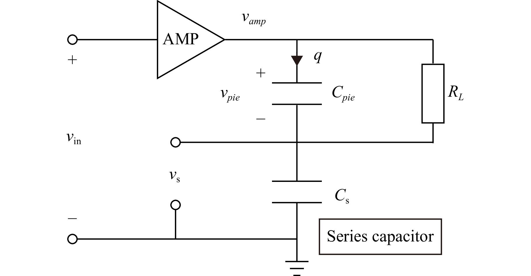
Fig. 5 Series capacitive self-sensing program.
Ideally, the charge stored in the reference capacitor $ {C}_{s} $ should be equal to that of the PEA, enabling direct access to the charge flowing through the circuit. The strain in the PEA can be estimated using the voltage $ {v}_{s} $, across the sense capacitor, which is proportional to the charge.
Notably, owing to the inherent imperfections of the PEA, charge leakage results in drift in both $ {v}_{pie} $ and $ {v}_{s} $ (Fig. 5). This drift cannot be fully mitigated through circuit design alone. This effect was compensated for by implementing a drift compensation strategy.
Feedback control can be established using the self-sensing method (Fig. 6). In this configuration, each channel of the UPDM is controlled independently. This control architecture provides an effective feedback mechanism, enhancing the stability and accuracy of the UPDM’s dynamic performance.
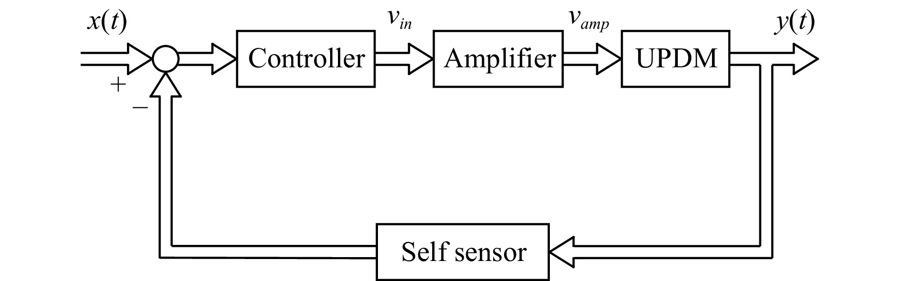
Fig. 6 Self-sensing feedback control diagram
By integrating the UPDM electrode construction proposed in this study with self-sensing feedback control methods, a broader range of application scenarios can be envisioned for UPDM. For instance, unlike traditional adaptive optics applications, in cases where the distribution of dynamic wavefront errors is known, precise simulation of wavefront errors can be achieved through closed-loop control using the UPDM’s own surface shape as feedback. This approach effectively compensates for wavefront error and enhances image quality in imaging applications. Although the aforementioned discussion focuses on the design results for a single channel, multichannel control can be readily realized through batch application owing to the structural consistency of each channel.
-
UPDM test system: Experiments were conducted to verify the feasibility of the proposed UPDM structural design and the effectiveness of the local closed-loop control scheme based on self-sensing. A UPDM prototype fabricated according to the proposed method was used for testing. The entire system was divided into two main components: electronics and optical (Fig. 7).
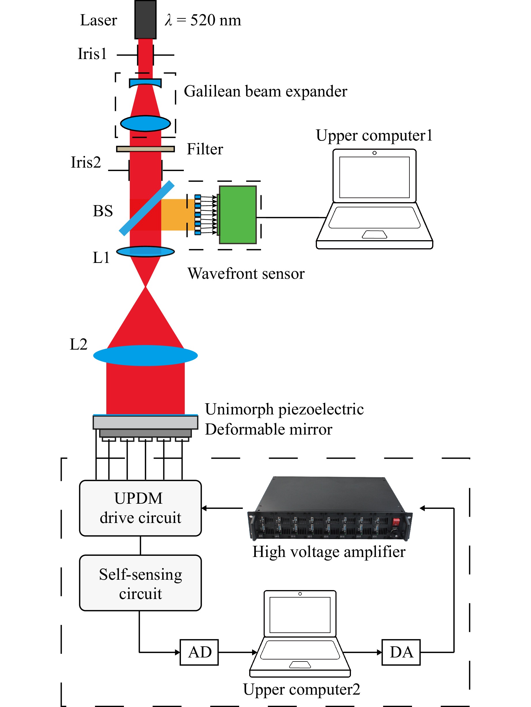
Fig. 7 Schematic of the UPDM test system.
Optical component: A collimated light source was used to produce a collimated beam which was then expanded using a Galileo beam expander. The expanded beam passed through a beam-splitting prism ensuring that the light spot covered the entire effective area of the deformable mirror. The wavefront sensor (WFS) and UPDM were positioned at the front and rear focal planes of the splitter, respectively. Changes in the UPDM surface were detected by the WFS and displayed on upper computer 1.
Electronics component: Control command was issued from upper computer 2, with control voltages generated via a digital-to-analog (DA) module. The control voltage was amplified 30 times using a high-voltage amplifier before being applied to the UPDM’s drive unit. The self-sensing circuits were connected in series with the drive units. Voltage values across the reference capacitor, representing the self-sensing signals, were acquired by an analog-to-digital (AD) module. The sampling frequency was set to 1000 Hz.
Influence function test: The UPDM comprises 59 drive electrodes within a 2-inch diameter, arranged as illustrated in Fig.8a. A voltage of 150 V was applied directly to each drive unit. The corresponding mirror deformation were detected using the wavefront sensor. The responses of the central electrode and four concentric layers of sector-shaped electrodes located in each quadrants are presented in Fig. 8b-f.
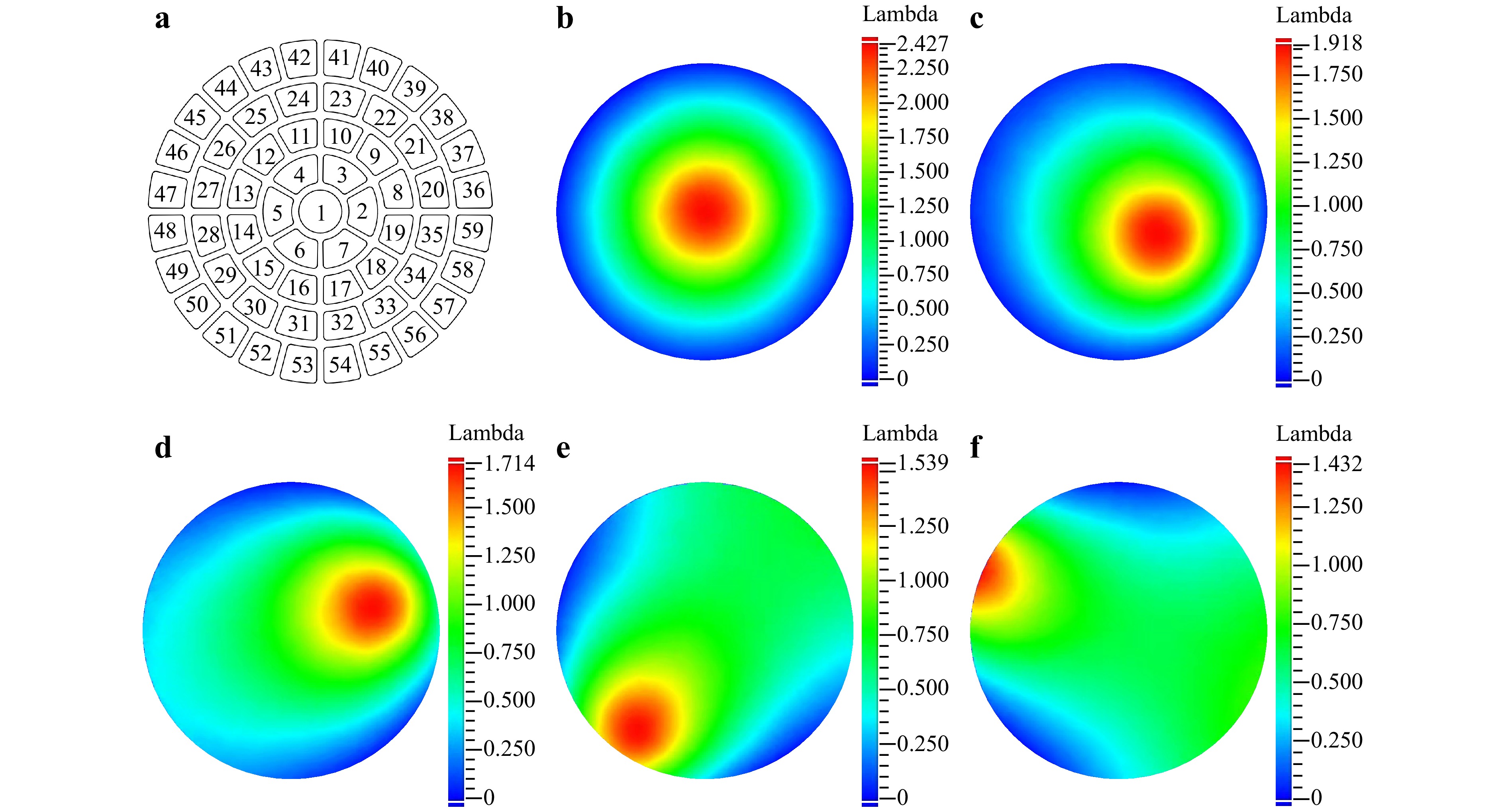
Fig. 8 UPDM drive unit distribution and typical influence functions. a UPDM prototype drive unit distribution comprising 58 drive units arranged in a fan-shaped four-layer row, with 6, 12, 16, and 24 units in each layer respectively, in addition to the central circular drive unit. b No.1 drive unit response result. c No.7 drive unit response result. d No.8 drive unit response result. e No.30 drive unit response result. f No.46 drive unit response result.
The experimental results demonstrate that the UPDM produces a measurable response for each activated drive unit.
The maximum deformation was observed in the central drive unit, reaching 2.427 $ \mathrm{\lambda } $.
The deformation amplitude decreased progressively with increasing distance from the center, which is attributed to stronger mechanical constraints on the outer drive units.
Despite these constraints, the outermost drive unit, still achieved a deformation of 1.432 $ \mathrm{\lambda } $. These results confirm the feasibility of the proposed UPDM structure and fabrication method, validating both its structural integrity and performance in dynamic wavefront correction applications.
UPDM self-sensing and drift compensation test: Self-sensing of the UPDM was verified using optical wavefront measurements. As described in the previous section, the self-sensing signal is subject to drift, which must be characterized and compensated for in practical applications. As the structure and characteristics of each drive channel are identical, the central electrode was selected for testing. By applying a half-cycle sinusoidal excitation signal with a peak value of 120 V and a frequency of 10 Hz to the UPDM central drive unit, the self-sensing signal is sampled as illustrated in Fig. 9. The results indicate that the self-sensing signal exhibits a linear drift overtime. Fitting the data with time $ \left(t\right) $ as the independent variable yielded a slope of −0.2974183 mV/s and a fitted R2-value of 0.993 indicating a strong linear correlation.
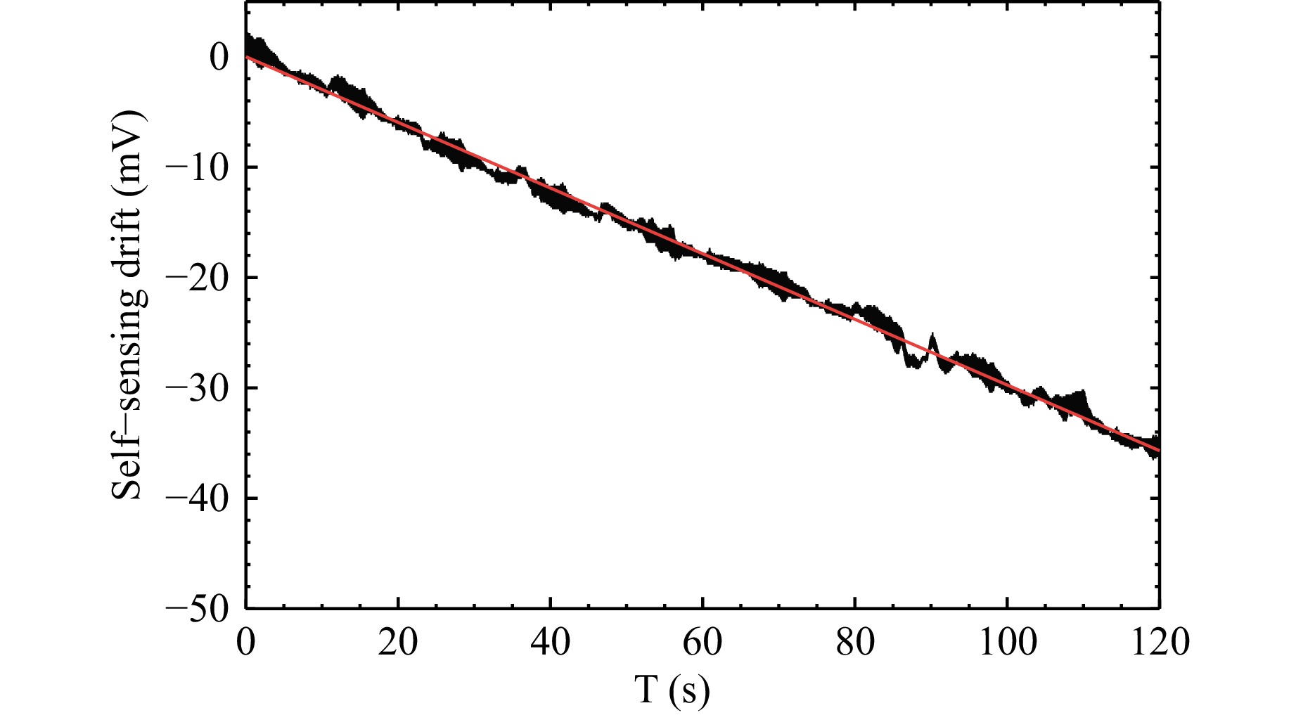
Fig. 9 Self-sensing data drift results over 120 s.
This linear drift characteristic can serve as a baseline for compensating for self-sensing signal drift. Additionally, defocus aberration coefficients obtained from WFS analysis were used to characterize local strains in the UPDM.
The defocus coefficient was chosen because it reflects the overall shape of the local region, rendering it a more robust indicator of local strain in the deformed mirror compared to the traditional peak-to-valley (P-V) value.
Notably, the WFS detects optical wavefront variations that are twice the magnitude of the UPDM’s surface deformation. However, because of the absolute linearity between the two, the strain of the mirror can be directly characterized using wavefront measurements. This is the physical quantity required to perform most applications, such as wavefront compensation. A voltage ranging from 0 to120 V was applied in 10 V intervals under quasi-static conditions with a signal frequency of 0.1 Hz. A wavefront sensor was used to obtain defocusing data, which were compared with the self-sensing signal. The results are presented in Fig. 10.
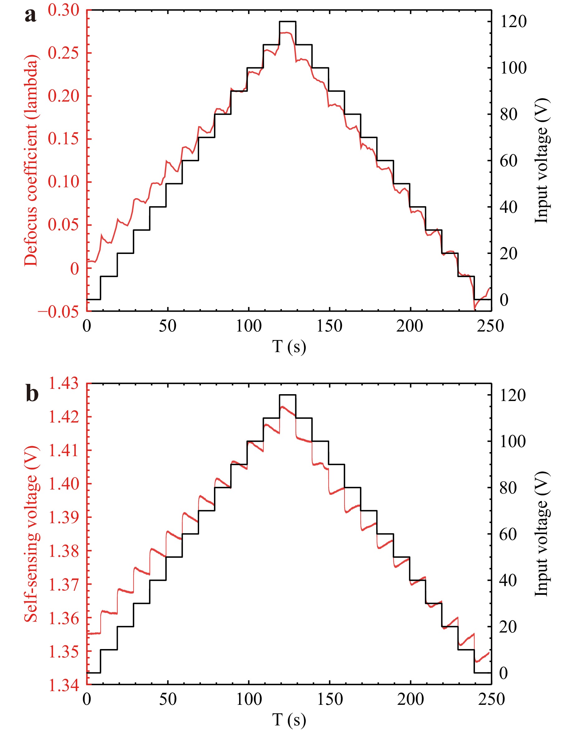
Fig. 10 UPDM open-loop control results. a Results of the defocus data (red line) in response to the input voltage (black line). b Results of the self-sensing data (red line) in response to the input voltage (black line).
The defocusing data and the self-sensing data correspond to the response of the UPDM central drive unit to the step signal, which demonstrates the feasibility of using the self-sensing method to control the UPDM. The defocus aberration coefficients obtained by WFS detection exhibit fluctuations due to environmental factors and the detection frame rate. Consequently, they do not display a clear step when the driving voltage changes. In comparison, the data obtained by self-sensing clearly reflect the effect of driving voltage changes. The self-sensing data were not entirely stable during the steady-state interval but exhibited time-dependent variations. During the rising phase, there was a negative change slope, whereas during the falling phase, there was a positive change slope. This is hypothesized to be a real deformation of the PZT rather than a drift of the self-sensing data, because a similar trend was observed in the defocusing data. This phenomenon can be attributed to charge leakage or the mirror elasticity effect, both of which require further investigation to fully understand their impact on the UPDM’s dynamic performance.
Sensing information corresponding to the defocus coefficients were obtained by processing the data as follows: The influence of the rising and falling edges of the step signal was eliminated by extracting the 8-s segment of each step response as steady-state data. These segments were then reorganized into a set of steady-state response data for further analysis. The defocused data $ x $ were fitted using multivariate linear regression with the amplified input voltage $ {v}_{amp} $, self-sensing data $ {v}_{s} $, and steady-state time parameter $ t $ as independent variables. The resulting equation is Eq. 2, with a calculated fitted R2-value of 0.9985.
$$ \left\{\begin{array}{l}x=a+b\cdot{v}_{amp}+c\cdot{v}_{s}+d\cdot t\\ a=-1.24506342426063\\ b=0.00180685945117831\\ c=0.926479402401152\\ d=-1.91575935137758\times {10}^{-4}\end{array}\right. $$ (2) The following analysis can be obtained from Eq. 2. The change in the UPDM face shape is caused by the amplified input voltage $ {v}_{amp} $, and this effect is characterized by coefficient $ b $. Accordingly, strain information can be obtained more accurately by adding $ c $ times the self-sensing data $ {(v}_{s}) $. The coefficient $ d $ corrects the time accumulation error, which is caused by self-sensing drifts that are not accurately modelled and compensated for, circuit temperature variations, etc. After applying Eq. 2, to process the sensing data, the results were compared with the defocused data. The results are shown in Fig. 11.

Fig. 11 Results of the processed sensing data fitting the defocused data.
The processed self-sensing data fit well with the defocused data collected by the WFS (Fig. 10). The fit is particularly good in the high-driving-voltage range, proving that the processed sensing signals can characterize the local strains of the UPDM and can thus be used as feedback information of the structural loop to achieve closed-loop control.
UPDM close-loop control test: Both Fig. 10 and Eq. 2 demonstrate that the response of the UPDM central drive unit strain to the control voltage is not strictly linear. This highlights the necessity of closed-loop control for UPDM. A model for the strain response of the UPDM drive unit was obtained by calibrating using a half-period sinusoidal excitation signal, as expressed in Eq. 3:
$$ f\left(t\right)=\left\{\begin{array}{*{20}{l}}4\mathit{sin}\left(20\pi t\right)&\left[0\right.,\left.0.05\right)\\ 0& otherwise\end{array}\right. $$ (3) where $ f\left(t\right) $ is in units of voltage, and $ t $ is in s. This low-frequency smoothly varying sinusoidal signal effectively minimizes the influence of hysteresis and yields the most accurate control voltage-strain correspondence.
After applying the control signal in Eq. 3 to the UPDM through the high-voltage amplifier, the sensing signal is acquired, calculated, and normalized within the range 0–4 V. By linking the maximum control voltage to the maximum strain as a model for closed-loop control through the aforementioned operations, a linear response of the UPDM can be achieved within this range.
Experiments were conducted to verify the specific performance of the closed-loop control of the UPDM using the self-sensing approach. The entire experimental process calculated the closed-loop feedback information using Eq. 2. Control commands were limited to 0–4 V to preserve a control margin and were then amplified 30 times by the high-voltage amplifier for application to the UPDM. This resulted in an amplified input voltage ranging from 0 to 120 V. A proportional-integration (PI) controller with control gains $ P=0.2 $ and $ I=0.3 $ was used as the control. Four step commands were applied to the UPDM, namely Step1, Step2, Step3, and Step4. The results of the closed-loop test are shown in Fig. 12. The UPDM successfully tracked the step signals and exhibited an extremely low steady-state error.
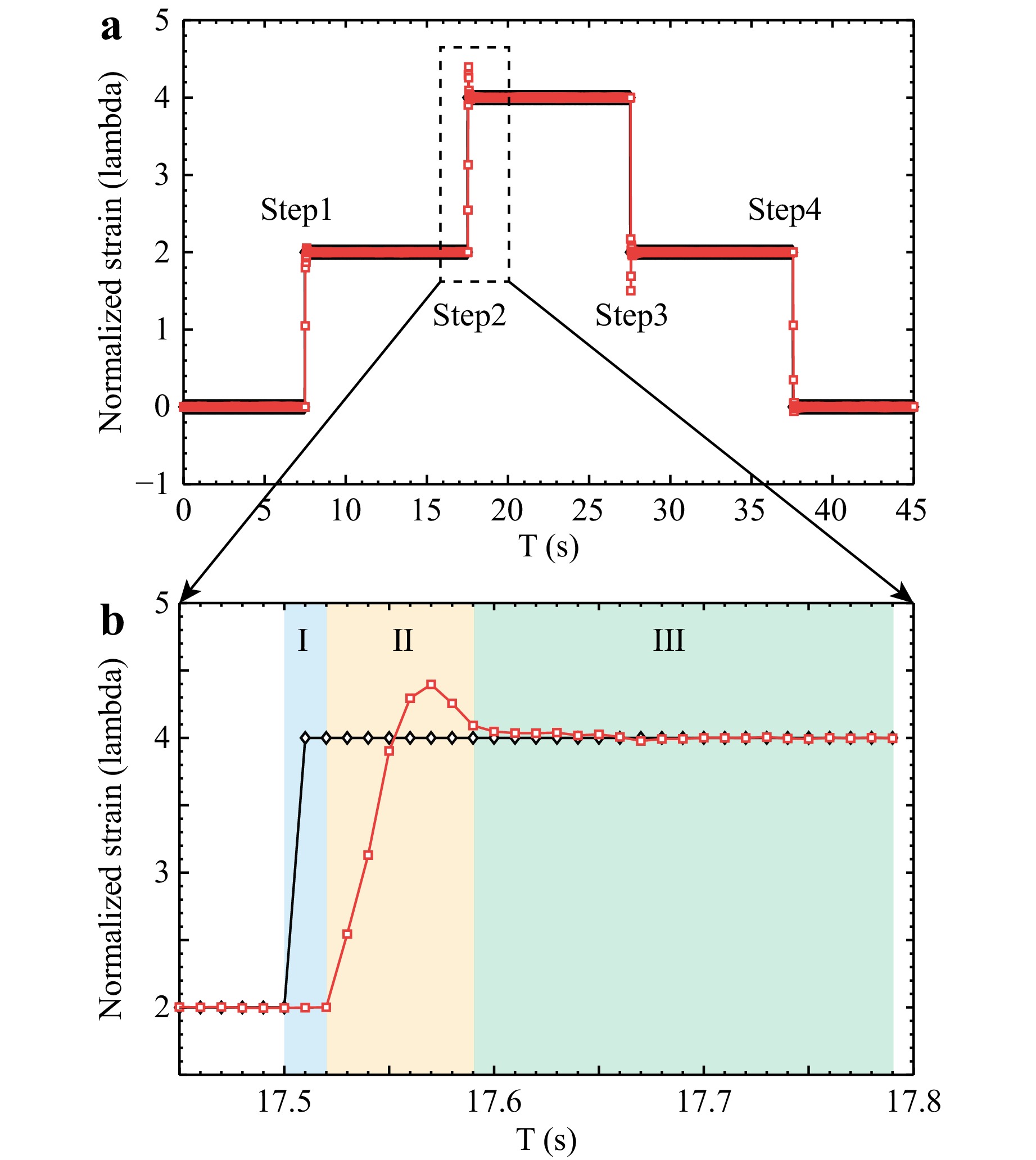
Fig. 12 UPDM closed-loop control results. a Full cycle response result. b Typical step response curve. There are three phases divided from left to right: the delay phase, the response phase and the stabilization phase.
A typical step-response result is shown in Fig. 12b. In region I, the response signal does not track the command signal due to the communication delay of the control loop, which is approximately 0.02 s. Region II is the response region, with a response time of 0.07 s and an overshoot of 9.92%. Subsequently, the system enters region III, which is characterized by a steady-state phase with a maximum relative error of less than 2%.
Table 1 summarizes the UPDM response to the four step commands, including the delay time $ {t}_{d} $, adjustment time $ {t}_{s} $, overshoot $ {\boldsymbol M}_p $, average of the steady-state relative errors $ \bar{e} $, and their RMS values $ {e}_{RMS} $. This shows that the closed-loop control of the UPDM using the piezoelectric self-sensing approach is effective, with small steady-state errors and regulation times. However, further optimization is necessary to minimize communication delays and reduce overshoot. These improvements can be achieved through refinements in the control circuitry and optimization of the control algorithm.
Step No. Step1 Step2 Step3 Step4 Mean $ {t}_{d} $/ms 20 20 30 20 22.5 $ {t}_{s} $/ms 100 70 110 150 107.5 Mp/% 2.62 9.92 24.88 5.68 10.78 $ \bar{e} $/10−4 1.04 1.18 −1.06 −5.49 −1.08 $ {e}_{RMS} $/10−2 0.16 0.12 0.16 0.28 0.18 Table 1. Step response results
-
This study presents a novel method for the fabrication of UPDM and sensorless closed-loop control. The driver unit array is integrated with electrodes and electrical connections simultaneously, which simplifies the manufacturing process while enhancing the bonding reliability. Furthermore, a piezoelectric self-sensing principle was introduced to enable strain measurements for closed-loop control without the need for additional sensors or electrodes.
The effectiveness of the proposed method was validated by comparing the calibrated deformation measurements obtained from the self-sensing system with data from the WFS. The comparison confirmed both the feasibility and accuracy of the self-sensing approach. A typical closed-loop control experiment was conducted using a PI controller to control a selected channel to track step signals. The mean steady-state error is of the order of 10−4. This result demonstrates the effectiveness of closed-loop control of the UPDM.
In the future, it will be desirable to investigate the nonlinear characteristics of PZT and accurately model the drift of self-sensing. Such efforts will improve the dynamic performance and decrease the overshoots in UPDM control.
-
Laser source: A collimated spot of diameter 3 mm was produced using THORLAB’s PL201 Compact laser modules as the light source. The laser source had a wavelength of 520 nm and a typical output power of 0.9 mW, which was filtered to match the incident power requirements of the wavefront sensor. THORLAB’s GBE05-A-5X Achromatic Galilean Beam Expander was used to expand the output spot of the light source so that its dimensions could meet the needs of the study.
Wavefront sensor: SID4 Ultra High-Resolution wavefront sensor was utilized to detect changes in the face shape of the UPDM. This WFS had a phase resolution of less than 2 nm RMS, enabling the accurate detection of the wavefront phase and recovery of changes in the mirror surface shape.
The aperture dimensions are 15.16 $ \times $ 15.16 mm2, which simplifies the construction of our optical path. However, its real-time processing frequency is very low at only 1 Hz. This prevented us from verifying higher-frequency control signals and resolving shorter dynamic processes.
-
This work was supported in part by the Strategic Priority Research Program of the Chinese Academy of Sciences (XDB1050000), in part by the CAS Project for Young Scientists in Basic Research (YSBR-066), in part by the National Science Foundation of China (T2122001), in part by the capital construction funds within the budget of Jilin Province (2023C030-6), and in part by the Youth Innovation Promotion Association of the Chinese Academy of Sciences (Y2021065). We also express our sincere gratitude to Dr. Shaoze Zhang, Prof. Qingyu Meng, and Prof. Kainan Yao for their invaluable support and contributions to this work.
Integrated structure and sensorless feedback control of unimorph piezoelectric deformable mirrors
- Light: Advanced Manufacturing , Article number: (2025)
- Received: 20 August 2024
- Revised: 23 February 2025
- Accepted: 26 February 2025 Published online: 12 March 2025
doi: https://doi.org/10.37188/lam.2025.025
Abstract: Deformable mirrors are essential dynamic wavefront compensation. Among the various types of deformable mirrors with different actuation mechanisms, the unimorph piezoelectric deformable mirror (UPDM) offers distinct advantages owing to its compact size and low cost. The two most critical challenges in UPDM are electrode fabrication and deformation control. This study proposes an integrated electrode fabrication and sensorless feedback control scheme for UPDM, which simplifies the manufacturing process and enhances its performance. The electrode array is created using silkscreen printing combined with flexible printed circuit board technology, integrating electrode fabrication and electrical connection into a single step. The desired mirror deformation is achieved by introducing a closed-loop direct deformation control method based on piezoelectric self-sensing. The feedback mechanism utilizes the local strain-induced charge generated by the piezoelectric plate, effectively addressing the nonlinear behavior of the piezoelectric material. Experimental results confirm the feasibility and effectiveness of the proposed method, with the maximum relative error in the steady state phase remaining below 2%.
Research Summary
Integrated manufacturing method of unimorph piezoelectric deformable mirrors
The unimorph deformable mirror, characterized by its simple structure and compact size, demonstrates significant application potential in wavefront error compensation for optical systems with stringent spatial constraints. Featuring a multilayer architecture, its piezoelectric actuator layer employs multiple driving electrodes to generate stress through the lateral piezoelectric effect, thereby inducing controlled deformation of the optical layer. Ping Jia from China’s State Key Laboratory of Dynamic Optical Imaging and Measurement now report manufacturing method of unimorph piezoelectric deformable mirrors. The innovative integration of screen printing and flexible circuit technologies enables the integrated fabrication and interconnection of electrodes on piezoelectric ceramic actuator layers, significantly streamlining the manufacturing process. Concurrently, a self-sensing methodology is developed that eliminates direct deformation measurement, instead employing charge detection circuitry coupled with estimation algorithms to determine the deformation magnitude of piezoelectric driving layers, thereby establishing closed-loop feedback control for mirror surface shaping. The team demonstrated the manufacturing process and control experimental results for the integrated unimorph piezoelectric deformable mirror.
Rights and permissions
Open Access This article is licensed under a Creative Commons Attribution 4.0 International License, which permits use, sharing, adaptation, distribution and reproduction in any medium or format, as long as you give appropriate credit to the original author(s) and the source, provide a link to the Creative Commons license, and indicate if changes were made. The images or other third party material in this article are included in the article′s Creative Commons license, unless indicated otherwise in a credit line to the material. If material is not included in the article′s Creative Commons license and your intended use is not permitted by statutory regulation or exceeds the permitted use, you will need to obtain permission directly from the copyright holder. To view a copy of this license, visit http://creativecommons.org/licenses/by/4.0/.

 DownLoad: