


-
Metamaterials are artificial materials composed of subwavelength artificial structure arrays, with extraordinary physical properties that are usually lacking in natural materials. Their material properties are based on artificial structures rather than the material components constituting their structures. They can flexibly manipulate electromagnetic (EM) waves; thus, attracting considerable interest1–5. By changing parameters, such as the effective permittivity and magnetic permeability of the material, the dispersion characteristics of EM waves can be adjusted. This can produce various functions and equipment that do not exist in nature as well as be used in practical applications3, such as invisibility cloaks6,7, focusing lenses8,9 and new antennas10. Although encouraging phenomena have been reported, metamaterials are often bulky and have the disadvantages of complex manufacturing, high losses, and strong dispersion11, which significantly limit their practical application. Recently, a two-dimensional form of metamaterials, metasurfaces, have been developed. Owing to the compatibility of metasurfaces with current integrated circuit processes and their advantages of small size, low thickness, low loss, simple manufacturing, and suitability for miniaturization, metasurfaces have now become one of the largest branches of metamaterials12. Metasurfaces are subwavelength structures arranged periodically or aperiodically on a two-dimensional surface with a powerful ability to manipulate EM waves. Metasurfaces are widely used in the microwave band for polarization conversion13,14, generating vortex beams15,16 and enhancing absorption17,18. To date, many metasurface-based functional devices with great application potential have been manufactured, such as holograms2,19, waveplates20, and polarization detection21–23, with great application potential. Further application of polarization multiplexing technology can effectively improve the control freedom and information capacity of metasurfaces while maintaining subwavelength thickness24. Based on these characteristics, multifunctional EM metasurfaces with complex multidimensional wavefront transformation capability25.
Recently, active metasurfaces have been developed that can flexibly adjust their EM properties to meet the needs of complex EM systems, with many remarkable achievements that can accomplish different functions under different conditions26–30. By loading active components controlled by the mechanical structure, active materials, voltage, and optical bias circuits onto the metasurface, the active metasurface can dynamically control the propagation characteristics of EM waves, such as the phase, amplitude, polarization state, etc31–34. With the development of metasurface technology, the theory of programmable digital coding metasurfaces (PDCMs) has been proposed, and the different states of the reflection and transmission responses are represented by a binary value of 0/15. The predesigned binary coding sequence is input into the metasurface controller to program the EM characteristics of the entire metasurface array and realize specific EM functions35,36, which have a wide range of applications in wireless communication37–39, holographic image40,41, and vortex beam42,43. However, to switch the state, most PDCMs are designed based on external excitation devices using the wired electronic control method, which requires multiple feeders to connect the circuit to the direct current power supply and metasurface interface, thereby increasing the complexity of the design system44. The emerging light control method can provide the driving signal in a non-contact manner through light, which has unique advantages, such as simplifying the system device and reducing signal crosstalk with unexpected effects45,46. It is possible to avoid the influence of bias circuits on EM transmission by replacing active components, such as positive-intrinsic-negative (PIN) diodes with photoresistors47.
Currently, intelligent components are developing rapidly towards intensification, miniaturization, etc., which increases the requirements for the integration of metasurfaces48. However, most coding metasurfaces are limited to adjusting one or two polarized EM waves, which cannot meet this requirement. Therefore, it is necessary to explore a new PDCM paradigm to overcome this limitation and achieve the purpose of dynamically adjusting multiple polarized EM waves. In this study, an integrated paradigm for spin-decoupling PDCM based on a light emitting diode (LED) array is proposed, as shown in Fig. 1, which independently manipulates the wavefront of the orthogonal circularly polarized (CP) wave in the co-polarization reflection channel and orthogonal linearly polarized (LP) wave in the co- and cross-polarization reflection channels. The paradigm completely embeds the photoresistor as part of the meta-atom and uses a computer to convert the coding sequence into a base 16 data frame, which is input to the LED array control board to control the on-off state of the LED array lamp beads. The LED array lamp beads correspond to the meta-atom one by one, which can separately change the photoresistor value to achieve the purpose of adjusting the reflected phase in different channels and customizing the far-field radiation. This study enhances the freedom of metasurface design and improves the adaptability of metasurfaces in practical applications. Furthermore, it can improve the integration degree of intelligent control metasurfaces, which lays the foundation for their development, provides a new direction, and has broad application prospects in the fields of mobile communication, information transmission, wireless coverage blindness, and adaptive intelligent perception.
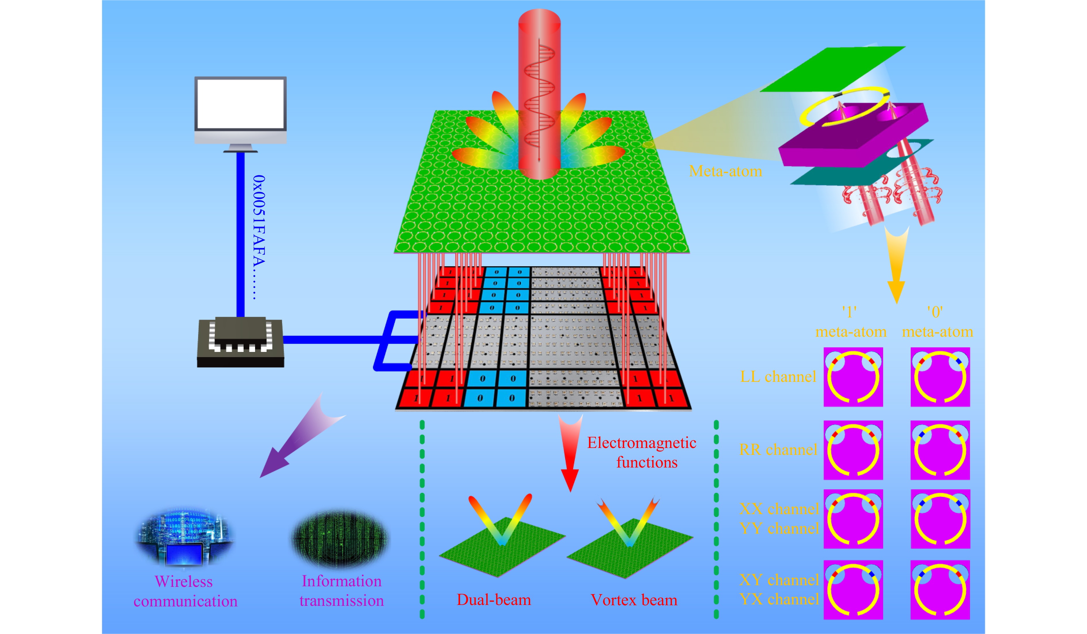
Fig. 1 Schematic diagram of the principle of spin decoupling PDCM and its application.
-
The GT36516 photoresistor value can reach 0.3 MΩ in the dark environment, which is in the off state at this time. However, with the gradual enhancement of the light intensity, it gradually drops to tens of ohms, which is in the on state at this time. Based on the characteristics of photoresistors in a dark environment, the metal split-ring resonator was truncated into three parts. In a light environment, the metal split-ring resonator is connected in its entirety. The photoresistor value was changed by adjusting the light intensity, which made it possible to change the resonant characteristics of the metal structure. Two photoresistors loaded on the meta-atom can produce four different states, which are represented by the codes '00', '01', '10', and '11'. The '0' or '1' in the first bit of the four codes indicates the off or on state of the left photoresistor, and the '0' or '1' in the second bit indicates the off or on state of the right photoresistor.
Using CST Microwave Studio software, the EM response of a well-designed meta-atom was simulated and optimized. Specifically, periodic boundary conditions are set to "unit cell" at four sides with CP waves normal incidence towards the -z direction. The loss resistance was used to simulate the photoresistor. In the simulation, meta-atoms in different photoresistor states can effectively achieve co-polarization reflection of orthogonal CP incident waves. According to the simulation results, the photoresistor can effectively truncate the induced surface current under an orthogonal CP incident wave, as shown in Fig. 2a, b. Therefore, the co-polarization reflection phases of the left-handed circularly polarized (LCP) and right-handed circularly polarized (RCP) waves can be modulated by adjusting the photoresistor state. As shown in Fig. 2c, e, the co-polarization reflection phase difference between state '11' meta-atoms and '10' meta-atoms is approximately $ \pi $ at 7.7 GHz, whereas the reflection amplitude is nearly equal under LCP-wave incidence. As shown in Fig. 2d, f, the co-polarization reflection phase difference between state '11' meta-atoms and '01' meta-atoms is approximately $ \pi $ at 7.7 GHz, whereas the reflection amplitudes are roughly equal under RCP-wave incidence. Therefore, the meta-atom can generate a 1-bit co-polarization reflection phase of the LCP and RCP waves by maintaining the on-state of one photoresistor and regulating the state of the other photoresistor.
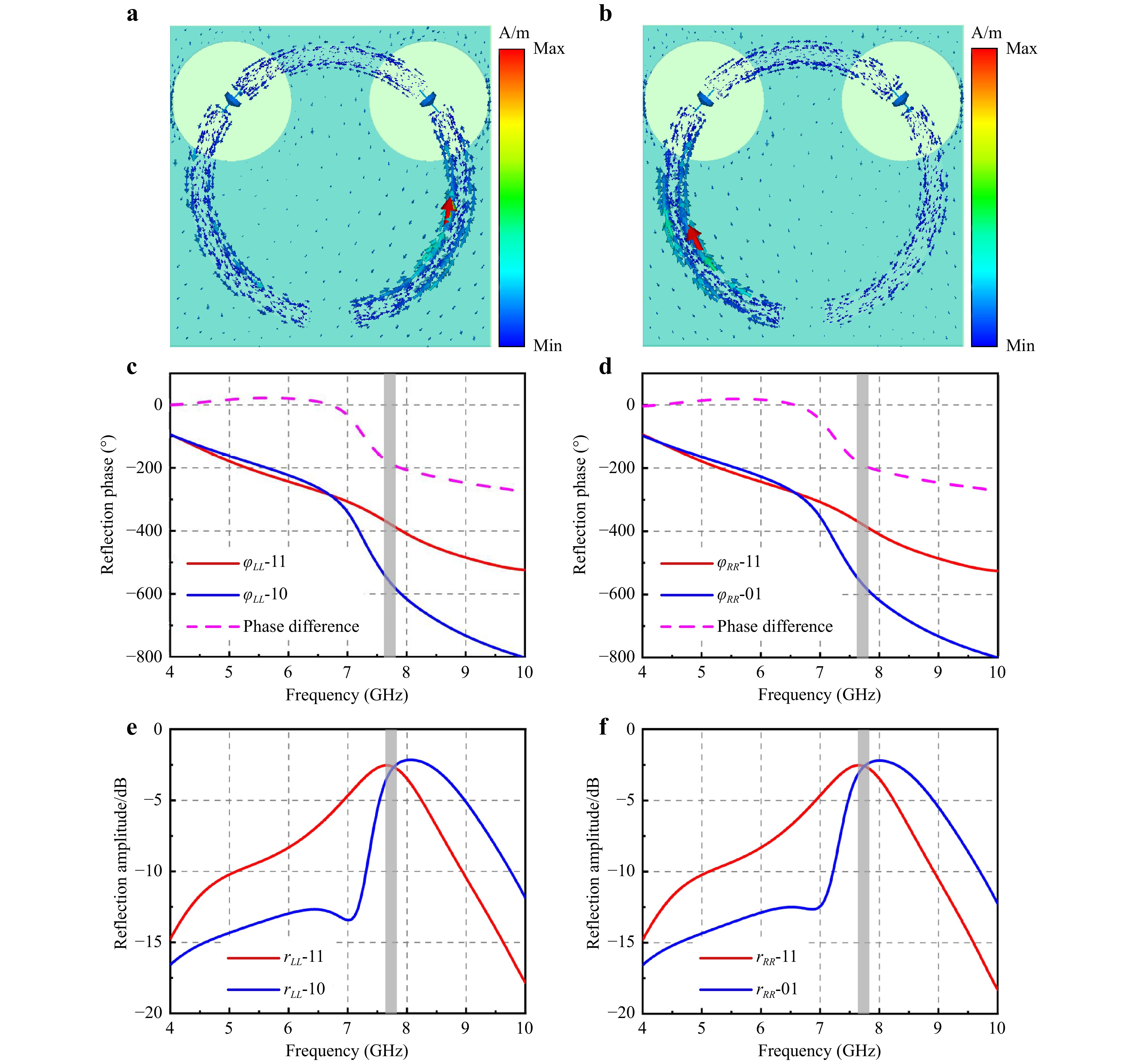
Fig. 2 Simulation results: a–b Surface current distribution of LCP and RCP under states '10' and '01', respectively; c–d Co-polarization reflection phase diagram; e–f Co-polarization reflection amplitude diagram.
In addition, the EM responses of the meta-atoms under LP-wave incidence were analyzed based on the Jones matrix (see Supplementary Information Note S1 for more details). By adjusting the states of the left and right photoresistors, the meta-atom can reflect the LP wave as a co- or cross-polarization wave. According to (S15) and (S16) in the Supplementary Information, by adjusting the photoresistors on the left and right sides to the same state, the meta-atom can realize the purpose of reflecting the LP wave into a co-polarization wave, thereby generating a 1-bit co-polarization reflection phase. Similarly, it can realize the purpose of reflecting the LP wave into a cross-polarization wave by adjusting the photoresistors on the left and right sides to different states, thereby generating a 1-bit cross-polarization reflection phase.
The photoresistor is adjusted to the '11' and '00' states, at which time the phase difference of the meta-atom under x- and y-polarized waves incidence is approximately $ \pi $ at 10.5 GHz and 7.2 GHz, respectively, and the amplitudes of co-polarization reflection at the corresponding frequencies are approximately equal, as shown in Fig. 3a, c and e. The photoresistor was adjusted to the '10' and '01' states, at which time the phase difference of the meta-atom under x- and y-polarized waves incidence was approximately $ \pi $ at 7.8 GHz, respectively, and the amplitudes of the co-polarization reflection at the corresponding frequencies were approximately equal, as shown in Fig. 3b, d and f. Based on the above simulation results, it was verified that the designed spin-decoupling meta-atom could effectively implement 1-bit digital phase modulation in two CP channels and four LP channels.
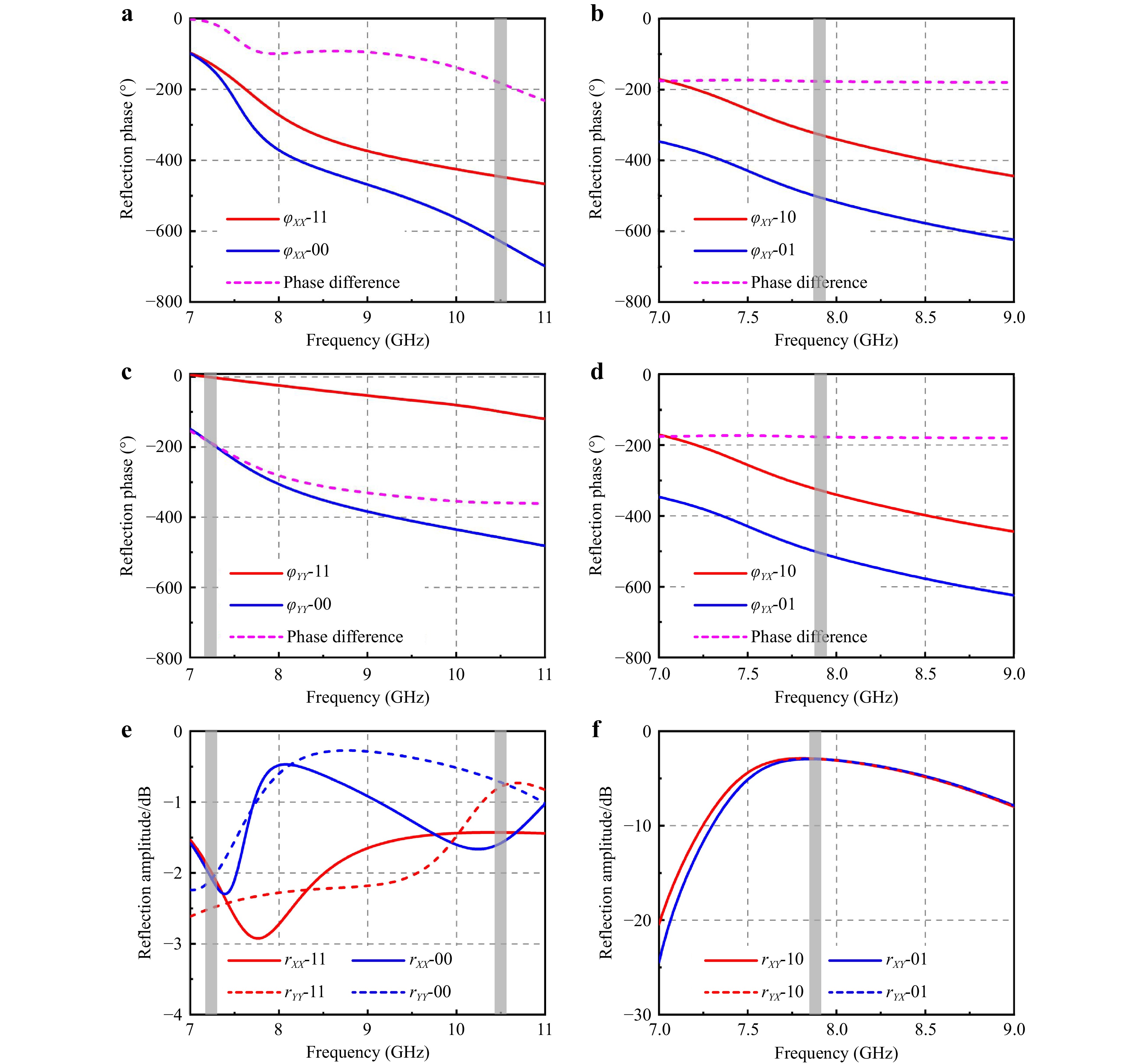
Fig. 3 Simulated co- and cross-polarization reflection coefficients under LP-wave incidence: a–d Reflection phase diagram; e–f Reflection amplitude diagram.
-
Based on the above design and analysis of the proposed spin-decoupling programmable meta-atom, a PDCM composed of 18 × 18 meta-atoms is constructed, which can independently manipulate the wavefront of the orthogonal CP wave in the co-polarization reflection channel and orthogonal LP wave of the co- and cross-polarization reflection channels to tailor EM functions. This study employed two common EM functions for verification: a dual beam and a vortex beam. The PDCM coding sequence was calculated according to different EM function theories (see Supplementary Information Note S2 for more details).
To make the simulation results more convincing, different parameters were set for different reflection channels for verification. In the dual-beam scheme, different coding periods are set, where the LL channel period is $ M = 2 $, RR channel period is $ M = 3 $, XX channel period is $ M = 4 $, YY channel period is $ M = 5 $, XY channel period is $ M = 6 $, and YX channel period is $ M = 7 $. The specific coding sequences are shown in Fig. 4a-f, respectively, with red representing the code '1' and blue representing the code '0'. According to (S19) in the Supplementary Information, the beam deflection angles of the different channels were calculated to be 37.5°, 23.9°, 12.9°, 15.1°, 11.5°, and 9.8°. Three-dimensional far-field scattering modes and RCS curves are shown in Fig. 4g-l. The scattering schematic shows that the PDCM produces two distinct scattered beams in six channels, and the simulated deflection angle of the generated beam is consistent with the theoretical results.
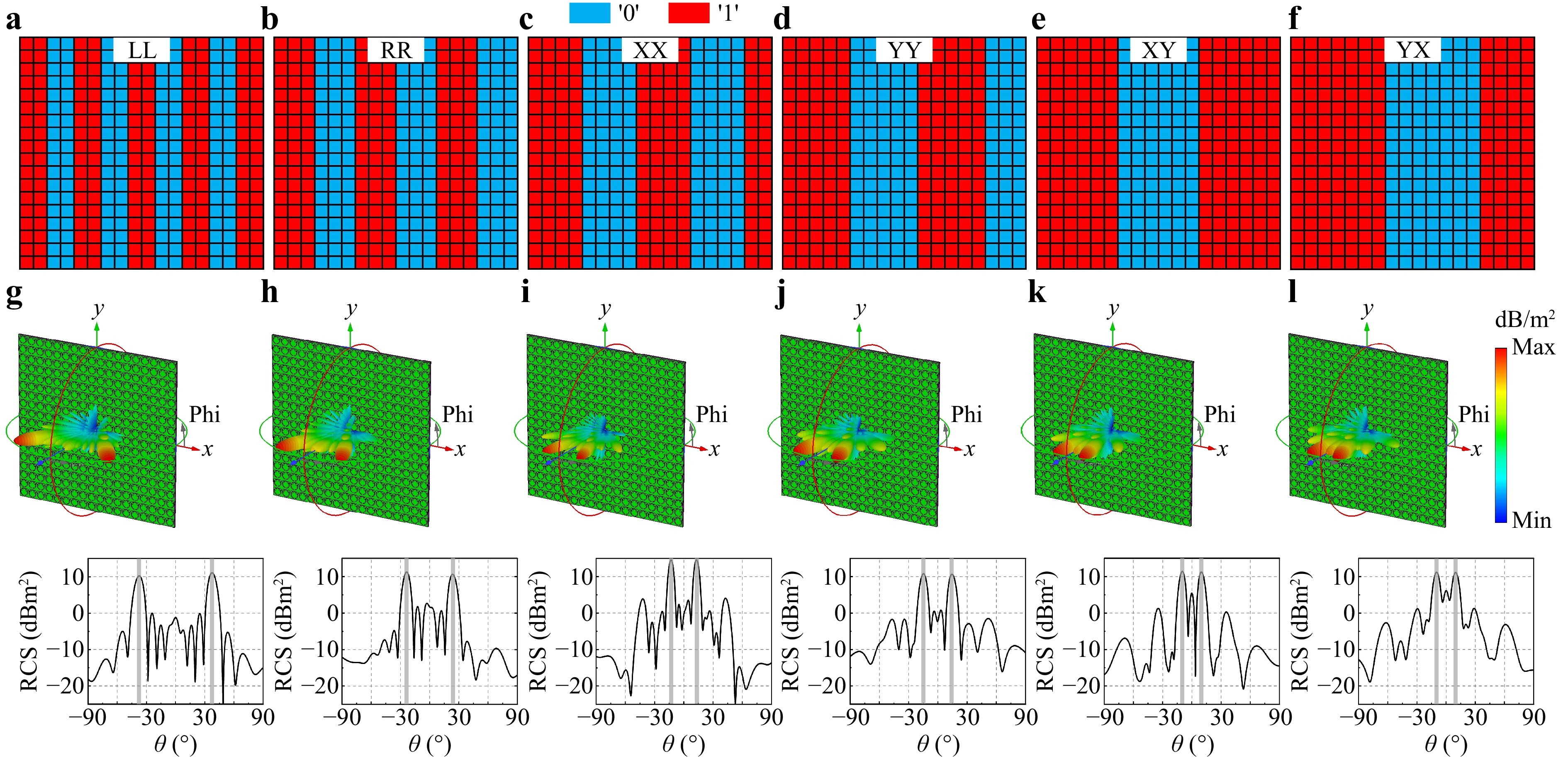
Fig. 4 Schematic diagram of simulation dual-beam reflection: a–f Coding sequence; g–l Three-dimensional far-field scattering mode and RCS curve.
Similarly, in the vortex beam scheme, with topological charge of ±2, different beam deflection angles are set, where the deflection angles of the LL and RR channels are $ \theta = {30^ \circ } $, the deflection angles of the XX and YY channels are $ \theta = {24^ \circ } $, and the deflection angles of the XY and YX channels are $ \theta = {18^ \circ } $. According to (S20) in the Supplementary Information, the specific coding sequences were calculated as shown in Fig. 5a-f, with red representing code '1' and blue representing code '0' Three-dimensional far-field scattering modes and RCS curves are shown in Fig. 5g-l. From the scattering schematic, it can be observed that the dual beam generated in each channel has a spiral-shaped wavefront structure, showing a ring-shaped intensity distribution map with a hollow center; the center nadir point of each beam is located near the pre-designed deflection angle, which is in line with the characteristics of the vortex beam. Therefore, the proposed PDCM can tailor the EM functions in six channels.
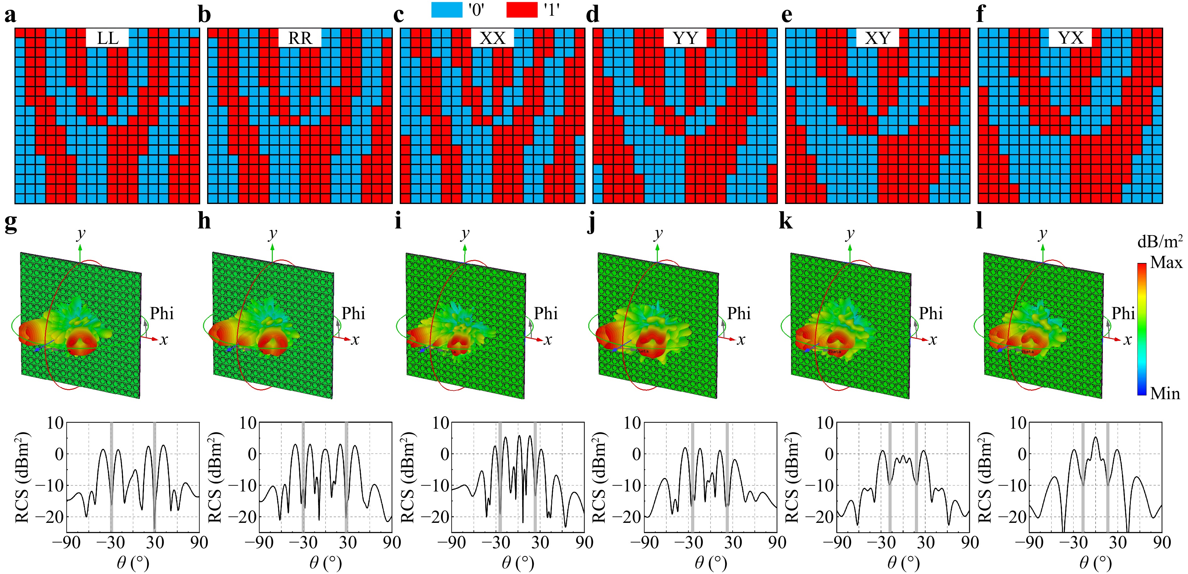
Fig. 5 Schematic diagram of simulation vortex beam reflection: a–f Coding sequence; g–l Three-dimensional far-field scattering mode and RCS curve.
-
In the experimental tests, the RR, YY, and YX channels were selected for verification. First, according to the coding sequence shown in Fig. 4a-f and 5a-f, the LED array was adjusted to realize a change in the photoresistor resistance. Subsequently, the dual-beam and vortex beams in the RR, YY, and XY channels were measured, and the actual measurement results are shown in Fig. 6a-f. According to the dual-beam measurement results, it can be observed that between −90° to 90°, the main lobe is eliminated, and there are two reflected beams on both sides, which is consistent with the characteristics of the dual-beam. According to the vortex beam measurement results, it can be observed that between −90° to 90°, the two beams generated have the characteristics of hollow center, which is consistent with the characteristics of vortex beam.
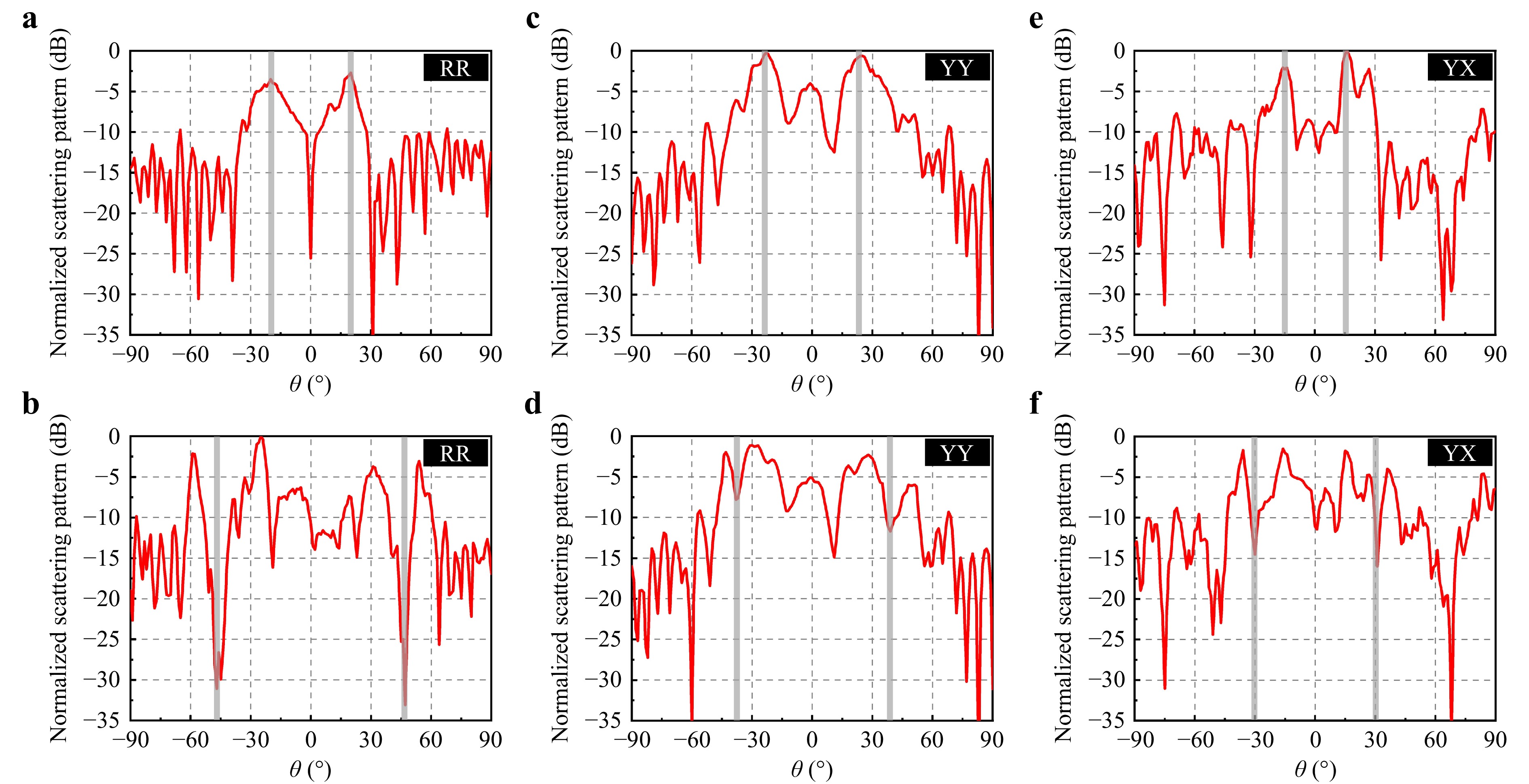
Fig. 6 Experimental results: a–b dual-beam and vortex beam measurements in the RR channel; c–d dual-beam and vortex beam measurements in the YY channel; e–f dual-beam and vortex beam measurements in the YX channel.
However, by comparing the simulated and experimental data, it was found that there was an error in the resonant frequency of the meta-atom. On one hand, this may be caused by the capacitance and inductance after the photoresistor package; on the other hand, it may be caused by processing errors, and the actual size of the second-layer metal structure is inaccurate with the simulation parameters, resulting in errors in the parameters (see Supplementary Information Note S3 for more details). According to the simulation results, the actual experimental S-parameter data were inconsistent with the simulated S-parameter data, owing to actual machining errors.
-
To realize dynamic adjustment of multiple-polarization EM waves, an integrated paradigm for a spin-decoupling PDCM based on an LED array is proposed. First, a spin-decoupled meta-atom was designed. Two identical photoresistors were embedded on both sides of the metal split-ring resonator, the resistance value of which was controlled using an LED array. The working principle was analyzed. The metasurface can independently manipulate the wavefront of the orthogonal CP wave in the co-polarization reflection channel and orthogonal LP wave in the co- and cross-polarization reflection channels. When the lamp bead is on, the photoresistor value decreases, which is encoded as '1', and when the lamp bead is dark, the photoresistor value increases, which is encoded as '0'. Using the CST software, when the photoresistor is adjusted to the '11' and '01/10' states, the 1-bit co-polarization reflection phase of the CP waves can be realized. When the photoresistor is adjusted to the '11' and '00' states, a 1-bit co-polarization reflection phase of LP waves can be realized. When the photoresistor was adjusted to the '10' and '01' states, a 1-bit cross-polarization reflection phase of the LP waves was realized.
According to the experimental results, the designed metasurface can customize the far-field scattering mode in six channels to tailor the EM functions. This verifies the feasibility and effectiveness of the integrated paradigm proposed in this study to control the scattering or radiation characteristics of EM waves in different channels. This study can improve the degree of integration of intelligent control metasurfaces, providing a new idea for the development of metasurface intensification and miniaturization with broad application prospects.
-
In this study, a dynamic spin-decoupling meta-atom consisting of a four-layer structure was carefully designed to manipulate different polarized incident waves, as shown in Fig. 7. The first layer was the top PI film (dielectric constant $ {\varepsilon _r} = 3.4 $, loss tangent $ \tan \delta = 0.001 $), which was used to provide mechanical support for the metal structure. The second structure is a metal split-ring resonator with an opening in a symmetrical position on the left and right sides to load two identical GT36516 photoresistors with photosensitive side facing down to sense light.
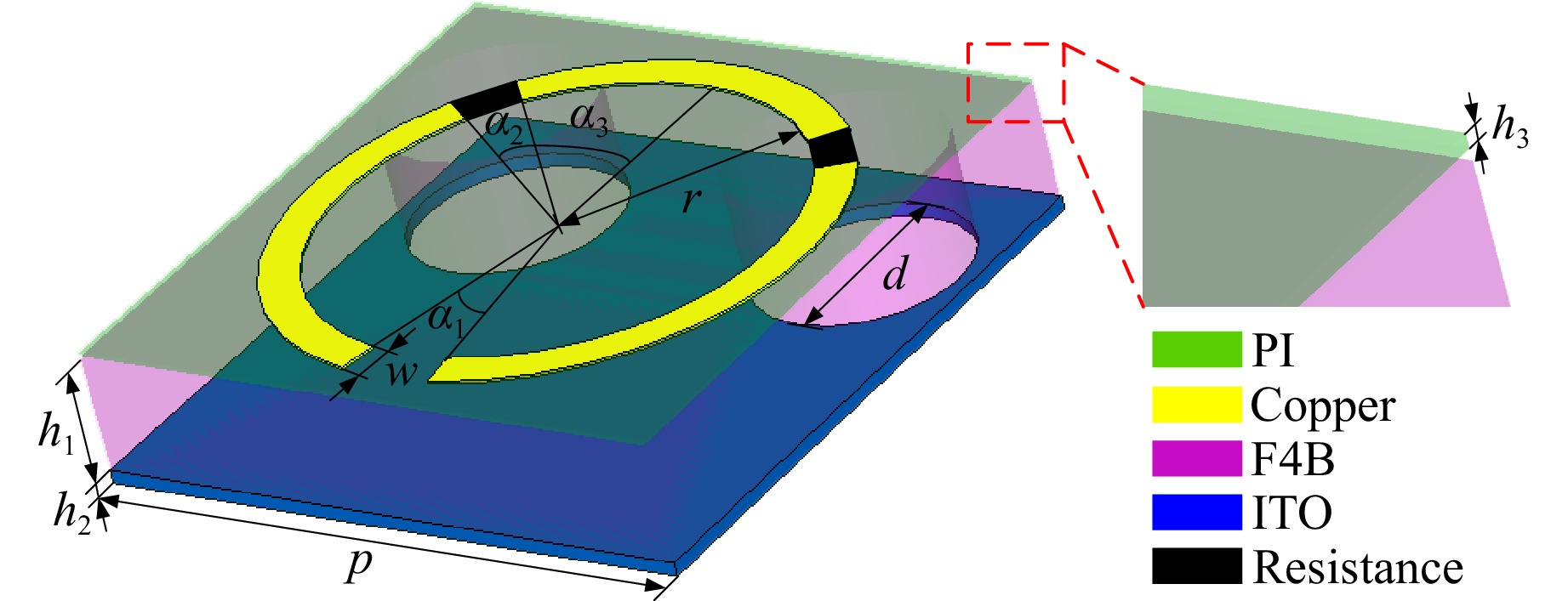
Fig. 7 Schematic diagram of dynamic spin decoupling meta-atom structure and geometric parameters.
The other layer structures are F4B dielectric substrate (dielectric constant $ {\varepsilon _r} = 2.65 $, loss tangent $ \tan \delta = 0.001 $) and conductive film ITO (sheet resistance 5 Ω), separately. The conductive film ITO is manufactured through sputtering transparent ITO on a PET (dielectric constant $ {\varepsilon _r} = 3 $, loss tangent $ \tan \delta = 0.06 $) substrate material. To achieve the purpose of control the meta-atoms through the LED array and ensure that the emitted light can adjust the photoresistor value, it is necessary to punch holes in the corresponding photoresistor positions on the dielectric substrate and conductive film ITO, as shown in Fig. 7.
The period of the meta-atom structure is $ p = 16\;{\text{mm}} $, inner diameter of the metal split-ring resonator is $ r = 6\;{\text{mm}} $, width is $ w = 1\;{\text{mm}} $, bottom opening angle is $ {\alpha _1} = 20^\circ $, and opening angles of the left and right sides are $ {\alpha _2} = 13^\circ $. The photoresistor deflection angle is $ {\alpha _3} = 43^\circ $. The hole diameter is $ d = 5.4\;{\text{mm}} $. The PI film thickness is $ {h_1} = 0.05\;{\text{mm}} $, dielectric substrate thickness is $ {h_2} = 3\;{\text{mm}} $, and conductive film ITO thickness is $ {h_3} = 0.175\;{\text{mm}} $. The thickness of the metal split-ring resonator was 0.035 mm.
-
To quantitatively illustrate the wavefront of the reflected wave, we considered a general metasurface composed of $ N \times N $ meta-atoms. When an EM wave incident is perpendicular to the metasurface, the far-field scattering function is
$$\begin{split}& f\left( {\theta ,\varphi } \right) = {f_e}\left( {\theta ,\varphi } \right)\;\sum\limits_{m = 1}^N \sum\limits_{n = 1}^N \exp \{ - j[{\varphi _{(m,n)}} \\&+ k{D_x}(m - 1/2)\sin \theta \cos \varphi + k{D_y}(n - 1/2)\sin \theta \sin \varphi ]\} \end{split}$$ (1) where $ {f_e}\left( {\theta ,\varphi } \right) $ is the mode function of the meta-atom; $ {\varphi _{(m,n)}} $ is the reflected phase of the meta-atom; $ k $ is the wave vector; $ {D_x} $ and $ {D_y} $ is the physical length of the meta-atom in the $ x $ and $ y $ directions; and $ \theta $ and $ \varphi $ are the pitch and azimuth angles, respectively, in any direction.
-
To further verify the practicality of the designed PDCM, different materials were carefully machined into samples according to the simulation model, and photoresistors were welded to the metal split-ring resonator, as shown in Fig. 8a. The 2835 lamp beads are integrated on an aluminum substrate to make an LED array to control the photoresistor value, as shown in Fig. 8b. In this study, serial communication was used to transmit signals and control the LED array. The different coding sequences were converted into base 16 data frames through a computer and output to the LED array control board through the computer USB port and USB converter, which was used to control the on-off state of each lamp bead on the LED array and change the photoresistor value (See Supplementary Information Note S4 for further details).
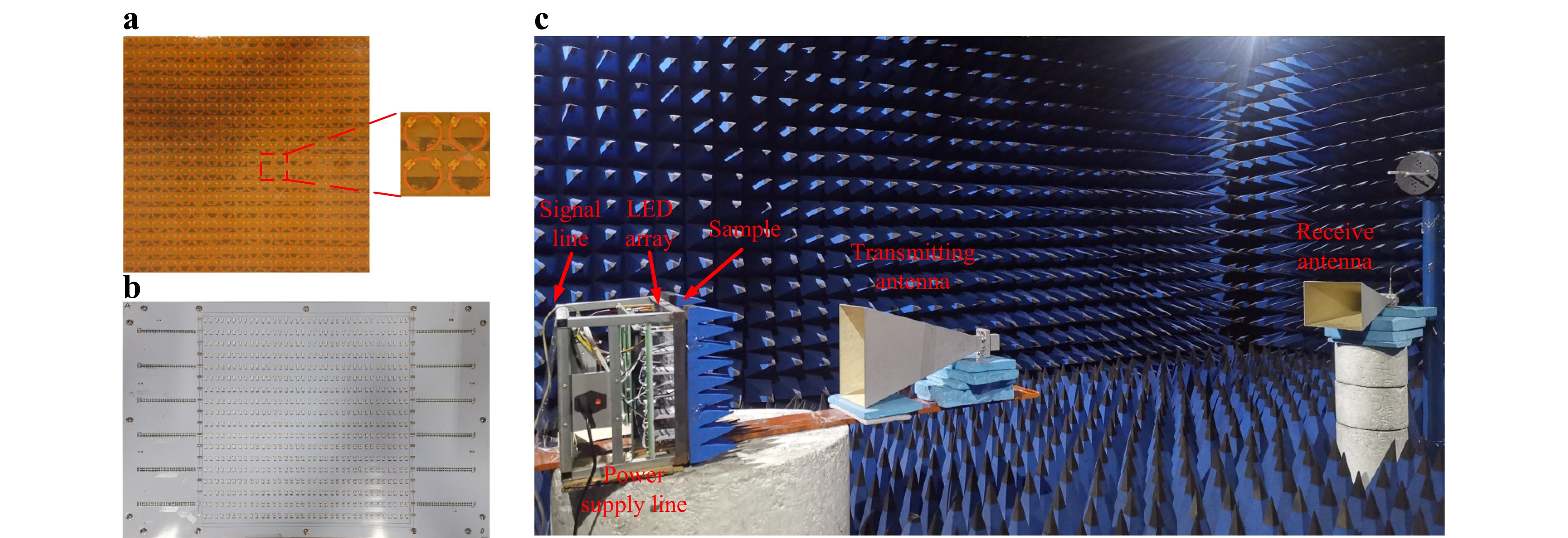
Fig. 8 a–b PDCM sample and LED array physical diagram; c Schematic diagram of the experimental setup.
-
In this study, 2835 lamp beads with wavelengths of 520 nm, 560 nm, 590 nm and 620 nm were selected for testing, and the photoresistor value under different wavelength light sources was obtained (See Supplementary Information Note S5 for more details). Based on the data presented in Table. S1, the photoresistor is sensitive to a 620 nm wavelength light source, and the resistance value can drop below 50 Ω.
-
Far-field experiments on the samples were performed in a microwave anechoic chamber. The experimental setup consisted of a vector network analyzer, horn antenna, and turntable mount. To measure the far-field scattering mode, an experimental sample and a pair of horn antennas were placed as shown in Fig. 8c. One horn antenna, which acts as a transmitti1ng antenna, is placed on a turntable with the sample and rotates with the sample, whereas the other horn antenna, which acts as a receiving antenna, is fixed at the far end. Initially, the two horn antennas faced the sample. According to the different polarization requirements, the horn antenna was rotated to measure the far-field scattering mode.
-
This work was supported in part by the National Key Research and Development Program of China under Grant 2022YFB3806200 and the National Natural Science Foundation of China under Grants 62101588 and 62201609.
Achiral light-controlled coding metasurfaces with multi-channel electromagnetic control
- Light: Advanced Manufacturing , Article number: (2025)
- Received: 28 June 2024
- Revised: 25 December 2024
- Accepted: 25 December 2024 Published online: 06 March 2025
doi: https://doi.org/10.37188/lam.2025.013
Abstract: Programmable digital coding metasurfaces (PDCMs) can manipulate electromagnetic waves with high degrees of freedom, significantly enriching metasurface designs. However, most PDCMs are limited to the control of a single polarization, which cannot meet the requirements of the high integration of intelligent components. To further improve the practicability and flexibility of metasurfaces, we propose an integrated paradigm for spin-decoupling PDCMs based on light emitting diode arrays that fully embed the photoresistor as a part of the meta-atom to independently manipulate the wavefront in different polarizations. As a proof of concept, PDCMs were simulated, fabricated, and measured to verify the feasibility and effectiveness of the proposed method. The functions of scattering and vortices are verified at different polarizations, demonstrating that the metasurface can tailor the EM functions in six channels. This study can improve the integration of intelligent control metasurfaces and lay a solid foundation for their development.
Rights and permissions
Open Access This article is licensed under a Creative Commons Attribution 4.0 International License, which permits use, sharing, adaptation, distribution and reproduction in any medium or format, as long as you give appropriate credit to the original author(s) and the source, provide a link to the Creative Commons license, and indicate if changes were made. The images or other third party material in this article are included in the article′s Creative Commons license, unless indicated otherwise in a credit line to the material. If material is not included in the article′s Creative Commons license and your intended use is not permitted by statutory regulation or exceeds the permitted use, you will need to obtain permission directly from the copyright holder. To view a copy of this license, visit http://creativecommons.org/licenses/by/4.0/.

 DownLoad: