


-
Quantum dots are semiconductor crystals at the nanoscale renowned for their size-dependent optoelectronic properties, high photoluminescence efficiency, and narrow emission linewidth1–4. They find applications across a spectrum of optoelectronic devices, including photodetectors, light-emitting devices, bioimaging tools, solar cells, lasers, and quantum emitters5–9. The quality of quantum dots hinges upon the crystalline integrity of their cores, the efficacy of surface passivation, and uniformity in size and shape. Currently, widely employed methods for quantum dot synthesis include physical vacuum-based epitaxial growth and wet chemical colloidal synthesis methods. However, achieving excellent performance in all these characteristics simultaneously—crystalline integrity of their cores, uniformity in size and shape, and the efficacy of surface passivation with charge transport functionality—is extremely challenging regardless of the method chosen. While the physical vacuum-based epitaxial method provides effective surface passivation along with charge transport functionality by the creation of high-quality epitaxial quantum dots on crystalline substrates, it also presents inherent challenges. Firstly, growth takes place through atomic or molecular assembly driven by lattice-strain growth modes, leading to a high density of lattice distortion and adverse carrier scattering. Secondly, the strain-induced nucleation process is inherently random, complicating precise control over quantum dot size and uniformity.
Colloidal synthesis involves a chemical solution-phase process in which precursor reactions catalyze quantum dot nucleation. Since the pioneering reports on colloidal quantum dot preparation10, this chemical methodology has undergone extensive refinement to produce a diverse array of semiconductor quantum dots1–9. Solution-based colloidal quantum dot deposition techniques offer scalability and are well-suited for the fabrication of large-area devices. However, due to the difficulty in achieving both passivation and charge transport functionality in surface passivation layers, colloidal quantum dots still face challenges concerning optoelectronic performance and long-term stability. Recently, an innovative in situ epitaxial growth technique has emerged11–14, enabling the growth of perovskite onto quantum dot surfaces. This approach effectively passivates the quantum dots within the perovskite matrix, obviating the need for conventional organic ligands, provided lattice-matching conditions are met. Additionally, the perovskite matrix enhances carrier transport between the colloidal quantum dots due to its superior diffusion length. However, controlling the structure of the perovskite matrix grown via in situ epitaxial growth on quantum dots and the distribution and positioning of quantum dots within the matrix is challenging. Therefore, while this method can achieve high-quality quantum dot perovskite heterocrystals, it is difficult to apply them to optoelectronic devices as readily as quantum dots obtained through solution-based epitaxial methods.
Here, we demonstrate a novel method for synthesizing quantum-dot/perovskite heterocrystals, termed the Colloidal Quantum Dot-Oriented Attachment to Perovskite Single Crystal (CQD-OA-PSC) approach (Fig. 1). This method capitalizes on the precise control over quantum dot size, morphology, and structure afforded by wet chemical colloidal synthesis methods, while also exploiting the charge transport functionality imparted to the quantum dots by the matrix crystal in physical vacuum-based epitaxial growth. This growth method based on oriented attachment can be used to form thin quantum-dot/perovskite heterocrystals layer, which addresses the issue of heteroepitaxial method only can make bulk heterocrystals. Initially, we grow methylammonium lead bromide (CH3NH3PbBr3) perovskite single crystals using a solution-phase inverse temperature crystallization method. Subsequently, colloidal PbS quantum dots are synthesized and passivated with organic oleylamine ligands, which are then replaced by halide molecules CH3NH3Br through ligand exchange treatment to promote oriented attachment. The ligand-exchanged PbS quantum dot solution is dispensed into a saturated CH3NH3PbBr3 precursor solution and coated onto the perovskite single crystal. During this process, the quantum dots orient themselves on the surface of the perovskite single crystal in a direction matching its lattice, constituting an oriented attachment process15,16 where adjacent particles bond to share a common crystallographic orientation. This phenomenon is driven by the reduction of overall energy through the removal of surface energy associated with unsatisfied bonds15.
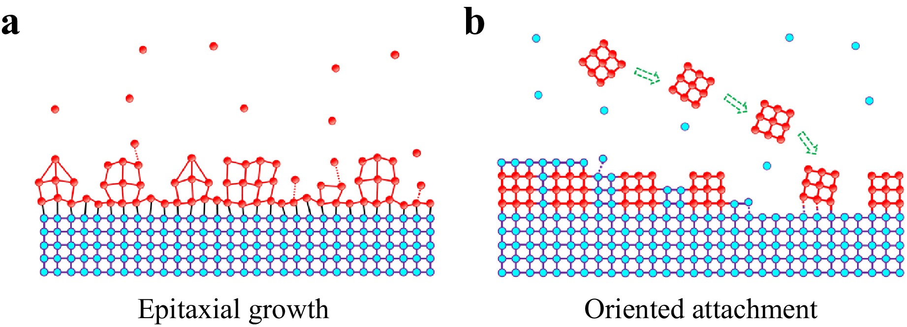
Fig. 1 Colloidal Quantum Dot-Oriented Attachment to Perovskite Single Crystal (CQD-OA-PSC) approach. a Schematical of conventional physical vacuum-based epitaxial growth, where growth takes place through atomic or molecular assembly driven by lattice-strain growth modes. b Schematic of Colloidal Quantum Dot-Oriented Attachment to Perovskite Single Crystal (CQD-OA-PSC) approach, which utilizes the precise control over quantum dot size, morphology, and structure provided by wet chemical colloidal synthesis methods, as well as the charge transport functionality imparted to the quantum dots by physical vacuum-based epitaxial growth on a matrix crystal.
-
We select PbS and CH3NH3PbBr3 to achieve quantum-dots/perovskite heterocrystals through the CQD-OA-PSC approach. These materials are chosen due to their matching cubic crystal structure and minimal lattice mismatch of only 0.2%17,18. A macroscale CH3NH3PbBr3 perovskite single crystal is prepared using a solution-phase inverse temperature crystallization method19–23. In this process, CH3NH3Br and PbBr2 (in a 1:1 ratio) are mixed and dissolved in dimethylformamide (DMF) to create a precursor solution. By maintaining this solution at 80°C for 24 hours, CH3NH3PbBr3 single crystals with sub-centimeter side length are obtained. PbS quantum dots are synthesized using PbCl2 and elemental sulfur as precursors24, with quantum dot size controlled by growth temperature and further purified through differential velocity centrifugation. As illustrated in Fig. S1, ligand exchange treatment is then performed, replacing organic oleylamine ligands with halide molecules CH3NH3Br to achieve oriented attachment25,26. Subsequently, the ligand-exchanged PbS quantum dots are dispersed in a saturated CH3NH3PbBr3 precursor solution, which is then coated onto the perovskite single crystal. This allows the quantum dots to orient themselves on the perovskite surface in alignment with its lattice, enabling controlled deposition of quantum dots layer on a macroscopic single-crystal substrate. Furthermore, this process facilitates the subsequent epitaxial growth of perovskite crystals with precisely controlled thickness following the deposition of quantum dots. This results in the formation of a double heterostructure27, characterized by enhanced electron and hole confinement within the quantum dots. Such superior confinement properties are essential in optimizing the performance of quantum dots based optoelectronic devices.
-
Fig. 2 presents transmission electron microscopy (TEM) images revealing a quantum-dot/perovskite heterocrystal. The remarkably similar lattice parameters of PbS quantum dots and CH3NH3PbBr3 perovskite necessitate the use of high-angle annular dark-field scanning transmission electron microscopy (HAADF-STEM) alongside high resolution TEM (HRTEM). HAADF-STEM provides contrast based solely on material density, independent of thickness, enabling the differentiation of PbS quantum dots. To mitigate potential electron beam-induced damage, samples are maintained at liquid nitrogen temperature using a low-temperature joystick for manipulation.
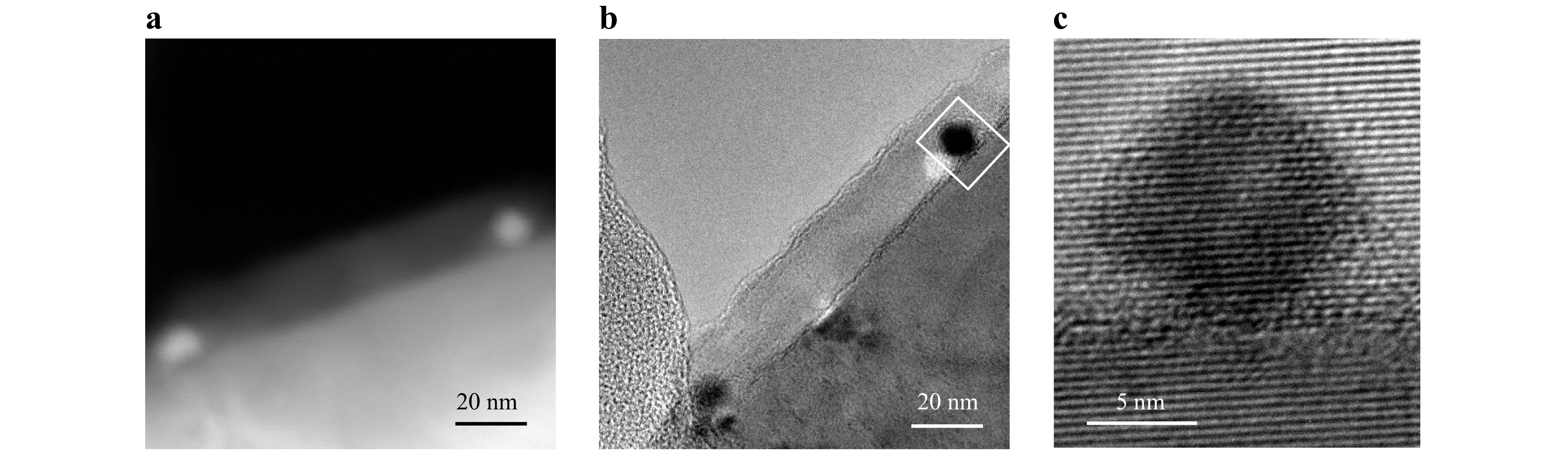
Fig. 2 Orientally attached quantum dots in ultra-thin epitaxially grown perovskite layer. a High-angle annular dark-field scanning transmission electron microscopy (HAADF-STEM) image of orientally attached PbS quantum dots in ultra-thin epitaxially grown CH3NH3PbBr3 perovskite layer, where the quantum dots are discernible as bright spots owing to their higher density. b Transmission electron microscopic (TEM) image of the same area shown in a. c High-resolution TEM image focusing on a single PbS quantum dot area, which shows that the quantum dot inherits the crystalline orientation of the CH3NH3PbBr3 perovskite substrate, sharing identical interplanar atomic spacing.
During the oriented attachment process, an ultra-thin epitaxially grown perovskite layer approximately 20 nm thick forms. In the HAADF-STEM image (Fig. 2a), PbS, with a higher density than perovskite, appears brighter, whereas in the TEM image (Fig. 2b), it appears darker. The HRTEM image in Fig. 2c focuses on a single PbS quantum dot region, illustrating its crystalline orientation inheriting that of the perovskite substrate, with identical interplanar atomic spacing. Additionally, the 20 nm perovskite layer formed during oriented attachment exhibits consistent lattice orientation and atomic spacing with both the perovskite substrate and PbS quantum dots. These observations highlight the precise alignment of the quantum dots and demonstrate the epitaxial growth's ability to fully encapsulate the quantum dots within the perovskite, resulting in a three-dimensional heterocrystal.
-
After the formation of a heterocrystal between quantum dots and single-crystal perovskite through oriental attachment, we further immerse it in a precursor solution for perovskite crystal growth. This enables the continued epitaxial growth of perovskite crystal on the quantum-dots/perovskite heterocrystal, resulting in the formation of a three-dimensional heterocrystal where quantum dots are embedded within the perovskite matrix with perfect lattice matching. As depicted in Fig. 3a, a macroscopic heterocrystal of quantum dots embedded in perovskite, exhibiting a regular rectangular shape with side lengths of approximately 7 millimeters, is obtained. Notably, the quantum dots layer enclosed within the perovskite matrix displays a darker inner square due to its higher absorbance. Fig. 3b illustrates a cross-sectional SEM image of the three-dimensional heterocrystal, showcasing a thin layer of quantum dots sandwiched between the perovskite substrate and epitaxial layer.
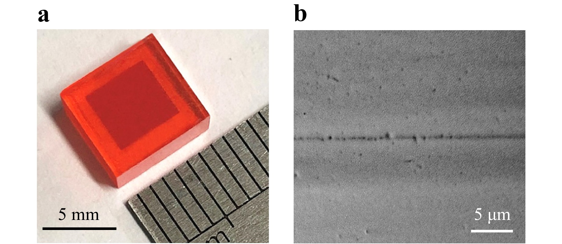
Fig. 3 Three-dimensional heterocrystal of quantum dots embedded in perovskite. a Macroscopic heterocrystal of PbS quantum dots embedded in CH3NH3PbBr3 perovskite. The quantum dots layer displays a darker inner square inside the perovskite crystal. b Cross-sectional SEM image of the three-dimensional heterocrystal. The dark line in the middle is the layer of quantum dots.
-
HRTEM is employed to conduct further investigation into the crystal structure of the three-dimensional heterocrystal composed of quantum dots embedded in a perovskite matrix. To prepare samples for HRTEM characterization, the heterostructure area is carefully scraped off onto TEM grids using a surgical blade, and images were captured under low-dose electron radiation. Fig. 4a depicts the HRTEM image of an area containing four quantum dots embedded in the perovskite matrix. Fig. 4b presents the in-situ HAADF-STEM image of the same area, where the quantum dots are discernible as bright spots owing to their higher density. Fig. 4c, e exhibit enlarged HRTEM images of areas containing pure CH3NH3PbBr3 and a single quantum dot, respectively. These atomic-resolution HRTEM images reveal that the CH3NH3PbBr3 and quantum dots within the grown heterocrystal possess perfectly matched lattice orientations. The interplanar spacings of the perovskite (0 1 1) and (1 0 1) planes, obtained from the enlarged HRTEM images, are measured to be approximately 4.19 Å and 4.20 Å, respectively, which closely match those of the quantum dot (0 1 1) and (1 0 1) planes at 4.20 Å and 4.21 Å. Fig. 4d, f illustrate the reciprocal space images obtained through fast Fourier transform for these two regions. The images reveal that the angle between the perovskite (0 1 1) and (1 0 1) planes is 60 degrees, identical to that between the quantum dot (0 1 1) and (1 0 1) planes.
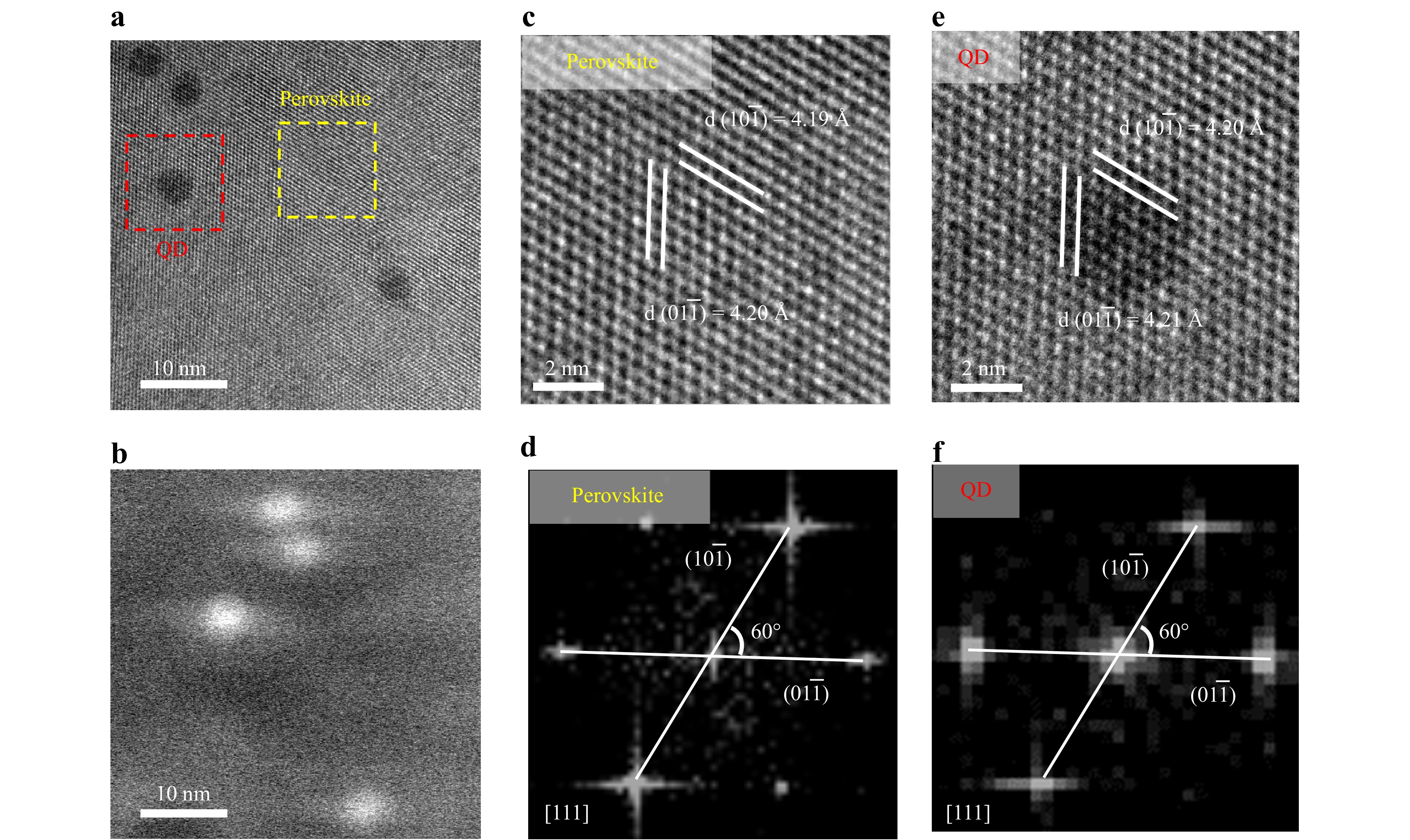
Fig. 4 High resolution transmission electron microscopic image. a HRTEM image of an area containing four PbS quantum dots embedded in the CH3NH3PbBr3 perovskite matrix. b HAADF-STEM image of the same area shown in a. c-f Enlarged HRTEM images and reciprocal space images obtained through fast Fourier transform of areas containing pure CH3NH3PbBr3 c, d and a single quantum dot e, f.
-
Tuning and ensuring the size uniformity of quantum dots is crucial for their applications in optoelectronics. However, controlling the size and uniformity of quantum dots grown via physical vacuum-based epitaxial growth methods presents significant challenges. Nevertheless, in quantum-dot/perovskite heterocrystals prepared using the CQD-OA-PSC method, the size and uniformity of quantum dots can be controlled during both the pre-oriental attachment synthesis process and the post-synthesis purification process. During synthesis, precise control over the quantum dot growth temperature allows for the manipulation of quantum dot size and uniformity. Following quantum dot synthesis, a differential velocity centrifugation method28 is employed for further purification. Fig. 5a-d depict HRTEM images and size distributions of two sizes of quantum dots with diameters of approximately 4 nm and 7 nm. The distributions indicate a relative standard deviation of less than 10% for these two sizes of quantum dots. Benefiting from their high uniformity, the photoluminescence spectra of the quantum dots with diameters of 4 nm and 7 nm exhibit very narrow full-width at half-maximum values of 130 nm and 170 nm, respectively (Fig. 5c, d). Even after synthesizing quantum dot perovskite heterocrystals using these two sizes of quantum dots, the photoluminescence spectra of the quantum dots maintain narrow linewidths similar to those of bare quantum dots. However, compared to bare quantum dots, the spectral peaks of quantum dots within heterocrystals are redshifted about 16 nm, attributable to the leakage of the quantum dots' electron wave functions into the matrix29.
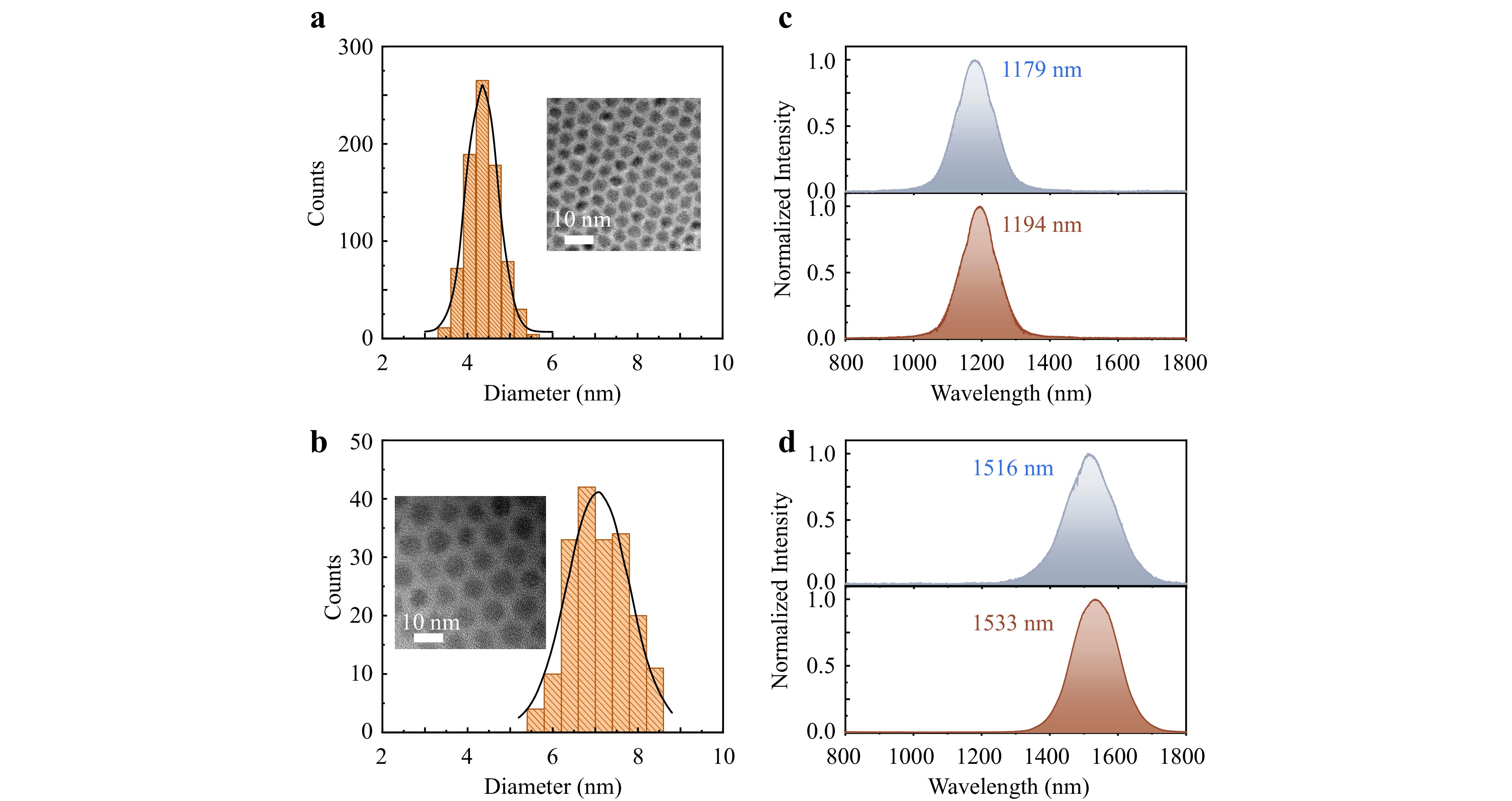
Fig. 5 Size and uniformity of quantum dots. a, b HRTEM images (insets) and size distributions of two sizes of PbS quantum dots with diameters of approximately 4 nm a and 7 nm b. c Photoluminescence spectra of the quantum dots with diameters of approximately 4 nm. Top: Bare quantum dots. Bottom: quantum dots within heterocrystal. d Photoluminescence spectra of the quantum dots with diameters of approximately 7 nm. Top: Bare quantum dots. Bottom: quantum dots within heterocrystal.
Fig. S2 show the UV-Vis and photoluminescence (PL) characterization of the samples. For the bare perovskite sample, the absorption increases dramatically around its band edge, approximately 550 nm. For the PbS quantum-dot/perovskite heterocrystals sample, there is an additional absorption peak around 1200 nm, corresponding to the absorption of PbS quantum dots (Fig. S2a). To characterize the charge transfer from perovskite to PbS quantum dots, we obtained PL images in the cross-sectional area of the quantum-dot/perovskite heterocrystals using a 488 nm laser as the excitation source (Fig. S2b). The images were collected by near infrared (NIR) and visible cameras, respectively. In the image captured by the NIR camera, PL from the quantum-dot layer is clearly visible. In the image captured by the visible camera, the perovskite layers surrounding the PbS quantum dots emit strong green PL, while the middle perovskite layer, containing only 8% quantum dots, is distinctly quenched. These observations indicate effective charge transfer from the perovskite to the PbS quantum dots in the heterostructure11,12.
The double heterostructure in the quantum-dot/perovskite heterocrystal ensures strong electron and hole confinement within the quantum dots, and the perfect lattice matching eliminates detrimental interface trap states. This results in improved carrier recombination efficiency and enhanced PL emission intensity in the heterocrystal. As shown in Fig. S2c, the emission intensity of the quantum dots more than doubles after being integrated into the perovskite as a quantum-dot/perovskite heterocrystal, compared to their emission in the colloidal state at the same concentration.
-
Synthesis of CH3NH3Br: The synthesis of CH3NH3Br involves the blending of HBr and a CH3NH2 solution in a molar ratio of 1.5:1, followed by stirring in an ice-water bath for 2 hours. The resulting mixture is then subjected to reduced pressure distillation for crystallization, and further purified through recrystallization using diethyl ether. Subsequently, it is dried under vacuum conditions and stored in an N2 atmosphere.
Growth of CH3NH3PbBr3 single crystals: The growth of CH3NH3PbBr3 single crystals involves the mixing and dissolution of CH3NH3Br and PbBr2 (in a 1:1 ratio) in dimethylformamide (DMF) to form a precursor solution. Sub-centimeter-sized CH3NH3PbBr3 single crystals are grown by maintaining the precursor solution at 80 °C for 24 hours.
Synthesis and purification of PbS quantum dots: We first prepare a solution comprising 0.08 g of sulfur dissolved in 7.5 mL of Oleylamine by heating the mixture under nitrogen for 30 minutes at 120 °C. Subsequently, a blend of 0.834 g PbCl2 and 7.5 mL Oleylamine is introduced into a three-neck flask, and subjected to degassing for 30 minutes under nitrogen at 125 °C. The PbCl2 solution is then adjusted to the necessary injection temperature, and 2.25 mL of the Oleylamine-S stock solution, accompanied by 170 μL of tri-n-octylphosphine, is swiftly injected. This injection typically results in a temperature decrease of approximately 5−10 °C, with the ensuing growth temperature meticulously maintained throughout the reaction duration. Upon reaching the desired growth period, the reaction is promptly quenched by the addition of 10 mL of toluene and 15 mL of ethanol. The solution undergoes centrifugation to precipitate excess PbCl2, with the supernatant carefully transferred to a separate test tube. Following further centrifugation and supernatant removal, the quantum dots are re-suspended in 10 mL of toluene. The quantum dot size control is achieved by adjusting growth temperatures spanning from 80 to 160 °C. Post-synthesis, differential velocity centrifugation is employed to enhance quantum dot purity. This purification process involves resuspending the purified quantum dots in toluene, followed by ethanol precipitation to eliminate residual impurities. As the method of differential velocity centrifugation, we add 10% v/v ethanol to the quantum dots solution with toluene as the solvent, then centrifugal at 3000 rpm for 10 min, collect precipitated quantum-dots and transfer the supernatant to centrifugal at 5000 rpm for 10 min. Then, collect precipitated quantum-dots again and transfer the supernatant to centrifugal at 6000 rpm for 10 min. In turn like this, centrifugal at 7000 rpm, centrifugal at 9000 rpm. The separately collected precipitated quantum-dots will have the narrower size distribution than the initial solution. The result of the differential velocity centrifugation is a quantum dots population exhibiting a notably more uniform size distribution. Ultimately, the purified quantum dots are suspended in toluene and meticulously stored under nitrogen, shielded from light exposure.
Growth of quantum-dot/perovskite heterocrystals: The PbS quantum dots synthesized are coated with long organic chains of Oleylamine to prevent nanoparticle aggregation. However, these extended ligands pose a challenge by limiting their solubility in polar solvents like DMF and impeding their oriented attachment to perovskite. Therefore, a ligand exchange treatment becomes imperative. Solution-based ligand exchange is executed by blending PbS quantum dots in an octane solution with a DMF solution containing CH3NH3PbBr3 perovskite precursors (PbBr2 and CH3NH3Br, in a 1:1 ratio). After a brief stirring period of 10 minutes, efficient ligand exchange is evidenced by the migration of quantum dots from the upper octane phase to the lower DMF phase. This indicates successful replacement of the original Oleylamine ligands on the PbS quantum dots surface with halide molecules of CH3NH3Br. Following octane removal, the quantum dots solution undergoes three additional washes with octane to eliminate any residual organic matter. Subsequently, the quantum dots are precipitated by adding toluene. The nanoparticles are then dispersed in a saturated CH3NH3PbBr3 precursor solution. Subsequently, 4 μL of the quantum dots solution is dispensed onto the perovskite substrate, and let it dry naturally, allowing the quantum dots to orient themselves on the perovskite surface in alignment with its lattice. The subsequent epitaxial growth of perovskite crystals is realized by immersing quantum-dot/perovskite heterocrystals in the perovskite precursor solution.
-
SEM characterization: Cross-sectional samples are crafted using a ThermoFisher Helios G4 UX system employing focused ion beam etching (FIB). Subsequently, scanning electron microscope (SEM) images are acquired utilizing a ThermoFisher Helios G4 UX electron microscope, employing a consistent operating condition with an accelerating voltage of 5 kV and a beam current of 87 pA across all samples.
Transmission electron microscopy characterization: HRTEM characterization samples are obtained by scraping off the heterojunction area onto lacy carbon TEM grids using surgical blades. It’s noteworthy that organic–inorganic hybrid perovskites are highly susceptible to electron-beam irradiation and prone to decomposing into PbX2 under TEM characterization30. All HRTEM and HAADF-STEM images were captured using a Titan Cubed Themis G2 300 microscope (K2+OneView camera) operating at 300 kV, with an electron dose of 15 eÅ−2 s−1 during experiments. To minimize potential damage to the quantum-dot/perovskite heterocrystals caused by the electron beam, samples are placed at liquid nitrogen temperature using a low-temperature joystick for measurement, omitting the process of finding the zone axis. Prior to imaging, TEM parameters were meticulously adjusted near the sample, enabling the swift movement of the electron beam to the sample position to capture HRTEM images promptly. Upon acquiring an available HRTEM image, the imaging mode is swiftly switched to HAADF to capture the in-situ HAADF-STEM image.
Optical measurements: The photoluminescence spectra of both quantum dots and quantum-dot/perovskite heterocrystals are captured at room temperature using a 633 nm femtosecond laser as the excitation source, with a pulse length of 150 fs and a repetition rate of 6 kHz. A custom-built microscopy system, featuring a near-infrared CCD and spectrometer, facilitates the characterization of the emission properties. This system is equipped with a shared objective lens (50×, NA = 0.42) to collect both excitation and emission beams.
-
In summary, we have presented a novel approach for the growth of quantum-dots based heterocrystals termed Colloidal Quantum Dot-Oriented Attachment to Perovskite Single Crystals (CQD-OA-PSC). The CQD-OA-PSC method involves the growth and optimization of quantum dots through chemical colloidal synthesis methods, followed by their oriented attachment onto the surface of macroscopic perovskite single crystals. This results in the formation of high-quality heterocrystals characterized by perfect lattice matching. The CQD-OA-PSC method synergizes the advantages of two distinct quantum dot synthesis approaches: wet chemical colloidal synthesis method and the physical vacuum-based epitaxial growth method. It harnesses the precise control over quantum dot size, morphology, and structure offered by wet chemical colloidal synthesis method, while also leveraging the charge transport functionality conferred to the quantum dots by the matrix crystal in physical vacuum-based epitaxial growth method. Confirmation of matched lattice orientations between the perovskite matrix and quantum dots is achieved through high-resolution transmission electron microscopy. The CQD-OA-PSC approach represents a promising method for synthesizing high-quality quantum-dots/perovskite heterocrystals with controlled size, morphology, and optoelectronic properties. This advancement holds significant promise for the development of efficient optoelectronic devices, including light-emitting diodes, solar cells, photodetectors and lasers.
-
This work is supported by National Natural Science Foundation of China (grant nos. 12225402, 91950115, 11774014, 62321004), national Key R&D Program of China (grant nos. 2022YFA1404700, 2018YFA0704401) and the New Cornerstone Science Foundation through the XPLORER PRIZE.
Colloidal quantum dots on macroscale perovskite single crystal with perfect lattice matching
-
Yu-Hao Deng1, 2, 3,
 ,
, - Yun-Gang Sang1, 2, 4,
- Xiao-Wei Zhang1, 2, 5,
- Yi-Fei Mao1, 2, 6,
-
Ren-Min Ma1, 2, *, ,
- Light: Advanced Manufacturing 6, Article number: 9 (2025)
- Received: 27 March 2024
- Revised: 04 December 2024
- Accepted: 04 December 2024 Published online: 07 March 2025
doi: https://doi.org/10.37188/lam.2025.009
Abstract: Quantum dots, semiconductor crystals with nanometer-scale dimensions, exhibit adjustable chemical, electrical, and optical characteristics owing to the quantum confinement effect. However, achieving high-quality quantum dots necessitates simultaneous attainment of crystalline integrity within their cores, uniformity in size and shape, as well as effective surface passivation with charge transport functionality—challenges persist regardless of the chosen method. Here, we introduce a novel approach for synthesizing quantum-dot/perovskite heterocrystals: the Colloidal Quantum Dot-Oriented Attachment to Perovskite Single Crystal (CQD-OA-PSC) method. This method involves optimizing quantum dot growth through chemical colloidal synthesis methods, followed by their oriented attachment onto macroscopic perovskite single crystals with impeccable lattice alignment. Consequently, the CQD-OA-PSC method amalgamates the strengths of wet chemical colloidal synthesis methods and solution-based epitaxial growth, offering precise control over quantum dot size, morphology, and structure while leveraging charge transport functionality conferred by the matrix crystal. High-resolution transmission electron microscopy confirms matched lattice orientations between the perovskite matrix and quantum dots. This approach promises to yield high-quality quantum dots perovskite heterocrystals with controlled size, morphology, and optoelectronic properties, thereby holding significant potential for advancing the development of efficient optoelectronic devices.
Rights and permissions
Open Access This article is licensed under a Creative Commons Attribution 4.0 International License, which permits use, sharing, adaptation, distribution and reproduction in any medium or format, as long as you give appropriate credit to the original author(s) and the source, provide a link to the Creative Commons license, and indicate if changes were made. The images or other third party material in this article are included in the article′s Creative Commons license, unless indicated otherwise in a credit line to the material. If material is not included in the article′s Creative Commons license and your intended use is not permitted by statutory regulation or exceeds the permitted use, you will need to obtain permission directly from the copyright holder. To view a copy of this license, visit http://creativecommons.org/licenses/by/4.0/.

 DownLoad: