


-
PIC technology not only powers the modern internet, but is also widely acknowledged as a game-changing technology that promotes a host of innovations, including integrated quantum processing units1,2, artificial intelligence accelerators3,4, and light-based detection5 and ranging imaging systems6, etc. Arguably, the two most prominent integration platforms that have been widely commercialized are indium phosphide (InP) and silicon-on-insulator (SOI)7,8. The former offers light sources and amplifiers with good electro-optic performance, while the latter offers high-volume manufacturing capacity and high light confinement. One approach to combine the light emitting/amplifying capability of InP with the full scalability of SOI, advanced integration schemes, spanning flip-chip bonding9, die/wafer bonding10, micro-transfer printing11, and direct epitaxial growth12, have been heavily researched. Alternatively, to harness the potential of photonic integration platforms to meet the ever-increasing circuit-level performance metrics, such as low waveguide propagation loss13, high electro-optic coefficient14, high Kerr coefficient15, and second-order nonlinearity, etc., a range of different waveguide materials, such as silicon nitride15, lithium niobate10, gallium nitride16, and aluminum nitride, have all been investigated. Foreseeably, to break the limitations of a single material platform, hybrid and heterogeneous integrations that create different cross-platform systems will continue to play a critical role. Indeed, recent demonstrations on III-V gain materials co-integrated on thin-film lithium niobate and silicon nitride17 have opened new opportunities for high-performance chip-scale optical systems.
Notable demonstrations on cross-platform integrations are summarized in Supplementary 1. The most distinctive property of each material for integration is probably its refractive index as it defines the achievable refractive index contrast to form a waveguide and hence the achievable waveguide mode diameter. Therefore, different integration technologies often come with different material interfacing methods, ranging from grating coupling, butt coupling, adiabatic coupling, to evanescent coupling. The primary considerations are generally low inter-waveguide coupling loss, high fabrication tolerance, and wide operation bandwidth18. The resulting required alignment tolerance is often regarded as key for scalable production capacity19. Direct epitaxial growth of III/V materials onto the SOI platform may represent the ultimate path but currently has a low technology readiness level. Die/wafer bonding and micro-transfer printing are promising paths but require dedicated processing steps. Flip-chip bonding is a process generally performed after each die is fabricated on its own technology platform. A standard but additional process is required, i.e., back-end opening and metallization, to allow die placement and bonding.
Photonic wire bonding (PWB) stands out as an assembly technology for multi-platform photonic interconnection with great potential. It only requires coarsely pre-positioned photonic dies with the assistance of a 3D machine vision technique boasting sub-100 nm precision. Yet, additional post-processing steps, such as back-end opening, are imperative to expose the waveguide from the cladding layer. It is also noteworthy that the printed optical wires leave relatively substantial footprints, measuring at least sub-hundred micrometers without on-chip parts, as a prerequisite for achieving reasonable adiabatic coupling efficiency. The nature of this linear processing route inherently results in a time-consuming procedure. A comprehensive review of 3D-printed optical couplers is also included in Supplementary 1.
In this manuscript, we present an alternative strategy for facilitating photonic chiplet interconnection via a novel 3D-nanoprinted interposer. The proposed optical interposer incorporates a substrate that accommodates 3D-nanoprinted elements responsible for establishing optical interconnections among dies of different material platforms and optical fibers. A conceptual hybrid chiplet integration is illustrated in Fig. 1a, elucidating the spatial configuration of diverse 3D-printed components, including parabolic reflectors, mechanical supports, fiber funnels, and chip fixers. Its compact couplers that also handle arbitrary mode size conversion pave the way for high-density hybrid chiplet integration using 3D-nanoprinting (Fig. 1b). The offset between the input and output optical axis can be utilized for height difference compensation by rotating the coupler (Fig. 1c). By coordinating mechanical and optical structures, this co-design method ensures minimum requirement on chip alignment both spatially and angularly. Thus, it represents a generic solution that can readily couple between chips fabricated in material systems with zero change in their individual process flows.
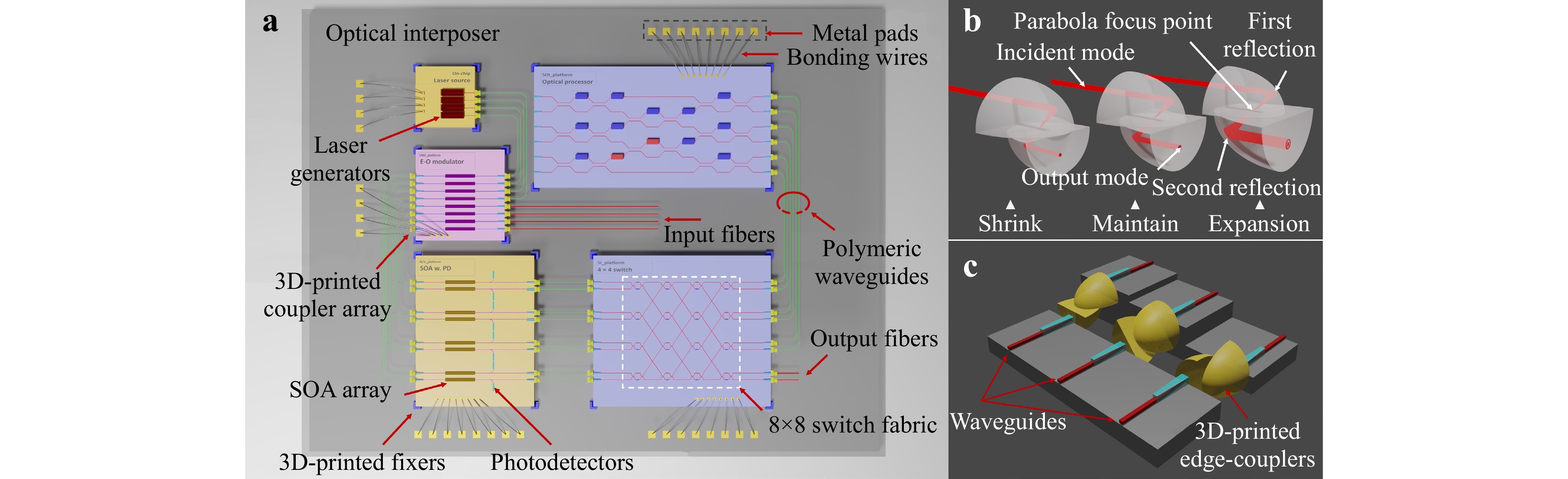
Fig. 1 a Conceptual schematic of chiplet interconnection realized by 3D printing. Notable components include on-chip laser generators and a semiconductor optical amplifier (SOA) array produced using a III/V platform, an electro-optic modulator chip fabricated with an LNO platform, and an optical processor and switch device from an SOI platform. The chiplets, originating from different optical platforms, are fixed by clamps onto an interposer. Mode size converters and aligning funnels are printed between different chips and fibers. b Schematic of the parabolic-shaped edge coupler. The incident beam propagates within the TPP resin structure and reflects at the resin/air interface. Based on the geometrical design of the edge coupler, the input Mode Field Diameter (MFD) can be maintained or expanded, and aberrations can be corrected by adjusting the relative positions of the two reflectors. c Inter-chip couplers with arbitrary rotation angle. The couplers are directional-insensitive, such that they can be arranged to have a certain angle to help compensate height differences between adjacent chips.
We here demonstrate a micron-scale optical interposer that efficiently connects silicon and InP chips, with standard optical single-mode fibers (SMFs) as input/output connections. The arrangement of a simple two-chip integration is illustrated in Fig. 2a, with close-ups of the fiber-to-chip and chip-to-chip coupling units plotted in Fig. 2b, c. This innovative photonic chiplet interconnection archives ultra-wide bandwidth, a substantial mode conversion ratio, and passive alignment capability.
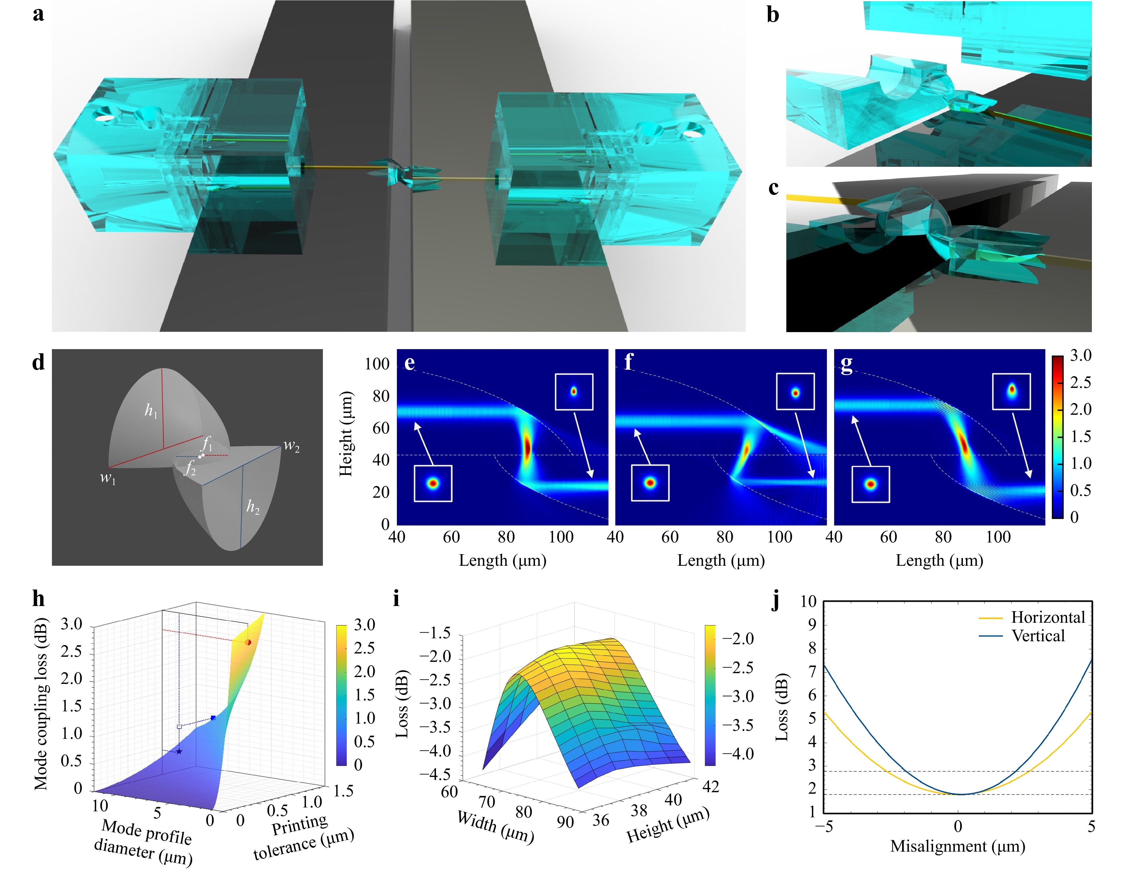
Fig. 2 a 3D rendering of a chip-to-chip testing sample. Three pairs of parabolic-shaped reflectors are placed at the input/output and inter-chip for fiber-to-chip and chip-to-chip coupling, respectively. The funnel-like structure on top of the chips is to accommodate optical fibers. Bayonet-shaped mechanical support is added to improve the stability. Close-up of b the fiber-to-chip coupling unit, and c the chip-to-chip coupling unit. d Schematic of a coupling unit consisting of a pair of parabolic-shaped reflectors, with key parameters highlighted. Light propagation paths simulated with Lumerical FDTD module at different laser injecting positions having e a balanced leakage and aberration, f too much leakage, and g too much aberration loss. h 3D plot of the mode coupling loss introduced by limited printing accuracy at different MFDs. The red solid dot and the blue star marks the targeted coupling loss for 4 μm and 10.4 μm MFD coupling, with 1μm printing accuracy, respectively. i Mesh plot of the geometry optimization result from Lumerical FDTD simulations. j Parameter sweep results from the Lumerical FDTD simulation for the misalignment tolerance evaluation in horizontal (yellow) and vertical (blue) directions acquired at a wavelength of 1550 nm. The 1 dB-loss window is marked with the dashed lines. The simulation is carried out on a quasi-10 µm to 4 µm MFD conversion.
-
The mode size converter employs a pair of parabolic-shaped reflectors. The incident light turns into a convergent beam after the first reflection at the resin/air interfaces, and travels through the focal point. The key of having a pair of parabolic-shaped reflectors is that, when they share the same focal point, the output beam turns back to a collimated beam that can be easily coupled to a waveguide. Furthermore, it enables efficient conversion of the mode field diameter (MFD), as detailed in the following subsection. The geometry of the parabola is tailored to precisely manipulate the light propagation. As illustrated in Fig. 2d, the key parameters include the widths w1, w2, heights h1, h2, and the focal lengths f1, f2, of the two parabolic-shaped reflectors.
-
When the pair of parabolic reflectors are symmetrical (f1 = f2), the input MFD will remain unchanged at the output. Changing the second reflector’s dimensions alters the MFD of the output mode, achieving effective mode size conversion at low loss, as shown in Fig. 1b. Due to the free-space propagating nature of light inside the coupler and its 3D designing freedom, compact but ultra-wide bandwidth coupling can be achieved.
Considering a monochromatic, highly collimated incident laser beam, the output mode will have a new MFD d2 of d1*f2/f1, where d is the MFD of the input mode, f1 and f2 being the focal length of the first and second parabola, respectively. Thereafter, we can denote the MFD conversion ratio φ, as φ = f1/f2. Lumerical FDTD (finite difference time domain) software is subsequently used to visualize the light propagating inside the reflectors input from a guided mode and enables optimization of the design. An example is as follows: Fig. 2e shows a side view of the optical propagation path at the wavelength of 1550 nm, and the parameters of the two parabolic-shaped reflectors are set differently to shrink the output mode. However, due to the polychromatic nature of the laser beams and the spherical aberration introduced by the reflections happened at the concave polymer/air interfaces, the geometry of reflectors needs to be tailored to optimize coupling efficiency (Fig. 2f) and correct comatic aberration (Fig. 2g). The focus point is not located at the interface of the two parts, and this is mainly because the input mode lose constrains from the core/cladding interface after it leaves the optical waveguide and becomes a divergent beam. The actual focal points of the reflectors are tweaked with the assistance of FDTD modeling. For the actual test, limited by the tool’s alignment capability, the coupling loss will be slightly higher than the designed value, which is explained in Fig. 2h. A more detailed description of the mode adaptation can be found in Supplementary 2.
-
The geometry of the parabola is first calculated using linear optics to provide an initial design with the target mode conversion ratio, taking the beam divergence into consideration. For the case of a Gaussian beam emitted at the end of the optic fiber that enters the reflecting units, according to ISO 11146-1:200518, the divergence half-angle, θ, is calculated from Eq. 1:
$$ \theta =\frac{\lambda }{\pi n{w}_{0}} $$ (1) where λ is the wavelength of the light source, n is the refractive index of the resin that is used to shape the reflectors, and w0 is the waist size. For the case of an integrated waveguide, similar estimations can be made.
Here, considering a laser beam that has a center wavelength of 1550 nm emitting from an SMF28 optical fiber that has an MFD of 10.4 µm, the divergence half-angle is calculated to be around 4°. Since the wavefront of the incident light is not planar, not all incident light is parallel to the main optical axis of the parabolic reflector. Therefore, comatic aberration occurs at the output. Also, the output mode will be expanded slightly due to the beam divergence. The incident angle at the output part then defines the output mode size, which can be described as:
$$ {MFD}_{out}= 2\left[\mathrm{arctan}\left(\frac{{y}_{1}+t}{2x}\right)+\mathrm{arctan}\left(\frac{{y}_{2}+t}{2x}\right)\right] $$ (2) where y1 and y2 denote the upper and lower boundary in the vertical direction, t denotes the incident height and x denotes the width of the parabola.
We simulate a pair of reflectors with Rhinocero for a proof-of-principle scenario with an SMF28 as input and an integrated waveguide of a 4 μm MFD as output. The 3D model files are imported into Lumerical to conduct FDTD simulations. The input mode is set to have a central wavelength of 1550 nm, and the parameter sweep results of the reflector geometry are plotted in Fig. 2i.
-
The reflectors are designed in such a way that they transmit the input with a low loss and with a high misalignment tolerance (Fig. 2i, j). However, even though the condition for total internal reflection (TIR) is met, comatic aberration still occurs due to the beam divergency of the incident laser, which is a major source to the signal loss as it results in some mode mismatch. To minimize the comatic aberration, a lower incident point is preferred for the input mode as shown in Fig. 2f. However, this will in turn increase the loss due to light leakage as a result of the beam divergence during the free-space propagation within the reflectors that leads to a reduced incident angle at the resin/air interface. Therefore, a careful trade-off has to be made. The best incident spot and reflector geometry are identified using Lumerical FDTD with perfectly matched layer (PML) boundary conditions. The simulation result shows that 20 μm from the top of the parabola is the best position to balance light leakage and aberration. As a result of optimization via simulations, the mode size conversion loss can be minimized at around 0.7 dB, presumably bounded by the beam divergence. This could be further optimized by the use of irregularly shaped reflectors but this would compromise its ease of fabrication. The width and height of the reflector are optimized to be 82 μm and 38 μm, respectively, in this design example.
-
Alignment tolerance is evaluated using Lumerical FDTD. The tolerance in both vertical and horizontal directions is greatly improved compared to the loss level without the parabolic reflectors. The 1 dB-loss window is increased from about 1 μm to about 6 μm in the horizontal direction and to about 4 μm in the vertical direction, as shown in Fig. 2j. Additional information can be found in S2 of Supplementary.
To sustain a low coupling loss, it is required to keep both the input and output interfaces well aligned. We introduce a smart on-interposer coupling frame, composed of fixers and gripping clamps, as detailed in the following subsection, that is pre-printed to fix the position of the various dies. Subsequently, on-chip funnels are printed to ensure an accurate alignment of fibers. The coupling funnel’s geometry is designed as 500 × 300 × 300 μm, truncated by a circular cone with a lower diameter of 130 μm and an upper diameter of 250 μm, taking resin shrinkage into consideration. The model of the frame intrudes into the chip edge by 20 μm, such that a tight fit between the resin frame and the chip edge is guaranteed after the printing process, and a sub-micrometer alignment accuracy can be achieved. A bayonet of 20 μm is presented at the end of the truncated cone to enhance the plug-in process’s stability, as shown in Fig. 2b.
-
The optical chiplet interposer concept is designed to leverage 3D-nanoprinted fixers to align chiplets and flexible clamps to provide additional grip force. Fig. 3 schematically describes the solution. The fixers are printed at the four corners where the chiplet will be placed, and the upper edges of the fixers are chamfered to allow the chip to be placed easily. A layer of resin under the fixer can be used to compensate for the height difference between different chiplets. The fixers enable a positioning accuracy of ±1 µm, and in order to push towards sub-micrometer accuracies, mechanical clamps are introduced, which are printed at opposite sides of a chiplet (demonstrated in Silicon-InP die-level interconnection). Besides, the fixers also help to ensure a smaller angular deviation between their respective axes of the chiplets, which eases the following on-chip printing aligning process. The crimps in the clamps that are pushed outwards by the chiplet provide a restoring force, which helps fix the chiplets in position and provides relative coordinates to help quickly locate and identify the markers for the following on-chip printing processes.
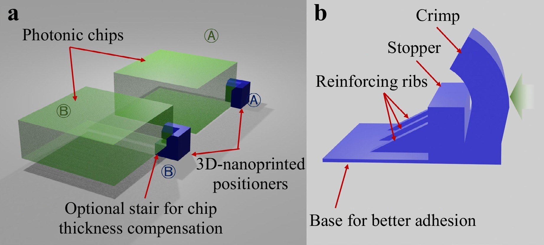
Fig. 3 Schematic of the 3D-nanoprinted chiplet fixing solution. a Fixers that can help compensate height differences, and b clamper for additional gripping force.
-
The fabrication was carried out using a commercial direct laser writing system (Nanoscribe Professional GT2) with a printing setup consisting of a 25× objective and IP-n162 and IP-S resin provided by Nanoscribe. The refractive indices of these two resins are around 1.6 and 1.49 respectively. This choice of resin and objective is to ensure fast fabrication while maintaining good resolution. First, chip clamps and fixers are fabricated onto ITO (indium tin oxide) coated silica substrate (which is aimed for easier printing interface finding) to form the framework of the chiplet interposer. The chip clamps and fixers play a vital role in offering preliminary alignment. Then, dies of different materials are placed into the coupling frame formed by the clamps and fixers. After the chips are settled, the coupling funnels and parabolic mode size converters are fabricated onto the chips using one-step printing to ensure good alignment. The most critical step is the pre-printing alignment, which needs to be verified both vertically and horizontally. The relative coordinates between the chip edge and couplers offer a reference, whilst a finer adjustment is done horizontally with the assistance of the visual monitoring system in Nanoscribe GT2. As for the vertical aspect, we use the interface of the ITO-coated substrate and the base layer as a reference, taking advantage of their high refractive index contrast. The printing process utilizes a smaller laser power and slower scanning speed for the optical part to minimize surface scattering and a higher laser power and faster scanning speed for the mechanical part to reduce the printing time. The entire printing process takes approximately 25 minutes. After laser writing, the polymerized structure is developed in propylene glycol monomethyl ether acetate (PGMEA) for 15 minutes to remove unexposed resin, and in isopropanol (IPA) for 5 minutes to remove excess PGMEA. The device is then subjected to UV curing for improved mechanical stability.
-
In practice, the largest mode mismatch occurs for off-chip coupling where light couples from a standard single-mode fiber to a chip. As a result of the high index contrast of the silicon-on-insulator platform, the MFD in the tapered edge coupler of the chip is about 5 × 7 μm2 which is fixed by the foundry’s standard working flow. By optimizing the geometry of the coupler, our design can convert symmetrical modes into asymmetrical ones, or in other way round. As a result, couplers with a mode diameter converting ratio as large as 2:1 are required as the MFD of SMF28 is about 10.4 μm, at a wavelength of 1550 nm. To evaluate the coupling and the MFD conversion loss, we use test couplers between optical fibers with different numerical apertures (Fig. 4a, b). The input mode has an MFD of 10.4 μm from SMF28, and the receiving optical fiber is selected to be either an SMF28 at a conversion ratio of 1:1, an HNA fiber that has an MFD of 6.8 μm and a conversion ratio of 3:2, or a UHNA fiber that has an MFD of 4.7 μm and a conversion ratio of 11:5. A coupler consisting of two pairs of reflectors is also developed for evaluating its cascading capability (Fig. 4c) for higher conversion ratios. The excess coupling loss is, however, higher than expected due to the doubled non-constrained propagation of the divergent beam. For all testing, cleaved fibers are used. The fabricated prototypes are first attached to a 3-axis optical stage (Thorlabs MAX312D), and then characterized by a tunable laser (Keysight 81609A) sweeping from 1480 nm to 1620 nm.
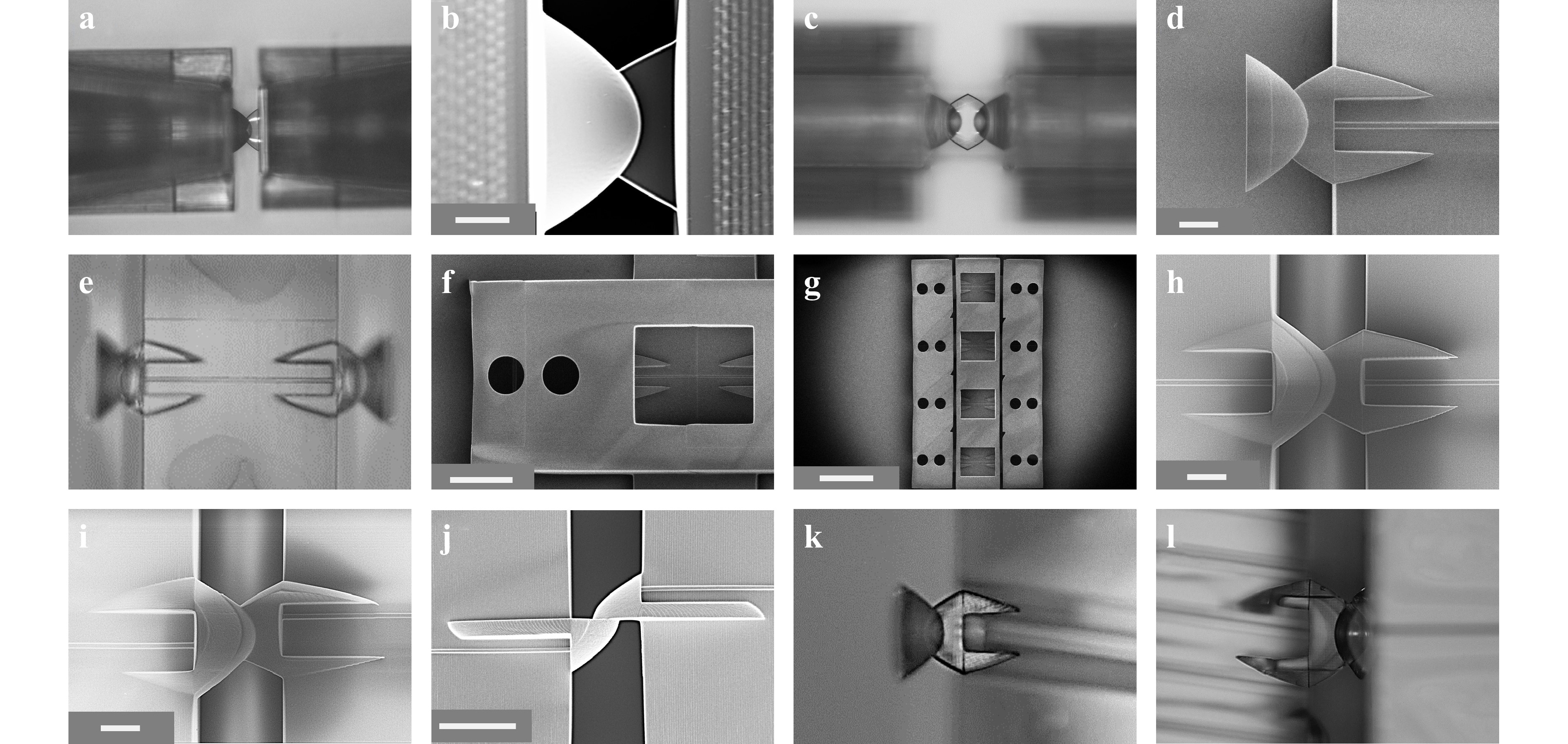
Fig. 4 a Microscope image of a fiber-to-fiber testing sample with two funnels at each side of the reflectors (scale bar 100 μm), and b SEM close-up of the reflectors, scale bar 20 μm. c Microscope image of a dual-pair reflectors for cascading validation, scale bar 100 μm. d SEM image of reflectors printed on a full-polymeric chip, scale bar 20 μm. e Microscope image (scale bar, 50 μm) of a fiber-to-chip test sample. f SEM image of the sample in, with the funnel structure added (scale bar, 60 μm). g SEM image of a four-channel fiber-to-chip test sample scale bar 300 μm. Close-up SEM image of chip-to-chip couplers with a rotation angle of h 0°, i 30° (h, i, scale bar 20 µm), and j 90° (scale bar, 40 µm). k Microscope image of an angled coupler (scale bar, 40 μm). l Microscope of an angled chip-to-chip coupler (scale bar, 40 μm).
-
The fiber-to-chip coupling loss is evaluated by comparing the coupling efficiency with and without the coupler. The mechanical clamping unit is implemented for both cases to remove the effect of the alignment funnel on fibers. To better control variates, an in-house printed polymer chip using the IP-series resins with integrated waveguide is developed and used for a set of tests that help gain fresh insights into the tailoring of the coupling unit. A walkthrough of the sample chip preparation method is depicted in Supplementary 5. Fig. 4d−f shows the printed test structures. The MFD of the polymer waveguide is designed to be around 4 μm which is close to that of the edge coupler in a foundry-produced Si chip. The parabolic-shaped couplers are printed on the polymer chip following the processes outlined in Fabrication process, to couple light into and out of the chip from the standard SMF28, and this corresponds to a mode size mismatch of 84% difference in size. According to the Lumerical FDTD simulation, there is a theoretical loss of 1.7 dB/facet between the SMF28 and the chip, mainly coming from the mode mismatch. Experimentally, an input/output (I/O) loss of 2.4 dB/facet is measured over a wide range of wavelengths from 1480 nm to 1620 nm (see Fig. 5a). Compared to the simulated coupling loss, the measurement result shows a total excess I/O-loss of 0.7 dB/facet that comes from the variations in the chip dimensions, surface roughness of the printed structures, reflections at the polymer/air and polymer/waveguide interfaces.
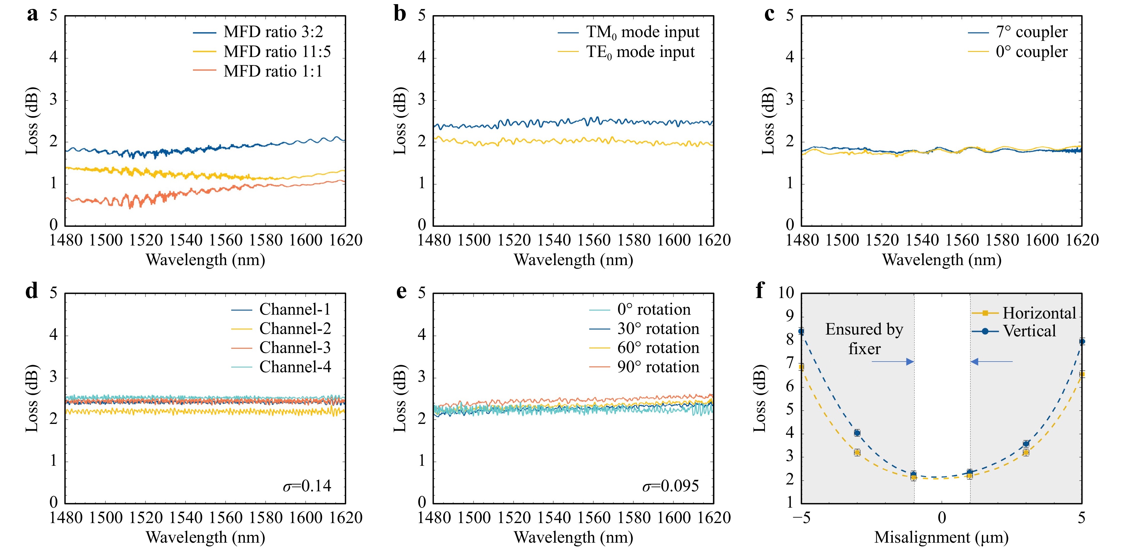
Fig. 5 a MFD conversion test with ratios of 1:1, 3:2 and 11:5. Measured coupling efficiency of b TE0 and TM0 modes, and c 7°-anti-reflection angled coupler. d Multi-channel fiber-to-chip coupling efficiency test. e Chip-to-chip coupling efficiency with the coupler rotated at an angle of 0°, 30°, 60°, and 90°. f Misalignment tolerance evaluation. A sub-micrometer accuracy can be achieved with the help of the funnel structure. All the couplings are conducted from SMF28 to polymer waveguides with MFDs of 4 × 4 µm2.
For photonic integrated devices, it is often desirable to achieve good coupling efficiency for both transverse electric (TE) and transverse magnetic (TM) modes. The fabricated coupler is thus also characterized using a polarimeter (Thorlabs PAX1000). The measurement results are plotted in Fig. 5b. It is noticed that the TM0 mode has a slightly higher loss than the TE0 mode. This is mainly caused by the smaller effective index of the TM0 mode, which will result in more leakage at the polymer-air interface. Besides, for the purpose of reducing reflection at the interface, a small tilted angle is usually introduced to the edge coupler. We tested both cases, with and without an anti-reflective angle of 7°. The measurement result is plotted in Fig. 5c, and it shows that the coupler design has good compatibility with the angled edge couplers. Additionally, a common strategy to increase the optical I/O throughput is to have arrayed couplers. Thanks to the small footprint of the parabolic-shaped coupler, it is simple to have an array of couplers 3D-printed on-chip, as illustrated by Fig. 4g. For now, the pitch is set at 300 µm, which is limited by the current funnel size. However, the pitch can be easily reduced as the adjacent funnels can be partly merged, without any compromise to mechanical stability. By optimizing the recipes, it is possible to reduce the pitch to 127 µm, a common standard used in photonic I/Os. Loss measurements for the four-channel prototype are shown in Fig. 5d, with the loss consistent in all four channels.
-
Similarly, polymeric chips that contain integrated waveguides are fabricated and used to emulate die-to-die interconnections between chiplets. The waveguides on the first and second chips are designed to have MFDs of 4 μm and 2 μm, respectively, in order to emulate typical MFDs of InP and Si waveguides. According to a Lumerical FDTD simulation, the coupling loss between the chips is 1.6 dB20. with couplers attached In the experiment, the chip-to-chip coupling loss is measured to be <2.5 dB, in which the excessive loss is believed to arise from the surface roughness but also the misalignment that is induced by the fabrication itself. The in-plane alignment of the chips is secured by the pre-printed clamps on the interposer. As photonic chips from different platforms often have different heights, it is necessary to compensate for the height difference whilst mode coupling. One of the advantages of the coupling unit is that, it can be rotated to help compensate for the height difference. In the experiment, the coupling unit is rotated 30°, 60° and 90° respectively, SEM images shown in Fig. 4h−j. According to the tests, the coupling loss remains comparable with different rotation angles, with a loss of 2.3 dB (Fig. 5e), which proves the ability of the device to solve the vertical alignment in chip-level coupling (Fig. 5f).
-
Finally, the developed designs are applied for silicon-InP die-level interconnection. Silicon and InP waveguide arrays are taped out using standard processes via multi-project wafer (MPW) runs, manufactured by Advanced Micro Foundry (AMF) and Heinrich-Hertz-Institute (HHI), respectively. The AMF and HHI chips are 2 × 3 mm2 and 4 × 6 mm2 in size, respectively, with a height difference of 525 µm. Both chips have an array of edge couplers as the I/O with a pitch of 200 µm. The AMF couplers are expected to have a mode cross-section of 7 µm × 9 µm, whilst the HHI ones are of 5 µm × 7 µm. The printed polymetric coupling structure itself provides a height compensation of 40 µm, and the rest is adjusted by the fixers with a polymer block underneath. The process flow for making the chip-let interposer is schematically shown in Fig. 6.
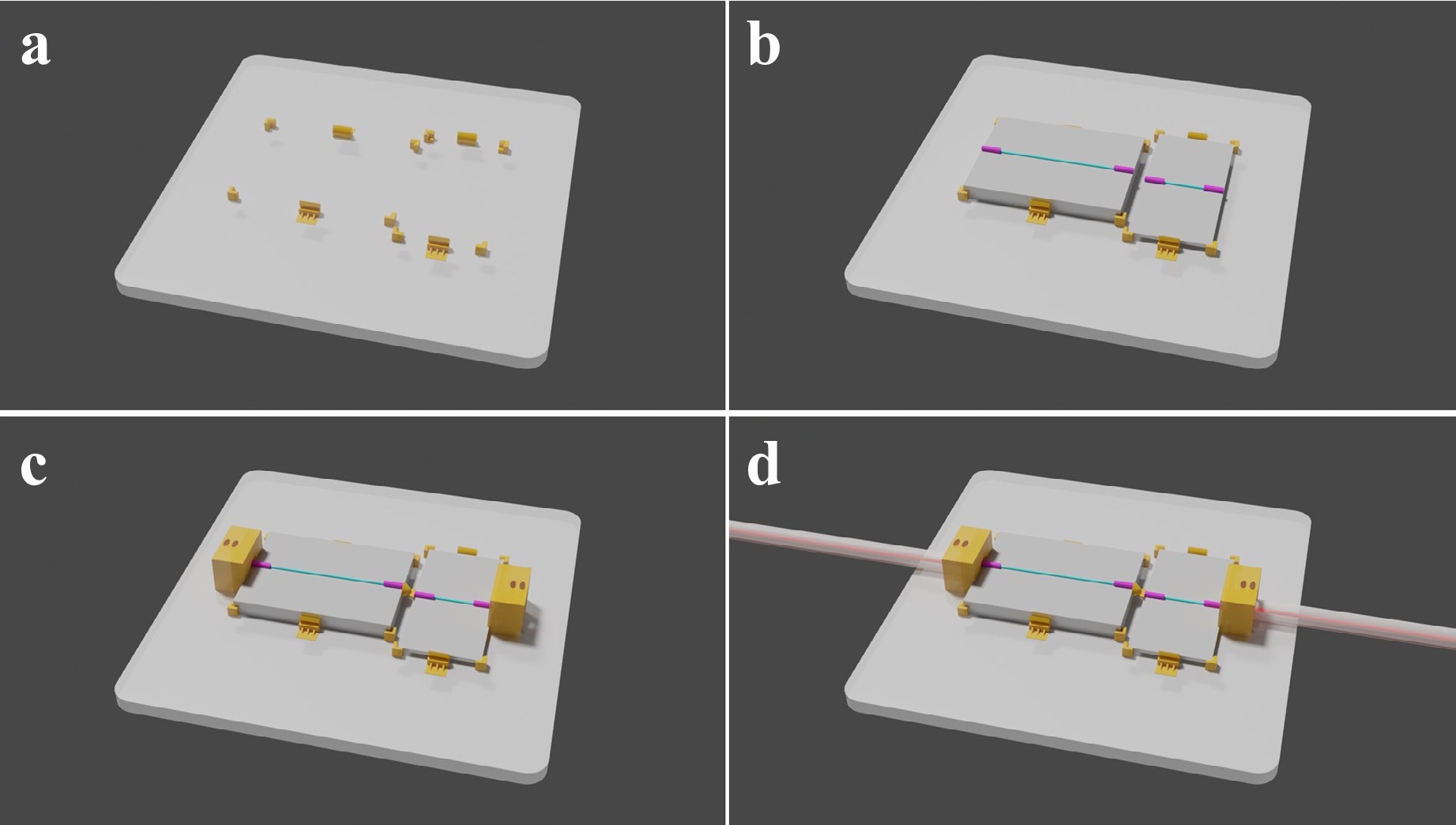
Fig. 6 Schematics of the process flow for the chiplet integration. The components are not in scale. a The fixers and clamps are printed on a silica substrate. Optional adhesives like crystalbond wax or UV glue can be applied21. b The chiplets are placed with the help of fixers. c Reflectors and the funnels are on-chip-printed. d I/O optical fibers are inserted and guided by the funnel structures.
We introduce an anti-reflection angle to the edge couplers on both chips which is often needed on gain-integrated chips (Fig. 4k). Two sets of fixers are printed on a silica substrate with relative positions to accommodate parabolic couplers, which form the framework of the optical interposer. Subsequently, the test chips are fixed onto the silica interposer, and the entire assembly is sent for a printing process wherein coupling units, including reflectors (Fig. 4l) and funnels, are printed onto the chiplets. A microscope image of the silicon-InP co-integration sample with fibers plugged in is shown in Fig. 7a, with close-ups of the key components. Fig. 7b schematically explains how the chip height difference is compensated with the couplers and the fixers.
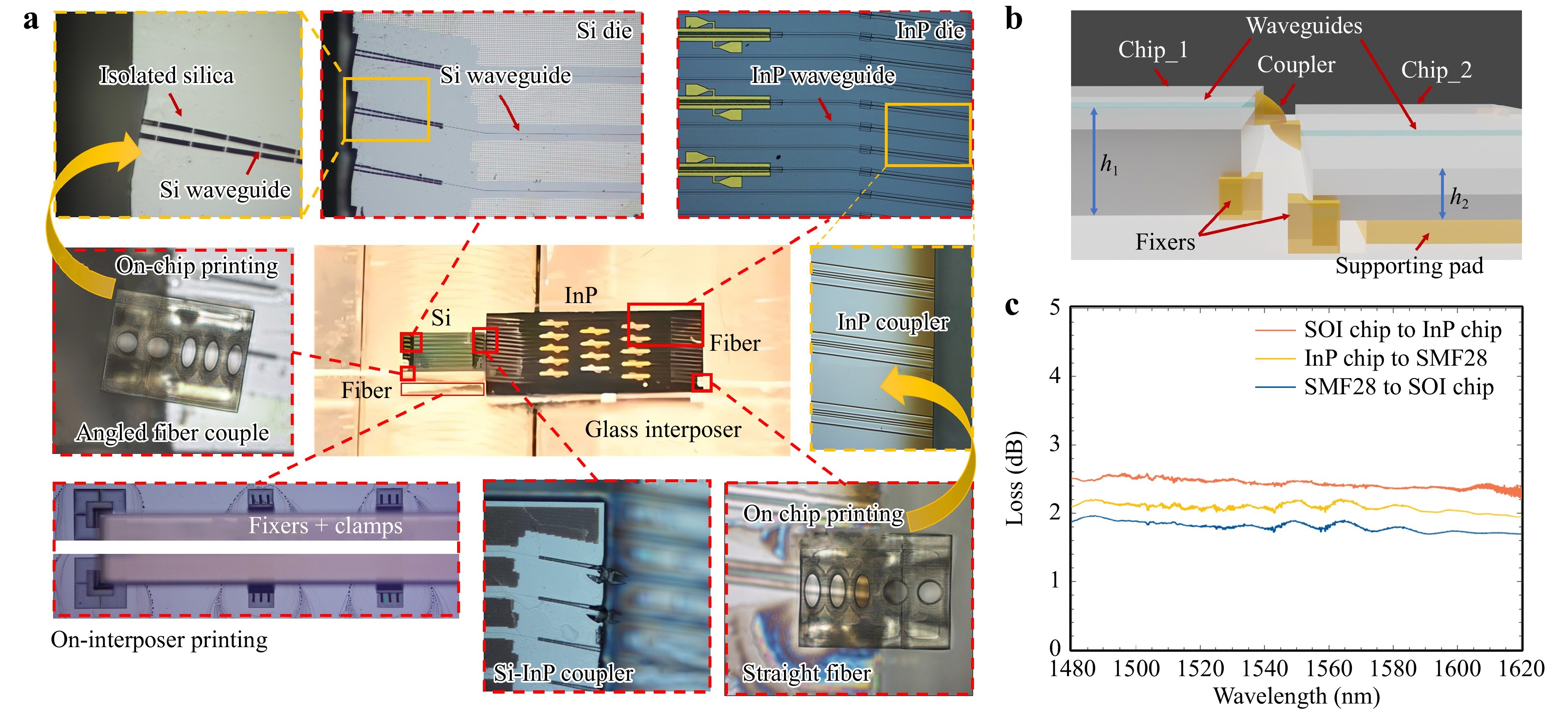
Fig. 7 Schematic of the coupling efficiency assessment for foundry-produced photonic chips. The SMF28 optical fiber, featuring a MFD of 10.4 µm, serves as the input path for the laser signal. The first coupler's funnel guides the fiber to the right position and adjusts the MFD to 7 µm to align with the silicon-based waveguide. Subsequently, the inter-chip coupler further shrinks the MFD to 5 µm, aligning with the III/V-based SOA array. The laser signal is then transmitted through the output fiber to a photodetector for measuring the output laser power, which is later used for the computation of coupler coupling loss.
For detailed characterization, the silicon and InP chips are assembled separately for the coupling loss breakdown. A tunable laser source (Keysight 81609A) sweeping from 1480 nm to 1620 nm is launched into the silicon, InP, and silicon-InP co-integration, respectively. The input and output of the chiplet connection are through two cleaved SMF28. By multiple tests of direct fiber-to-fiber coupling, reference power can be measured. After, the silicon and InP chip are placed into the loop and the power difference between input and output fiber is tested. The coupling efficiency of the couplers is determined by subtracting the reference loss and waveguide loss, which is given by the foundry, and detailed coupling loss is plotted in Fig. 7c. The measured coupling loss between the Si and InP chips is around 2.5 dB. The coupling loss between the fiber and the Si, and the fiber and the InP are slightly below 2 dB and over 2 dB, respectively. The excess loss is again mainly due to limited fabrication accuracy and its resulting misalignment. By improving the printing recipes and voxel size, as well as the reflector shape, the coupling loss can be effectively limited to below 1 dB. As we are trying to achieve a balance between performance and fabrication time, existing recipes are therefore adopted.
-
In this study, we introduce an adaptable yet powerful hybrid integration scheme that can interconnect photonic chiplets of different material systems, demonstrating both robust mechanical and optical performance. The pivotal contribution of our work lies in the demonstration of a compact photonic interposer that comprises both mode size converters and frames interconnecting waveguides of different material systems with zero change in established fabrication processes. This configuration is capable of ensuring passive alignment with minimal optical losses, despite current constraints in the fabrication accuracy.
This work so far focuses on photonic chip-let interconnections and the electrical connection aspect has not been demonstrated. However, in the envisioned system illustrated by Fig 1a, the electrical connections can be handled by the mature wire-bonding technique21. For a proper demonstration, this would require metallization on the glass interposer, which is a standard process but beyond our current capability. Alternatively, we would also envision that existing flip-chip-bonding technology22 can also be a good fit for our 3D-nanoprinted interposer solution to facilitate the fanout of high-density electrical connections. In this case, 3D-printing will be conducted on the substrate with dies flipped upside down, where visitable markers are needed. Another noteworthy consideration is thermal management. The incorporation of a heat sink or cooling pad is important, and the current silica substrates can be readily substituted with materials of high thermal conductivity, such as silicon. This allows direct mounting to a heat sink or cooling pad (Fig. 8b).
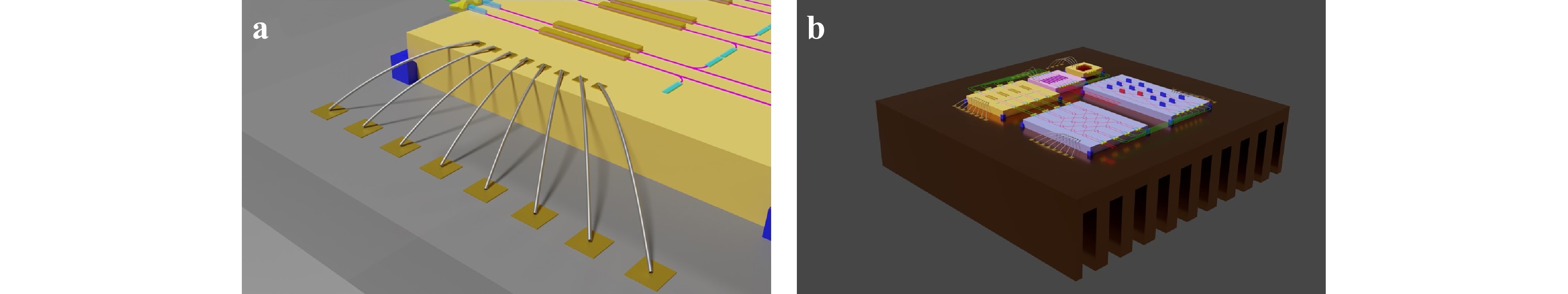
Fig. 8 Schematics of the future works. a Electrical connection with on-interposer metal contact pads. b Thermal management by using a heat sink as the substrate for the interposer.
The mode size converter, a fundamental component of our design, incorporates a pair of parabolic-shaped reflectors, which enables the unique capability of compressing or expanding the mode size with high coupling efficiency. To the best of our knowledge, we have achieved the largest mode size conversion ratio of 5:2 using non-waveguided components. The versatility of the parabolic-shaped coupler is demonstrated with angled placement, twisted rotation, polarization-insensitivity, and arrayed implementation, all of which exhibit comparable loss levels. We have also successfully implemented silicon-InP co-integration with plugged-in optical fibers using such an optical interposer. The excess loss mainly arises from the alignment variation due to the limited printing accuracy. This can be improved with a smaller voxel size, 200 nm at its finest23, of the two-photon polymerization tool, which will in turn improve the structure surface roughness. In addition, the phase delay which is partially responsible for the coupling loss can be further reduced by fine-tuning the reflecting surface and making them ‘free-form’19. Besides, we only explore the performance of the coupler at room temperature, the stability of the resin under harsh conditions (from −40 ℃ to 110 ℃)24 extends the potential of this work. To simplify the parabola design and facilitate a fast printing process, we stay with the perfect parabolic-shaped reflecting surface in this work. However, we foresee that coupling losses below 1 dB can be well achieved by making adequate improvements, making this hybrid integration approach hold great promise to stretch the limits of current PIC-level performance metrics without change of established process flows.
-
This work was supported in part by the UK EPSRC under grant QUDOS (EP/T028475/1), the European Union's Horizon Europe Research and Innovation Program under Agreement 101070560 (PUNCH), and European Union’s Horizon 2020 research and innovation program, project INSPIRE (101017088). The authors would like to thank the Cambridge EEDB for providing the facilities and professional support. We thank Dr. Tian Gu from MIT for his helpful advice on the fabrication.
Photonic chiplet interconnection via 3D-nanoprinted interposer
- Light: Advanced Manufacturing , Article number: (2024)
- Received: 24 January 2024
- Revised: 26 July 2024
- Accepted: 15 August 2024 Published online: 29 September 2024
doi: https://doi.org/10.37188/lam.2024.046
Abstract: In the past several decades, photonic integrated circuits (PICs) have been investigated using a variety of different waveguide materials and each excels in specific key metrics, such as efficient light emission, low propagation loss, high electro-optic efficiency, and potential for volume production. Despite sustained research, each platform shows inherit shortcomings that as a result stimulate studies in hybrid and heterogeneous integration technologies to create more powerful cross-platform devices. This is to combine the best properties of each platform; however, it requires dedicated development of special designs and additional fabrication processes for each different combination of material systems. In this work, we present a novel hybrid integration scheme that leverages a 3D-nanoprinted interposer to realize a photonic chiplet interconnection system. This method represents a generic solution that can readily couple between chips of any material system, with each fabricated on its own technology platform, and more importantly, with no change in the established process flow for the individual chips. A fast-printing process with sub-micron accuracy is developed to form the chip-coupling frame and fiber-guiding funnel, achieving a mode-field-dimension (MFD) conversion ratio of up to 5:2 (from a SMF28 fiber to 4 µm × 4 µm mode in polymer waveguide), which, to the best of our knowledge, represents the largest mode size conversion using non-waveguided 3D nanoprinted components. Furthermore, we demonstrate such a photonic chiplet interconnection system between silicon and InP chips with a 2.5 dB die-to-die coupling loss, across a 140 nm wavelength range between 1480 nm to 1620 nm. This hybrid integration plan can bridge different waveguide materials, supporting a much more comprehensive cross-platform integration.
Research Summary
3D photonics integration: chip level connection via 3D nanoprinting
Photonics integrated circuits (PICs) are now being widely utilized in variety of field including optical communication, optical computing, biological sensing, etc. Based on different material platforms, each platform shares its own advantages over the others, which makes heterogeneous integration a vital task in broader use of PICs. Qixiang Cheng from University of Cambridge and colleagues now report a fibre and chip level scale integration enabled by two photon polymerization of polymers. By directly fabricating the device onto as-fabricated chips, this technology can match the dislocation and mode size among different PIC platforms without damaging their own original structure. The team demonstrate the optical interconnection on fibre-to-fibre, fibre-to-chip and chip-to-chip applications, which provide a novel approach for future large scale heterogeneous integration.
Rights and permissions
Open Access This article is licensed under a Creative Commons Attribution 4.0 International License, which permits use, sharing, adaptation, distribution and reproduction in any medium or format, as long as you give appropriate credit to the original author(s) and the source, provide a link to the Creative Commons license, and indicate if changes were made. The images or other third party material in this article are included in the article′s Creative Commons license, unless indicated otherwise in a credit line to the material. If material is not included in the article′s Creative Commons license and your intended use is not permitted by statutory regulation or exceeds the permitted use, you will need to obtain permission directly from the copyright holder. To view a copy of this license, visit http://creativecommons.org/licenses/by/4.0/.

 DownLoad: