


-
Since their discovery, perovskite materials have been widely used in various fields, including energy and information storage, optoelectronics, and lasers, owing to their unique optical and electrical properties1–3. Different forms of perovskites have different functions and can therefore be widely applied in various fields. For example, perovskite quantum dots (PQD) are widely used in narrowband emission optical pressure sensor systems and displays4,5. Nanowire perovskites with excellent optical and electrical properties are often used in photodetectors and sensors6–9, and high-quality patterned 2D perovskite films are generally used in perovskite solar cells10,11. Improving the preparation, processing quality, and efficiency of perovskite materials has become a major focus in these applications.
Perovskite materials may be prepared in a number of ways, such as salt decomposition12, solid phase13,14, hydrothermal synthesis15, and sol-gel methods16. However, each method has drawbacks. For example, the salt digestion method is not suitable for the preparation of pure samples, the solid-phase method requires higher temperatures, resulting in higher energy consumption, and the sol-gel method is expensive and the produced samples are not very stable17. Recently, with the rapid development of femtosecond laser technology, shorter pulse widths and higher peak powers have become accessible, and can further reduce the thermal effect and improve precision during material processing using femtosecond pulses18. Hence, femtosecond lasers are powerful tools for preparing perovskite materials of different shapes, sizes, and complex structures.
The resolutions, applications, advantages, and disadvantages of various patterned fabrication methods are listed in Table 1. Methods such as focused ion beam etching19, inkjet printing20,21, and physical templates22 used in perovskite processing do not satisfy the precision requirements of ultrahigh-density devices and novel optical structures. Although nanoimprinting can accomplish nanoscale precision, material limitations can restrict the process which is susceptible to damage from molds and material pressure23,24. By contrast, femtosecond laser processing offers a wide range and programmable nanoscale precision machining without the need for masks25,26. Inevitably, femtosecond laser direct-writing technology has certain drawbacks, such as expensive equipment, complex optical paths, and optical diffraction limits27. The rapid development of femtosecond laser technologies, which will facilitate the development and innovation of femtosecond lasers in the fields of micro-and nanoprocessing should address the current limitations.
Processes involved Resolution Application Advantage Disadvantage Ref. Focused ion beam etching µm Solar cell Direct writing
High resolutionLow throughput
High-cost equipment19 Inkjet printing µm Photodetector Simple process
High-throughputLow resolution
Nozzle blocking20, 21 Physical template µm Solar cell
PhotodetectorSimple principle Need templates
Restrictions
High-cost equipment22 Nanoimprinting nm Lasers
NanogratingHigh-throughput
Large areaLimited materials
Damage from pressure23, 24 Femtosecond laser processing nm Lasers
Solar cell
Photodetector
NanogratingTemplate-free
Wide range of applications
Programmable operationHigh-cost equipment 25, 26 Table 1. Resolution, application, and advantages and disadvantages of various patterned manufacturing methods
In this review, we first introduce the principles and parameters of femtosecond-laser-induced precipitation of perovskites and provide detailed information on the advantages and applications of this technology. Second, we introduce various types of femtosecond laser processing for perovskite materials and discuss, in detail, the advantages and existing problems of this technology. Finally, we provide an outlook on the basic challenges of femtosecond laser preparation and processing methods for perovskites and important and promising directions for future research.
-
Perovskite materials are a class of materials characterized by a distinctive crystal structure and exhibit a range of advantages, including high absorption and charge mobility28, superior photoelectric conversion efficiency29, ease of synthesis and processing30, multifunctionality, and a degree of thermal stability31. Consequently, perovskites have found widespread applications in information storage32, optoelectronic detectors33,34, displays23, solar cells35, light-emitting diodes (LED)15,36, and lasers3,37, ensuring they are well-researched. Currently, the methods for synthesizing perovskite-structured compounds include the traditional high-temperature solid-phase and sol-gel methods, and hydrothermal synthesis38. The high-temperature solid-phase method is the most widely used and is suitable for large-scale production of materials with low purity requirements. High-purity and small-particle-size products are accomplished using the sol-gel method owing to its simplicity and low reaction temperature. However, the method does have drawbacks, which include significant shrinkage and susceptibility to pore formation, that reduce the density of the products during processing. For perovskite materials, increasing the density can minimize energy loss, enhance the charge carrier transport efficiency, and bolster the resistance to external factors such as moisture and oxygen. However, eliminating these pores requires additional experimental steps, leading to increased production costs. Hydrothermal synthesis is better suited to preparing ultrafine, non-aggregated, or less-aggregated materials, and perovskite materials such as single-crystal spherical core-shell materials. However, the technique is not suited to the preparation of water-sensitive starting materials. These preparation methods typically produce perovskites directly in air. As perovskites are sensitive to temperature and air humidity39–41, exploring methods to improve their photostability and restore their properties after destruction is of great significance. Femtosecond lasers offer an economical and convenient method to induce crystallization of micro-and nanocrystals (NCs) in transparent materials (glass and single crystals). Moreover, femtosecond lasers can selectively remove and regenerate these materials through further irradiation and thermal treatment. Femtosecond laser irradiation can instantaneously generate high-temperature plasma in the focal region via nonlinear multiphoton absorption and photon-matter interactions, providing a reliable and efficient method to produce perovskite42.
In 2016, Chou et al.43 first accomplished the crystallization of halide perovskites using a laser with a frequency of 80 MHz and pulse duration of 60 fs, as shown in Fig. 1a. The researchers used the inverse correlation between perovskite solubility and temperature to induce perovskite crystallization using localized heating of the substrate; the localized heating was induced by laser irradiation. This method provided a new approach to perovskite crystallization and offered new perspectives for future perovskite studies. In the following year, Arciniegas et al.44 also induced the growth of perovskite crystals using femtosecond laser irradiation, as shown in Fig. 1b. Plate-like structures, in a donut shape, up to 25 µm in size, formed at a high power, while very few compact and smaller platelets grew around the irradiated region at reduced laser power (less than 250 mW). Below 180 mW, laser-induced crystal growth was not observed. Arciniegas et al. changed the shape and size of the perovskite crystals by adjusting the laser power density or irradiation time and analyzed the effect of the laser irradiation dosage on the induced perovskite crystals in detail (Fig. 1c). A continuous line comprising perovskite crystals was obtained by moving the laser beam at a constant power of 370 mW and speed of several millimeters per second (Fig. 1d). The conductivity of the continuous line was measured to verify its potential for optoelectronic applications.
Fig. 1 Femtosecond laser-induced synthesis of perovskite. a Schematic illustration of femtosecond laser-induced CH3NH3PbBr3 perovskite crystallization. Reproduced with permission43. Copyright 2016, American Chemical Society. b Sketch of laser printing process. c Color fluorescence image captured after laser irradiation, indicating the changes in size and distribution of the induced MAPbBr3 crystals upon varying the laser power and exposure time. d Color fluorescence image of MAPbBr3 wire prepared at different displacement speeds. Reproduced with permission44. Copyright 2017, Wiley-VCH. e Schematic illustration of femtosecond laser writing system used for sample fabrication. f Optical images of CsPbBr3 quantum dots (QDs) array under ultraviolet (UV) irradiation during erasing-restoration process (top) and intensity mapping of readout signal (bottom). Reproduced with permission45. Copyright 2019, Nature Photonics.
The data explosion has driven the development of storage fields, accelerating exploration of novel data storage media with high switching speeds, large storage capacities, low power consumption, and long service lives. To further enhance data storage capacity, a new method to reversibly fabricate perovskite materials for high-capacity optical data storage or information encryption has gradually become a research focal point. Dong et al. conducted extensive exploration of the experimental aspects of femtosecond laser-induced perovskite crystallization in glass for data storage and information encryption. In 2019, Dong et al.45 induced perovskite crystallization in glass doped with Cs, Pb, and Br using an 800 nm femtosecond laser, as shown in Fig. 1e. The growth of the CsPbBr3 QDs was confirmed by luminescence, transmission electron microscopy (TEM), and high-resolution transmission electron microscopy (HRTEM) images, as well as the size and photoluminescence (PL) intensity of the constructed regions. The distribution of CsPbBr3 QDs could be customized based on the laser power density and exposure time, and velocity of the sample-stage. In addition, green emission could be immediately eliminated by further femtosecond laser irradiation (Fig. 1f) and could be completely recovered after low-temperature annealing. Subsequently, Dong et al. conducted further research on rewriting, and first induced the formation of CsPb(Cl/Br)3 NCs in glass using a femtosecond laser, which was verified by observing the appearance of red-shifted PL peaks46. The researchers selectively induced the removal and regeneration of 3D luminescent patterns by using femtosecond laser irradiation combined with thermal treatment. Fig. 2a shows nine cycles of the laser erasing and recovery processes, demonstrating the reversibility of the perovskites and the switchable PL inside the glass. Furthermore, Li et al.47 conducted similar erasure-recovery experiments, and induced the reversible crystallization of CsPbBr3 NCs using a femtosecond laser; in addition, the researchers demonstrated the generation, erasure, and regeneration of PL patterns with micrometer-level resolution in CsPb2Br5 single crystals. This technology is expected to promote the application of perovskites in displays, information encryption and decryption, anti-counterfeiting technology, high-capacity optical data storage, 3D commercial art, and information security. A method for encryption using the reversible PL of perovskite materials has been developed.
Fig. 2 Applications of femtosecond laser-induced perovskite in storage and display directions. a Photoluminescence (PL) intensity, PL peak position, and full width at half maximum (FWHM) of CsPb(Cl/Br)3 NC in glass recorded during nine consecutive erasing/restoring cycles. Reproduced with permission46. Copyright 2020, American Chemical Society. b Polarization perovskite quantum dots (PQD) pattern written by laser into a line array. c Schematic illustration of multilayer quantum dots (QD) pattern written by laser onto glass with polarization emission. Reproduced with permission48. Copyright 2023, Wiley-VCH. d Schematic illustration of ultrafast laser direct-writing system used for CsPbBr3 quantum dot-doped glass optical storage. e Writing and readout of optical information in the glass, showing its potential as a data storage medium with high data reading accuracy. f Demonstration of reversible 3D optical data storage. Reproduced with permission49. Copyright 2022, Wiley-VCH. g Mapping of photoluminescence signal intensity of CsPbI3 QD array during UV erasing-rewriting process and schematic illustration of multilayer optical storage application. h Optical image of QD line written by ultrafast laser. Reproduced with permission58. Copyright 2021, Wiley-VCH.
Polarization modes exhibit advantages such as high security, fast response, simple operation, and strong selectivity, that are crucial for improving resolution and enhancing anti-counterfeiting technology. Dong et al.48 investigated the formation of PQD structures in glass under the polarization modes induced by a femtosecond laser. A polarization structure of CsPbBr3 QDs with a polarization degree of up to 0.189 was fabricated in a transparent glass matrix, and a strategy for 3D polarization-sensitive optical anti-counterfeiting was implemented. The effects of the line width and spacing on the degree of polarization were first studied. Subsequently, 2D and 3D polarization luminescence patterns composed of vertical and horizontal lines were created inside the glass, as shown in Fig. 2b. By utilizing polarized emission, different layers with distinct polarization angles could be used for anti-counterfeiting on a 3D scale. For example, under vertical polarization, insufficient disparity in the PL intensity between the vertical and horizontal line patterns rendered the information of the quick response (QR) code unidentifiable. The QR code could only be clearly displayed and recognized under horizontal polarization. Furthermore, to demonstrate that this method could be used for 3D polarization optical anti-counterfeiting, the researchers created a 3D polarization-laminated structure. Under 447 nm laser illumination, the "heart" pattern composed of vertically and horizontally aligned CsPbBr3 QD lines exhibited unpolarized and different polarization angles (Fig. 2c). Optical images with different polarization directions can be used for anti-counterfeiting on a 2D scale. In summary, femtosecond-laser-induced perovskite precipitation of different anti-counterfeiting patterns facilitated the design and manufacture of high-precision intelligent anti-counterfeiting devices.
Soon after, Sun et al. discovered that the technology developed by Dong required long write times, ranging from several hundred milliseconds to several seconds, when recording data. Longer write times result in a higher power consumption49. The core issues affecting the application value for optical data storage technology have always been reducing power consumption and increasing write speed. Sun et al. discovered that the information recorded by precipitated CsPbX3 (X = Cl, Br, I) QDs was clearly visible on the dark background of an unprocessed glass matrix, which is not conducive to highly secure information encryption. However, Dong et al. discovered that using a lower laser power and shorter irradiation time could considerably decrease the luminescence of CsPbX3 QDs. Sun et al. proposed a strategy for weakening the luminescence of CsPbX3 QDs to accomplish high-speed, low-power 3D optical data storage. The researchers used femtosecond laser irradiation to address the luminescence degradation of PQDs and accomplished fine modulation of the photoinduced luminescence by adjusting the laser parameters such as laser power, repetition rate, and pulse duration. The data were written onto glass through high-repetition-rate laser irradiation (Fig. 2d) and read out as locally darkened PL images under 485 nm excitation. In addition, Sun et al. conducted “write-erase” cycling experiments to demonstrate the reversible data storage capacity of this technology. Finally, they used a focused laser beam with a repetition rate of 100 kHz, pulse width of 380 fs, and pulse energy of 600 nJ to create QR codes and other images (Fig. 2e). In response to the development trend of 3D optical data storage, optical information is written at arbitrary positions inside glass. The dark photoluminescent patterns of “cherry blossoms, lotus flowers, and tulips” written at different depths in glass are illustrated in Fig. 2f. After thermal treatment (470 °C, 120 min), the patterns were erased and rewritten in situ as cartoon patterns of “dragonflies, bees, and smiling faces.” This technology was able to prevent interlayer crosstalk when the layer spacing was 30 µm. Therefore, this technology has broad application prospects in high-density 3D optical data storage, anti-counterfeiting markers, and other optoelectronic applications.
The incorporation of PQDs into glass can significantly improve its chemical and thermal stabilities, with a photoluminescence quantum yield (PLQY) as high as 80%50. PQDs may be used in displays, information storage, photodetectors, and lasers51–55. High-resolution PQD fabrication techniques are required to realize miniaturized displays. However, traditional techniques, such as photolithography and inkjet printing, cannot meet the requirements of high resolution and stability56,57. Sun et al.58 directly wrote CsPbI3 QDs with deep-red photoinduced luminescence inside glass via femtosecond laser-induced thermal effects, with an internal quantum efficiency of 23%, in an unprecendented instance of direct writing of deep-red fluorescent CsPbI3 QDs in glass. The researchers further demonstrated the ability to erase and rewrite CsPbI3 QDs in glass without thermal treatment by controlling the thermal accumulation during the femtosecond laser-writing process, and by revealing the multi-layer writing of CsPbI3 QDs in glass (Fig. 2g). Additionally, they accomplished photoinduced luminescence lines with submicrometer linewidths from the CsPbBr3 QDs. Fig. 2h shows the optical and corresponding emission images of fabricated lines with a repetition frequency (RF) between 20 to 70 kHz with a writing speed of 10 µm s−1. The lines become increasingly homogeneous with an increase in RF because the thermal accumulation effect is enhanced and the injected pulse number per unit length is increased. This technique for producing highly stable linear and nonlinear optical properties in linear and nonlinear optical devices promotes the application of PQDs in this field. In addition to femtosecond lasers that induce the precipitation of PQDs, nanosecond lasers can also enable the on-site fabrication and direct laser writing of PQDs59. Zhan et al.60 used a 405 nm nanosecond laser to fabricate gamma-phase CsPbI3 QD patterns and demonstrated bright photoinduced luminescence emission with a quantum yield as high as 92%. Moreover, the researchers achieved a minimum linewidth of 900 nm and constructed an emitting grating with a period of 4 µm. Therefore, multiple methods are available for PQD fabrication.
In the field of display applications, Liang et al.61 synthesized high-resolution patterned red (R), green (G), and blue (B) PQDs using a femtosecond laser with a center wavelength of 800 nm, pulse width of 100 fs, and frequency of 80 MHz. The fluorescence microscopy images of the R/G/B microfibers and triangular arrays exhibited similar linewidths, good uniformity, and clear boundaries (Fig. 3a). The mechanism is based on the optothermoelectric effect of the Marangoni flow induced by the laser to aggregate and deposit PQDs (Fig. 3b). Liang et al. accomplished a minimum linewidth of 1.58 µm by adjusting the laser power and exposure time; a feat that is significant for the application of PQDs in high-resolution displays. Finally, the reasearchers compared the ability of different methods to produce minimum linewidths for R/G/B materials (Table 2). Femtosecond laser direct-writing (FsLDW) technology has significant advantages in terms of manufacturing precision and full color. In addition, using pure blue light in the range between 460–470 nm as one of the primary colors is crucial for high-quality full-color displays62–64. Sun et al.65 used a femtosecond laser to fabricate pure blue light-emitting perovskite nanocrystals (PNCs) in borosilicate glass containing Cs, Pb, Cd, and halide elements. The prepared pure blue-light emitting CsCdxPb1-xBr3 PNCs accomplished a PLQY of 13.4% and were stable under 40 W cm−2 of UV radiation. Furthermore, the bandgap of the perovskite in glass could be adjusted by changing the composition of B and X elements in the ABX3-type perovskite. The emission wavelengths in the range between 461–520 nm could also be tuned by adjusting the chemical composition of the Cd/Pb mixed cation system at site B.
Fig. 3 Femtosecond laser synthesis: perovskite display advancements in direct writing and holography. a R/G/B tricolor fluorescence microscopy image. b Schematic of laser direct-writing deposition of perovskite quantum dots (PQDs) and pattern of laser deposition of PQDs under UV light irradiation with an optical fluorescence microscope. Reproduced with permission61. Copyright 2022, The Royal Society of Chemistry. c Long persistent luminescence performance and corresponding photonic characteristics of CsPbBr3 perovskite-based gas chromatography systems doped with 0.9% La3+, 0.9% Dy3+, and 0.9% Nd3+ ions, along with images captured post 10 s fs irradiation, are presented (upper), accompanied by a gas chromatography platform for optical information processing (middle) and the schematic illustration of the recorded optical information (lower). Reproduced with permission70. Copyright 2022, Wiley-VCH. d Direct photolithography of composition-tunable PNCs in glass. e Photoluminescence stability test. f Directly lithographed PNC patterns and demonstration of a dynamic holographic display. Reproduced with permission59. Copyright 2022, Science.
Table 2. Comparison of preparation methods for patterned NC fluorescent materials
Existing magnetic storage devices are short-lived and energy-intensive; however, optical storage does not have these limitations. The long persistent luminescence (LPL) of CsPbBr3 NCs is an optical storage phenomenon with extensive application prospects in fields such as chemical sensing, biological imaging, and information encryption. However, accomplishing LPL at room temperature remains challenging. Peng et al.70 successfully accomplished room-temperature LPL in CsPbBr3 microcrystalline glass ceramics (GCs) using femtosecond laser writing technology. Additionally, the researchers successfully doped CsPbBr3 GCs with La3+, Dy3+, Nd3+, and Lu3+ ions to flexibly adjust the LPL performance and discussed the corresponding mechanism in detail. Using CsPbBr3 GCs with high recognition capability, a time-resolved information encryption model was successfully proposed (Fig. 3c), and the obtained CsPbBr3 GCs were reusable and had high color purity (97.04%). This outcome confirms the potential applications of CsPbBr3 GCs perovskites in optical storage, advanced anti-counterfeiting, and nonlinear optics. Sun et al.59 accomplished direct 3D femtosecond laser lithography of PNCs with a tunable composition and bandgap in a halide-oxide composite glass containing Cl−−Br−−I− (Fig. 3d). The NCs were exceptionally stable under UV irradiation, organic solvent soaking, and high-temperature environments. As shown in Fig. 3e, there was no change in the PL intensity after 12 h of UV exposure. The PNCs remained stable without any change in the PLQY 6 months after being dispersed in ethanol. The PL intensity and position of PNCs also remained as the initial characteristics after they were heat-treated at 85 °C for 960 hours. In addition, the researchers demonstrated the application of this 3D structured nanomaterial in optical storage, micro-LEDs, and holographic displays (Fig. 3f). These results reveal developmental prospects in the field of optical storage and indicate the direction of future information storage technology.
The emergence of low-energy edge states (LESs) in perovskites provides a new perspective for improving their optoelectronic properties, because LESs could be key to enhancing the performance of quasi-2D perovskite optoelectronic devices. However, the formation mechanism of LESs is not fully understood and is difficult to control. Miao et al.71 induced the formation of LESs in quasi-2D (BA)2(MA)n-1PbnI3n+1 (n > 1) single crystals using femtosecond laser ablation. Time-resolved photoluminescence (TRPL) spectra, scanning electron microscopy (SEM), and energy-dispersive X-ray spectroscopy (EDS) of multiple samples indicated that the LESs induced by laser ablation originated from 3D MAPbI3 PNCs, which lost or replaced the BA ligand and formed at the edge of the irradiation trace. In addition, the researchers compared the optical and morphological properties of the samples before and after femtosecond pulsed and continuous-wave laser ablation. Compared with the previous random application of the LESs method, Miao et al. provide a higher spatial resolution and higher control accuracy of the LESs fabrication method, offering more opportunities for the development of high-performance quasi-2D perovskite optoelectronic devices.
Currently, all-inorganic CsPbBr3 PNCs are widely used in applications such as lasers, LEDs, and information encryption. However, self-crystallization of PNCs inside glass before further thermal treatment significantly hinders their application in data storage. Jin et al.72 first proposed the use of a melt-quenching method to adjust the ZnO (4–20 mol%) to suppress self-crystallization of perovskite crystals. By comparing five glass samples with different ZnO contents, it was found that when the ZnO content was 4% (sample 5), the CsPbBr3 NCs did not self-crystallize inside the glass and exhibited a colorless state (Fig. 4a). Subsequently, the researchers demonstrated the application of sample 5 in optical information storage by combining an 800 nm femtosecond laser and annealing (920 h−1) processes (Fig. 4b). They first used fs-induced crystallization (50 mW, 5 s) and annealing for point crystallization, where the green dots represent logical binary state 1 and the uncrystallized areas represent 0. Subsequently, laser erasing was performed to modify the data. This process demonstrates the enormous potential of perovskites for rewritable information storage inside glass and the excellent stability of the sample in water and ethanol.
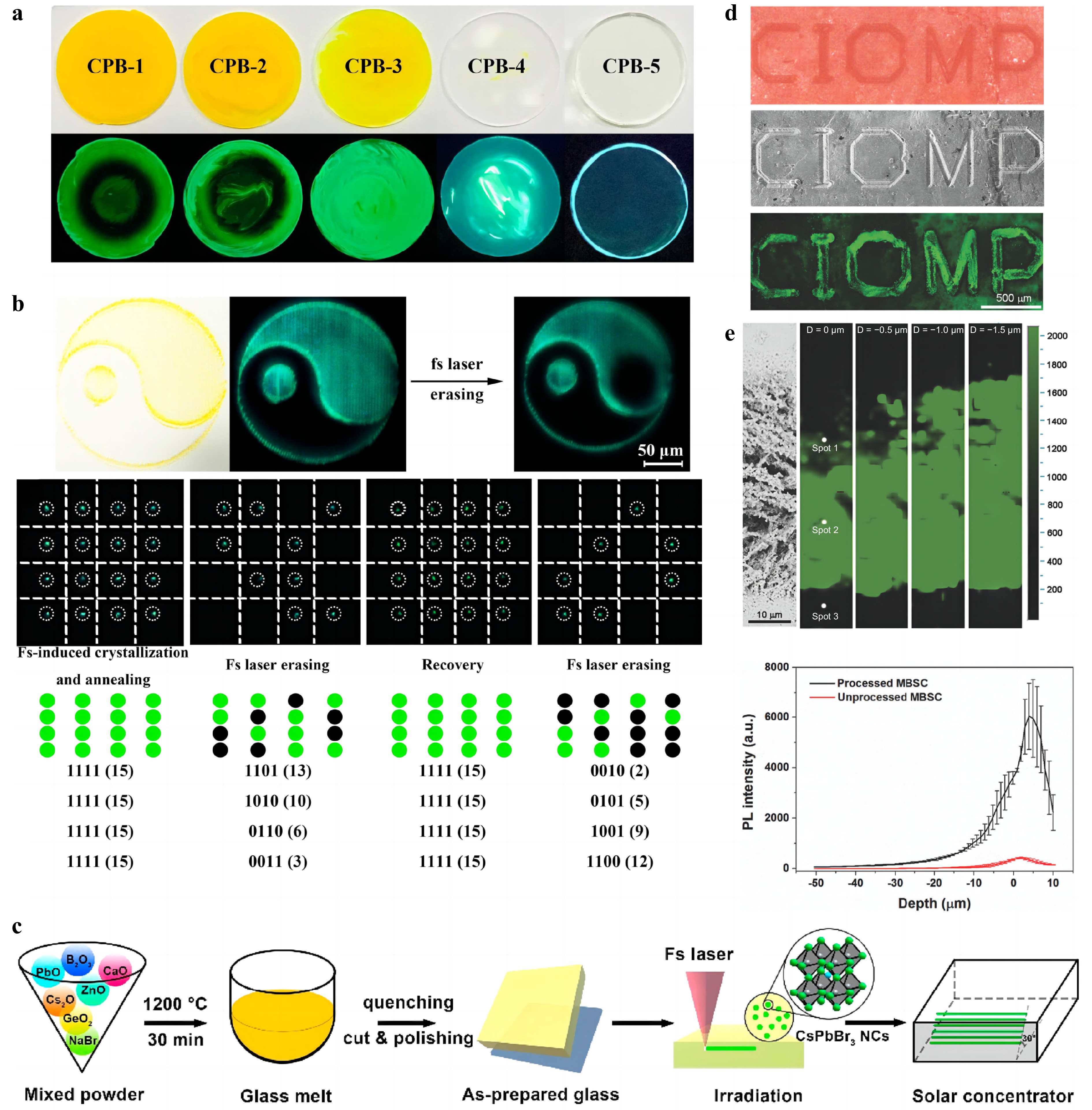
Fig. 4
Examples of femtosecond laser-driven synthesis of perovskites and their applications in display and optical storage technologies. a CPB-1, CPB-2, CPB-3, CPB-4, and CPB-5 subjected to non-thermal treatment under sunlight and 365 nm UV light. b The process of drawing a Tai Chi diagram inside the glass and application of CPB-5 in optical information storage. Reproduced with permission72. Copyright 2022, Chemical Engineering Journal. c Schematic of CsPbBr3 perovskite nanocrystals precipitated in glass, prepared and induced by femtosecond laser irradiation. Reproduced with permission73. Copyright 2019, American Chemical Society. d Optical, scanning electron microscopy (SEM), and photoluminescence (PL) images of the word “CIOMP” fabricated via femtosecond laser processing. e SEM and PL images of MAPbBr3 single crystals treated at different depths (0 to −1.5 μm) in ambient air, along with the relationship between PL intensity and depth in processed and unprocessed regions at various depths. Reproduced with permission74. Copyright 2018, WILEY-VCH. Other researchers have explored femtosecond-laser-induced perovskite synthesis from different perspectives. Hu et al.73 realized the spatial and size-controlled precipitation of CsPbBr3 PNCs using direct femtosecond laser writing, and used a glass containing GeO2/B2O3/ZnO/CaO/PbO/Cs2O/NaBr for femtosecond laser processing and thermal annealing (Fig. 4c). The researchers accomplished fluorescence across the blue to green range, and these PNCs exhibited brighter fluorescence after secondary annealing.
In addition to inducing the precipitation of perovskite, femtosecond lasers can modify the properties of perovskite by tuning its optical properties, reducing nonradiative recombination losses, and altering its crystal structure74–78. The PL intensity of single-crystal perovskites is much weaker than that of polycrystalline perovskites, and deficiencies exist in PL-related applications. To address this limitation, Xing et al.74 used a femtosecond laser to act on an MAPbBr3 single crystal and accomplished an increase in the PL intensity that was greater by two orders of magnitude in air and three times greater in N2 gas. As shown in Fig. 4d, the region outside the processing region was not damaged, and the PL brightness in the processing area was higher than that in the unprocessed area. The PL intensity in the processing region was significantly greater than that in the unprocessed area (Fig. 4e). Additionally, the researchers discovered that femtosecond laser pulse-induced micro/nanostructures on the surface of perovskite single crystals could significantly enhance their PL intensity. The PL enhancement was attributed to photon cycling caused by the laser-induced texture, light output coupling mechanism, and surface recombination center passivation caused by micro/nanostructures. This original approach for accomplishing PL enhancement in perovskite single crystals should find extensive applications in luminous or PL imaging devices in the near future.
-
Laser devices based on halide perovskites have become powerful tools in modern nanophotonics, and nanowire-shaped nanocavities are among the most popular cavity shapes in perovskite single-particle lasers. The primary methods for producing nanowires are chemical vapor deposition (CVD)79 and wet chemical methods80. In addition, nanopatterning using high-throughput laser ablation methods can preserve the luminescence properties of materials, which may be degraded using traditional lithographic methods. Halide perovskite nanowires are excellent nanomaterials for waveguide PL and lasers80,81. Owing to their low thermal conductivity82 and high defect tolerance83, high-throughput direct laser writing of nanogratings on their top surfaces is possible. Using this technology, Alexey et al.25 demonstrated semiconductor nanowire lasers with highly directional vertical coupling and directly wrote in-depth subwavelength (260 nm period) gratings on CsPbBr3 perovskite. This grating could generate vertical coupling in the nanowire cavity with a divergence angle of approximately 2°. Furthermore, the researchers discovered that the mode selection performed by the resulting nanogratings narrowed the laser peak spectrum by a factor of two without increasing the laser threshold, and significantly improved the performance of perovskite lasers.
The commercialization of perovskite solar cell technology requires further improvements in conversion efficiency. Among the methods used for improving conversion efficiency, laser scribing is used to upgrade small-area perovskite solar cells into large-area solar modules to accomplish an integrated interconnection between individual solar cells. Scribing methods can be performed using mask templates, chemical etching, or mechanical and laser scribing techniques. Because the functional layer typically contains a perovskite thin film and laser scribing can produce finer scribed areas, laser scribing predominates. Simultaneously, the quality of scribing in the functional zone of perovskite solar cells can affect the final performance of the solar component84. To ensure good performance of the scribed solar cell and complete removal of the functional layer without damaging the conductive substrate, Wang et al.83 used a 1030 nm wavelength femtosecond laser to scribe P2 (Fig. 5a), and reduced material waste and production costs. When laser pulses interact with target materials, energy first excites electrons within the material, which are then converted to thermal energy through electron-phonon scattering. During the material removal processes, the influence of thermal energy is determined primarily by the relationship between the pulse duration and electron-phonon coupling time85. Nanosecond pulses provide sufficient time to transfer energy to the lattice phonons, causing the material to melt or even vaporize. By contrast, femtosecond-pulse lasers deposit energy at a much faster rate, causing materials to rapidly convert to vapor or plasma, resulting in a process known as cold ablation with a small thermally affected zone and excellent precision. However, the high cost of femtosecond laser systems has limited their widespread adoption in large-scale commercial applications. Picosecond pulse lasers, by contrast, bridge the gap between femtosecond and nanosecond lasers, with pulse durations close to the coupling time. Compared with femtosecond lasers, picosecond laser systems are cheaper and more suitable for certain economic demands. Notably, the quality of scribing in the functional zone of perovskite solar cells directly affects the performance of the solar component. Therefore, optimization of scribing techniques is crucial for improving the performance of solar cells.
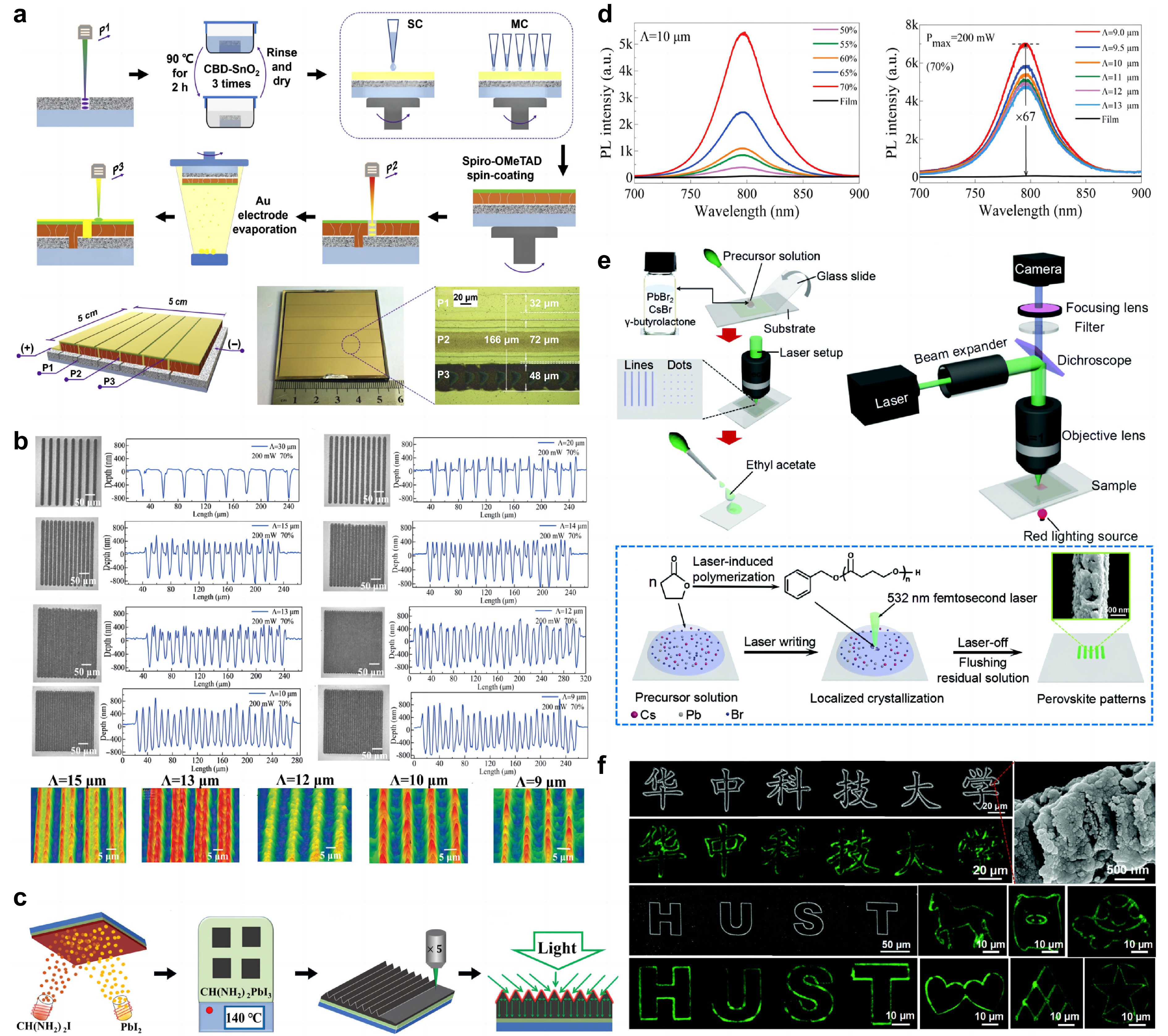
Fig. 5 Laser preparation of perovskite microstructure and its optical properties. a Manufacturing process of laboratory mini-modules. Reproduced with permission83. Copyright 2020, Journal of Power Sources. b Optical microscope images and corresponding cross-sectional height maps of FAPbI3 perovskite gratings with different periods. c Schematic diagram of laser-induced optical moment in FAPbI3 grating microstructures. d Optical properties and physical mechanisms of perovskite gratings. Reproduced with permission88. Copyright 2022, Wiley-VCH. e In-situ formation of Cs-Pb-Br nano composites via organic solvent polymerization using 532 nm femtosecond laser pulses. f In-situ fluorescence and laser-patterned Cs-Pb-Br nano composites. Reproduced with permission89. Copyright 2020, The Royal Society of Chemistry.
Perovskite triangular subwavelength gratings (SWG) exhibit low reflectance, high absorption, and excellent emission characteristics that can enhance the light-capturing capabilities of solar cells and photodetectors86,87. However, manufacturing irregular perovskite SWG with high crystal quality and good optical properties remains challenging. Tian et al.88 used the precise spatial and power control of femtosecond laser processing to fabricate an FAPbI3 perovskite SWG. A schematic of the triangular-grating microstructure fabrication method is shown in Fig. 5c. The researchers studied the optical properties and physical mechanisms of the perovskite gratings with different structural parameters (period and depth). The grating achieved a uniform depth (approximately 800 nm) (Fig. 5b), which indicates a stable manufacturing process. To understand the optical properties of laser irradiation on perovskite gratings, Tian et al. also studied the PL spectra of different perovskite triangular grating microstructures under 532 nm continuous laser excitation. Fig. 5d shows the PL spectra at different femtosecond-laser attenuation powers (50%, 55%, 60%, 65%, and 70%). The PL intensity increased with the grating depth, and the highest PL intensity was obtained at a power of 200 mW (70%). When the laser attenuation power remained constant (200 mW, 70%), the perovskite grating period changed from 9 μm to 13 μm, and the PL intensity decreased with an increasing grating period. The researchers simultaneously studied the optoelectronic properties of photodetectors based on FAPbI3 perovskite triangular gratings and discovered that the detector had a higher responsivity and detection rate compared with those of the original perovskite film. Furthermore, the improved perovskite grating detector had a better polarization detection performance, which can be used to develop polarization-sensitive photodetectors. Additionally, Zhizhchenko et al.26 demonstrated the fabrication of high-quality 2D gratings, 400 nm in size, on the surface of CsPbBr3 microcrystals and successfully achieved high-quality CsPbBr3 surface gratings with pitch sizes as low as 250 nm. These studies demonstrate that femtosecond lasers can achieve high-precision, reproducible techniques for perovskites, providing a new approach for the large-scale fabrication of high-refractive-index microstructures and optimization of planar microdevices.
Perovskite nanowires can be directly carved on perovskite films, and can be produced using femtosecond laser-induced in-situ crystallization of perovskite. Zhang et al.89 manufactured nanowires using 532 nm femtosecond laser pulses. The researchers divided the manufacturing process into three steps: preparation of the perovskite precursor, laser direct-writing synthesis, and removal of the residual liquid, as shown in Fig. 5e. The impact of laser processing parameters, such as laser power, writing speed, and exposure time, on nanowire manufacturing was studied. Under appropriate laser conditions, nanowires with a minimum line width of 1.2 μm, uniform green fluorescence, and a FWHM of 20 nm were obtained. Low-magnification SEM images of various patterns were obtained to better demonstrate the high-resolution and high-quality fluorescence properties, as shown in Fig. 5f. These results indicate that the patterning strategy has potential applications in micro anti-counterfeiting patterns and high-resolution display technology. In summary, these studies provide new insights into and methods for femtosecond laser manufacturing of perovskite microstructures with high crystal quality and good optical performance and offer prospects for efficient patterning strategies in optoelectronic and photonics applications.
-
The instability of perovskites has always been a fundamental obstacle to their commercialization. Traditional photolithography90,91 and inkjet printing technologies92,93 cannot satisfy the stability requirements of perovskite material pattern structures with high resolution and perfect crystallization94,95. To develop 2D perovskite patterns, the controlled and precise patterning of the 2D perovskite films is essential. Femtosecond laser technology can pattern materials flexibly, finely, and nonthermally and can produce various perovskite patterns with high resolution and perfect crystallization characteristics, and is considered a promising candidate for the preparation of patterned films96. As early as 2017, Wang et al.97 used femtosecond laser ablation technology to fabricate one-dimensional (1D) microholes, microlines, and two-dimensional (2D) micropatterns on the surface of CH3NH3PbI3 single crystals, as shown in Fig. 6a. The researchers studied the effects of exposure time, laser peak intensity, and scanning speed on pattern quality and performed X-ray diffraction (XRD) and PL measurements. The surface roughness of the perovskite increased, and the fluorescence intensity of the perovskite improved after being processed by a femtosecond laser, thereby providing a better understanding of the optical properties of single-crystal perovskites. Although this study demonstrated the feasibility of using femtosecond laser ablation to fabricate perovskite patterns with high precision, resolution, and perfect crystallinity, the effectiveness of this technology is dependent on parameters such as laser pulse energy, pulse repetition rate, scanning speed, and focusing spot size. Therefore, further research on the optimization of the processing parameters of femtosecond laser ablation technology is necessary to meet future diverse market demands.
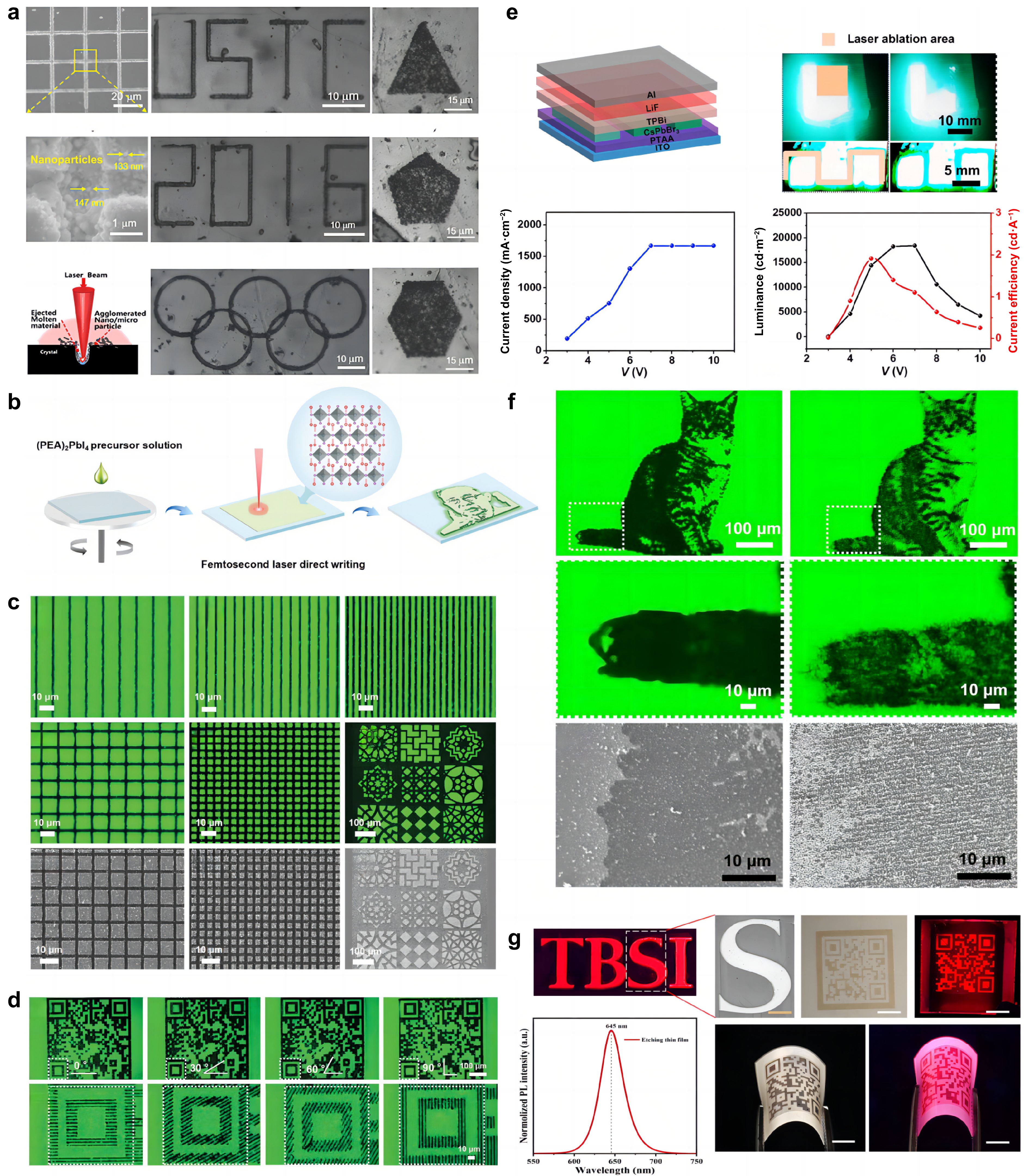
Fig. 6 Study of various patterned structures. a Various designed microstructures from nanoparticles and microlines to 2D micropatterns. Reproduced with permission97. Copyright 2017, IEEE Photonics Journal. b Process flow diagram for the FsLDW fabrication of patterned 2D perovskite films. c Fluorescence and scanning electron microscopy (SEM) images of microlines of 2D perovskite films with different widths. d Schematic of QR code anti-counterfeiting principle. Reproduced with permission98. Copyright 2022, Wiley-VCH. e Light-emitting diode emission characteristics based on ablated perovskite thin films. Reproduced with permission99. Copyright 2022, American Chemical Society. f Fluorescence cat image, high magnification fluorescence image, and SEM image of patterned CsPbBr3 film. Reproduced with permission100. Copyright 2023, The Royal Society of Chemistry. g Fluorescence patterned perovskite produced by laser ablation on various substrates. Reproduced with permission101. Copyright 2023, The Royal Society of Chemistry.
In addition to their applications in displays, image sensing, and fluorescence anti-counterfeiting, perovskites show immense potential in the semiconductor field owing to their long carrier diffusion length, defect tolerance, and high PLQY102,103. The development of perovskite patterning technologies is essential in fields such as integrated circuits and solar cells. However, the preparation of high-quality, high-density, high-resolution, and high-transparency perovskite patterns remains a challenge104 for the fabrication of integrated circuits and solar cells. Recent research has shown that femtosecond laser ablation is an effective perovskite-patterning technique that can produce high-quality, high-resolution perovskite structural patterns. In 2020, Zhizhchenko et al.105 successfully created high-quality and repeatable subwavelength resonant nanostructures, nanohole arrays, QR codes, and perovskite nanowires with a width of 500 nm using femtosecond laser ablation with optimized pulse sequences and specifically designed beam profiles. Zhao et al.106 utilized femtosecond laser direct-writing technology to create a semitransparent perovskite solar cell (ST-PSC), which achieved a conversion efficiency of 9.1% and an average visible transmittance of 37.7%, in the fabrication of solar cells. The creation of light-passing channels with microstructures on the absorber layer could increase the transparency of PSCs107–110. Compared with other technologies, this approach is simpler and allows the customization of patterns to meet the requirements of aesthetic architectural design. These studies highlighted the advantages and potential of femtosecond laser ablation for the production of high-quality, high-density, high-resolution, and high-transparency perovskite patterns. Future research can explore the application of this technology to create larger perovskite patterns and higher fabrication efficiencies through systematic experiments to promote its widespread application in various fields, including integrated circuits and solar cells.
Accomplishing high-quality and high-precision patterning of halide perovskite films is crucial for image sensors and displays57,111. To obtain high-resolution perovskite 2D patterns, Liang et al. conducted extensive experimental research. In 2022, the researchers first investigated patterning of high-humidity-stable perovskites and developed a facile FsLDW method to fabricate arbitrary 2D perovskite films with clear contours and uniform fluorescence characteristics; a high resolution of 1.78 µm line width98 was accomplished. Fig. 6b illustrates the process of fabricating the patterned 2D perovskite films using a femtosecond laser, and Fig. 6c displays the fabricated pattern. In addition, Liang et al. studied a fluorescent anti-counterfeiting label (2D code embedded with microlines) based on the high humidity stability of the 2D perovskite films, in which anti-counterfeiting was accomplished by adjusting the angle of the microlines, as shown in Fig. 6d. To verify the stability of the pattern, PL spectroscopy tests were conducted on the patterned 2D perovskite films at different relative humidity levels (from 43% to 96%). The original intensity was defined as the PL intensity measured in cleanroom air at 15% relative humidity (RH). Owing to the stability of the 2D perovskite in high humidity, the PL curves exhibited at 43% RH were almost identical to the original and maintained approximately 60% of the original intensity at the high RH of 75%. Additionally, patterned QR codes based on 2D perovskite films with relative humidities ranging from 43% to 96% were recognizable by smartphones, demonstrating stable anti-counterfeiting functionality in high-humidity environments. These results demonstrate that fluorescent anti-counterfeiting labels fabricated using FsLDW can be arbitrarily designed and exhibit high humidity stability. In the same year, Liang et al.99 successfully applied the lamination-assisted femtosecond laser ablation (LA-FsLA) technique to fabricate high-quality and high-precision patterned CsPbBr3 films that exhibited strong fluorescence intensity. Using a sandwich structure (glass/CsPbBr3/glass) prevented the impact of debris generated during processing on the unprocessed areas, thereby, markedly improving the quality of the pattern. The ablation efficiency of the perovskite film was maximized by adjusting the femtosecond-laser fluence and scanning speed. Furthermore, the researchers constructed an LED based on an ablated perovskite film that exhibited excellent emission characteristics. In Fig. 6e, the LEDs demonstrate high luminance and efficiency, with maximum values reaching 18,390 cd m-2 and 1.9 cd A-1, respectively. These results underscore the potential of the LA-FsLA technique to enhance the performance of perovskite optoelectronic devices. This technology facilitates future applications in anti-counterfeiting devices, displays, and image sensors.
To meet the demand for the miniaturization and integration of photonics and optoelectronic devices, Liang et al.100 used a femtosecond laser to adjust the focus and achieved a high resolution of up to 1/10 that of the diffraction limit ratio when burning candle fluorescent films. During fabrication, different brushes were used to process different areas of the pattern to create a layered image. The correct candle-burning focal point was established by simulating the intensity distribution of the light-field morphology at different focal depths using optical field simulation software. The SEM image of the femtosecond laser single-pulse ablated lattice confirmed that the resolution of this technique far exceeded the diffraction limit of the femtosecond laser regulatory focus ablation (FsLRFA) patterning technique. In addition, the PL spectra before and after burning the candle were the same, indicating that femtosecond laser burning did not affect the fluorescence characteristics of the perovskite. As shown in Fig. 6f, the method used by Liang et al. produced images (right) that were more vivid and had clearer edges and more uniform fluorescence characteristics than those produced using traditional methods (left). This technology, which displays nano-scale resolution and freeform patterning capability, has potential for highly integrated applications based on fluorescent materials. In the same year, Liu et al.101 fabricated perovskite materials with a high PLQY of up to 91% and high stability and achieved a complex pattern display on rigid and flexible substrates using a femtosecond laser (Fig. 6g). For example, in a QR code, bright red fluorescence is displayed under UV light, thereby enabling encryption and decryption through on/off switching of UV lamps in anti-counterfeiting applications. This versatile display technology for perovskite materials promotes their application in novel directions.
-
The recent introduction of 2D perovskite flat lenses has sparked a trend toward low-cost and scalable multidisciplinary applications112. Optical microscopy has notable application value in fields such as materials science, physics, biology, and microelectronics113–115. Optical materials with a high refractive index, strong absorption, and tunable optical properties are key for manufacturing controllable flat lenses to manipulate light amplitude and phase116,117. A simple ion-exchange process can effectively adjust the optical constants of 2D perovskite materials, providing a foundation for manufacturing optical lenses with special properties. Cherepakhin et al.118 synthesized advanced binary micro-optical components based on CsPbBr3 perovskite microcrystals via high-throughput manufacturing using direct femtosecond-laser projection lithography, and accomplished nanoscale focusing and advanced the generation of optical vortex beams. The researchers studied the focusing performance of perovskite micro-optical devices by illuminating their surfaces with a 515 nm central wavelength (CW) collimated beam. In addition, a calibrated charge-coupled device (CCD) camera was used to generate the intensity distributions in the corresponding focal plane reflections. High-quality reflective binary micro-optical elements, such as Fresnel zone plates, binary spiral microaxicons, and binary fork gratings were also manufactured. These components and holograms can be directly imprinted using nondestructive and phase-correlated laser technologies, as demonstrated by this technique. Fig. 7a shows a schematic of the femtosecond laser projection lithography setup, illustrating the fabrication process of various micro-optical elements. The corresponding focal-plane intensity distribution at an excitation wavelength of 515 nm demonstrates the focusing performance of the printed 2D perovskite micro-optics.
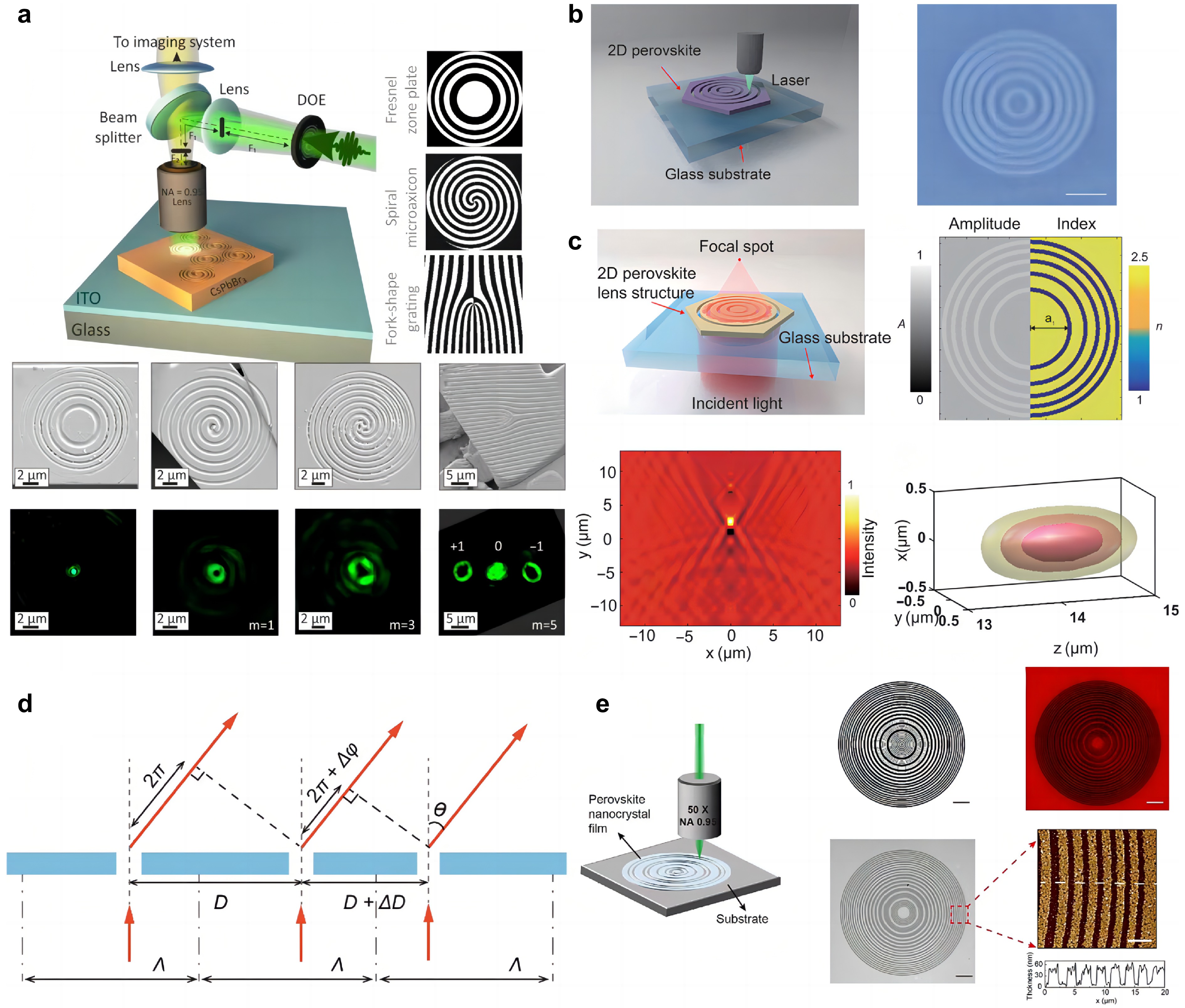
Fig. 7 Manufacturing process and working principle of lenses. a Schematic diagram of femtosecond laser projection lithography system with various micro-optical components. Reproduced with permission118. Copyright 2021, IOP Publishing. b Schematic illustration of direct laser writing for fabrication of 2D perovskite lens and optical image of 2D perovskite planar lens. c Refractive index distribution of the lens and corresponding amplitude modulation. Reproduced with permission119. Copyright 2020, WILEY-VCH. d Schematic illustration of the detour phase modulation rule for arbitrary wavefront shaping. e Direct laser writing of perovskite nanocrystal ultrathin planar (PUP) lens on perovskite film. Reproduced with permission120. Copyright 2022, Optica Publishing Group.
Optical phase modulation has been widely used in the fields of optical communication121, optical signal processing122, microwave signal processing123, and other related areas. As an important photonic functionality, optical phase modulation has been demonstrated using perovskite substrates and laser inscription of complex refractive index engineering. Wang et al.119 fabricated ultrathin flat lenses based on 2D perovskite nanosheets using femtosecond laser writing (Fig. 7b). The fabricated lenses can effectively control the amplitude and phase of the incident light using simple ion substitution or quantum size confinement; thus, light can be focused on 3D focal spots with a subwavelength resolution in the range between 0.5–0.9 λ. Fig. 7c shows the refractive-index distribution and corresponding amplitude modulation of the lens. Wang et al. demonstrated that amplitude modulation is the primary contributor to coherent interference in ultrathin 2D perovskite lenses, whereas the focusing principle of thick 2D perovskite planar lenses (e.g., >100 nm) relies on the synergistic effect of both amplitude and phase modulation. Subsequently, a precise design approach for 2D perovskite flat lenses based on the Rayleigh–Sommerfeld (RS) diffraction theory was developed and perovskite lenses can be designed with consistent parameters without the need for near-axis constraints. However, Yang et al.120 discovered that the design developed by Wang was limited to small apertures less than 10 µm, and the width of the edge region in the waveband design became too narrow, making it difficult to accomplish through direct laser writing. Additionally, precise control of the modulation of the electronic field of a lens through amplitude and phase modulations was difficult. Therefore, Yang et al. designed high-performance perovskite nanocrystal ultrathin planar (PUP) lenses with a diameter of 150 μm, working wavelength of 532 nm, and focal length of 310 μm based on the detour phase method. The researchers proposed a theoretical model to study the focal field based on the scalar Fresnel diffraction theory, which agreed well with the experimental results. The principle governing the modulation of the designed lens phase is shown in Fig. 7d. Unlike in the waveplate lens, in the detour phase method, the linewidth can be flexibly selected and is independent of the focal length. PUP lenses were manufactured using a direct femtosecond laser writing process, as shown in Fig. 7e. The desired lens profile was produced in a single-step writing process without back-and-forth optimization, demonstrating the significant benefits of the one-step mask-free direct laser writing technique. This technology simplifies the design and manufacture of lenses. Yang et al. observed high-performance 3D focal points, studied the fabrication process using different parameters, and demonstrated the imaging capabilities of the PUP lenses. The low-cost in-situ preparation of perovskite materials and use of direct laser writing to manufacture high-performance PUP lenses should facilitate numerous applications and miniaturized on-chip devices in the near future.
-
Perovskite single-crystal microdisk lasers play an important role in advanced nanophotonic designs owing to their high-gain and wavelength tunability124. Currently, solution-processed, high-gain, and wavelength-tunable perovskite single-crystal microdisk lasers are potential coherent light sources for advanced nanophotonic design124 and ultrafast information-processing photonic integrated circuits125. Among them, perovskite microdisks are manufactured based on high-quality thermally co-evaporated FAPbI3 thin films, which have a small grain size, controllable thickness, and smooth surface. In 2019, Zhizhchenko et al.126 used a ring-shaped femtosecond laser beam to burn perovskite thin films onto glass and manufactured microdisks. The thickness of the microdisk is 760 nm, and the diameter ranges from 2–9 μm. The laser characteristics of the different microdisks are shown in Fig. 8a. Statistical analysis revealed that more than half of the microdisks exhibited single-mode lasing, with a random deviation of approximately 7 nm from the central laser wavelength of 787 nm. Moreover, microdisks with varying perovskite compositions demonstrated similar single-mode states. The single-mode perovskite miniaturized laser manufactured using this method can operate over a wide spectral range of 550–800 nm at room temperature, and its Q factor is as high as 5500. A neatly arranged microdisk array processed using this method is shown in Fig. 8b. This femtosecond laser processing method offers a faster, more cost-effective, and entirely controllable approach for manufacturing conventional centimeter-sized perovskite microlaser arrays. In the same year, Ivan et al.127 developed a new method for manufacturing perovskite microdisks using a direct femtosecond pulse collision-patterned laser on a MAPbI3 thin film; the method of manufacturing perovskite microlasers was faster, more controllable, scalable, and cost-effective. Simultaneously, laser printing conditions were optimized to produce high-quality perovskite microdisks with smooth sidewalls and low thermal damage to the internal materials. Fig. 8c shows the two perovskite microdisks produced under quasi-continuous-wave exposure (left) and burst-mode melting (right). Burst-mode printing produces a smoother microdisk sidewall and does not reduce the luminescence properties of the perovskite material in the microdisk, which is more conducive to the observation of laser generation.
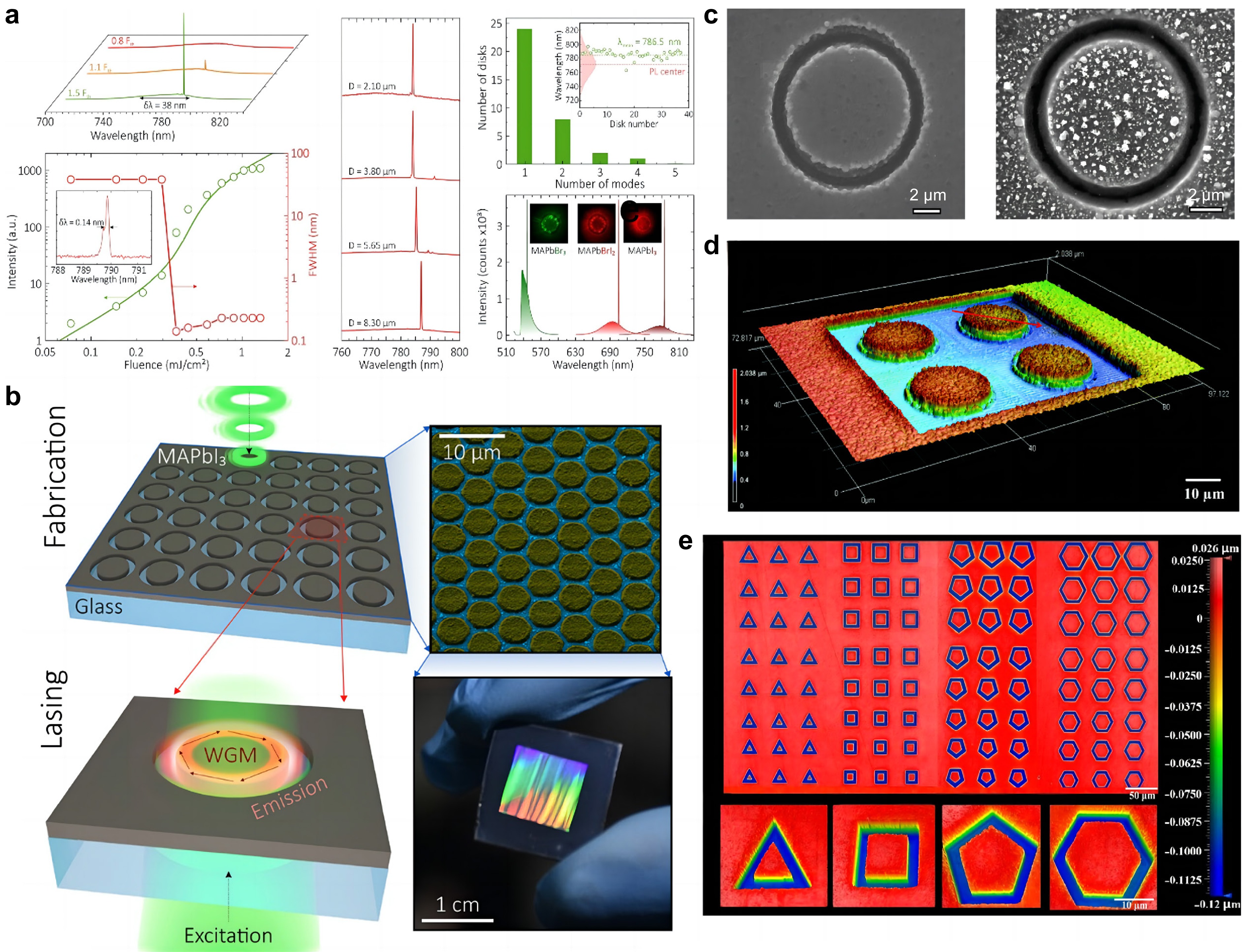
Fig. 8 Fabrication performance and types of perovskite microdisk. a Laser characteristics of different perovskite microdisks. b Fabrication of large-scale arrays of perovskite microlasers and their photoexcitation. Right panel: close-up false-color scanning electron microscopy (SEM) image (top) and photograph of a 1 × 1 cm2 array of perovskite microlasers126. Copyright 2019, American Chemical Society. c SEM image of perovskite microdisk127. Copyright 2019, IOP Publishing. d 3D laser scanning confocal microscopy image131. Copyright 2020, The Royal Society of Chemistry. e Patterned FAPbI3 microcavities, including triangular, square, pentagonal, and hexagonal132. Copyright 2021, American Chemical Society.
In 2014, rapid development of perovskite lasers occurred128 owing to the discovery of spontaneous emissions from perovskite thin films. Manufacturing methods for perovskite lasers can be divided into two categories: bottom-up and top-down129. However, microlasers obtained using the bottom-up method are more susceptible to manufacturing conditions, whereas the top-down method has advantages such as large-area manufacturing and high controllability130. A simple and effective method for producing reproducible perovskite microcavities is essential for the mass production of reliable halide lead-perovskite lasers. Tian et al.131 used the top-down method to fabricate formamidinium lead iodide (FAPbI3) perovskite microdisks to investigate the influence of the size of the microdisk (diameter and thickness) on laser performance, and accomplished an ultra-low threshold perovskite microdisk laser of approximately 3 μJ cm−2. Fig. 8d shows a confocal microscopy image of a perovskite microdisk. This manufacturing method is highly reproducible and controllable, making it suitable for mass production. Simultaneously, Tian et al. fabricated perovskite microdisks with different diameters and thicknesses and discovered that the laser performance (i.e., mode spacing and pump threshold) depends greatly on the microdisk diameter but the thickness does not have much impact.
The cavities of microlasers can be designed in various shapes, such as spheres, microdisks, and micro-rings, and these shapes can produce high Q factors126. Interestingly, microlasers based on regularly shaped polygonal microresonators have shown superior mode characteristics compared with that of circular microcavities133–135. However, a method for mass-producing perovskite polygonal microlasers is currently lacking, posing a significant challenge for the further development of the applications of this type of laser. High-quality polygonal perovskite microcavities with a low pump threshold and narrow FWHM have broad application prospects in the field of optoelectronic integration. Tian et al.132 improved a microcavity based on a microdisk and successfully prepared triangular, square, pentagonal, and hexagonal FAPbI3 polygonal microcavities. The microcavity boundary and smooth surface are not significantly damaged, and the surface roughness is low (Fig. 8e). High-performance microcavity lasers require suitable optical resonators, regular shapes, and low roughness136. FAPbI3 thin films have high crystallinity, high surface smoothness, and ideal polygonal shapes, ensuring they are suited to high-quality whispering gallery mode (WGM) resonator applications. In addition, the microcavity size and shape influence the WGM laser performance. The hexagonal FAPbI3 microcavity exhibits the lowest pump threshold (approximately 4.0 μJ cm−2) and narrowest FWHM (approximately 0.62 nm). The laser threshold and FWHM decrease the order of the polygonal shape of the microcavity.
Recently, Liang et al.137,138 proposed a novel technique called femtosecond-laser-induced forward transmission (FsLIFT), which involves focusing a femtosecond laser on the interface between the PQD film and carrier substrate, resulting in plasma generation and expansion through the nonlinear absorption of the PQD films. Subsequently, PQDs within the laser-irradiated area are explosively transferred to the receiving substrate. Transfer, deposition, patterning, and alignment were integrated in a single step (Fig. 9a). Precisely aligning the positions of R/G/B subpixels within a pixel poses a challenge for PQD displays. Liang et al. successfully obtained a fluorescence image of a full-color PQD-micropatterned butterfly using the FsLIFT technique (Fig. 9b), and successfully prepared full-color PQD arrays with various sizes (50, 20, and 2 μm), which is crucial for display applications. Furthermore, the researchers compared the thermally annealed and laser-printed perovskite films. Fig. 9c shows atomic force microscopy (AFM), fluorescence, and SEM images of both types of films. Compared with thermally annealed CsPbBr3 films, the laser-printed films demonstrated higher crystalline quality, stronger fluorescence, and surface roughness, meeting the requirements of optoelectronic device applications. These findings highlight the significant facilitation for the application of PQDs in areas such as high-resolution displays and image sensing.
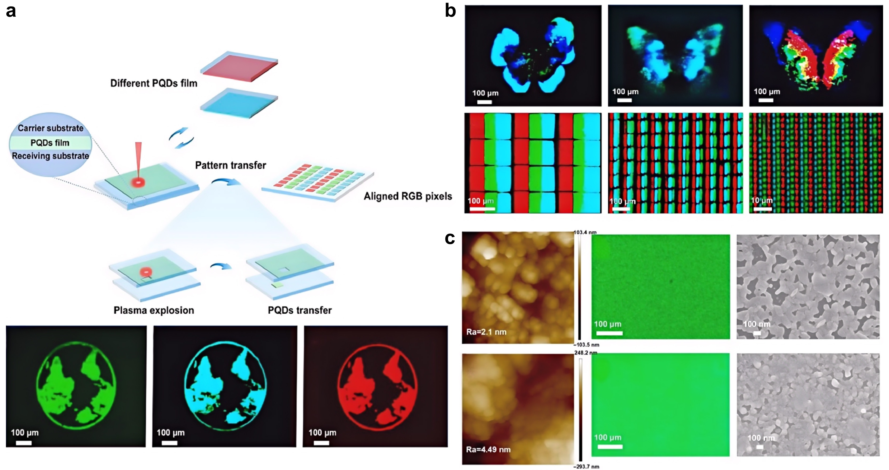
Fig. 9 Femtosecond laser-induced forward transmission technology. a Principle of femtosecond laser-induced forward transmission technology and schematic diagram of the prepared R/G/B PQD array. b Fluorescence image of full-color PQD micropattern. The resolution is 50 μm, 20 μm, and 2 μm from left to right138. Copyright 2023, American Chemical Society. c Atomic fluorescence microscopy, fluorescence, and scanning electron microscopy images of CsPbBr3 film printed by thermal annealing (top) and femtosecond laser printing (bottom)137. Copyright 2023, American Chemical Society.
-
The unique crystal structure and excellent performance of perovskites ensure they are promising materials for numerous optical and optoelectronic applications. As femtosecond laser technology continues to develop with increasingly shorter pulse widths and higher peak powers, it has become a powerful tool for processing complex 3D structures and promoting progress in fundamental research fields, such as physics, chemistry, biology, and medical engineering. This paper introduces two aspects of femtosecond-laser-induced perovskite precipitation and processing, emphasizing the advantages of nonlinear, high-precision, high-efficiency, and material adaptability of femtosecond lasers in perovskite material processing. Femtosecond laser processing is not only limited to the micromachining of perovskite materials but also induces the precipitation of perovskite materials inside glass, which is crucial for improving the stability, thereby promoting their applications and development in various fields.
Perovskite materials can be prepared using various methods such as high-temperature solid-state synthesis, sol-gel synthesis, and hydrothermal synthesis. However, these methods all prepare perovskite materials in air, making it difficult to avoid the influence of temperature and humidity on the performance of the perovskite material. Femtosecond laser-induced micro-and NCs in transparent materials, combined with annealing processes, can achieve selective removal and regeneration of perovskite materials, providing potential for their applications in anti-counterfeiting and information storage fields. Nevertheless, the current femtosecond laser manufacturing method for perovskites still needs to be further optimized and improved to achieve higher preparation efficiency and better performance.
Femtosecond laser processing of perovskite materials includes PQDs, nanowires, and 2D patterning, which illustrate the non-linear, high-precision, high-efficiency processing ability, and superior material adaptability of the femtosecond laser. They have noteworthy applications in optoelectronic detection, information storage, biomedicine, and other optoelectronic devices. Perovskite materials may be uniquely processed and prepared by adjusting the femtosecond laser power, exposure time, and scanning speed. However, there is still much room for improvement in femtosecond laser micro-nano processing of perovskite materials. For example, research can be performed on how changing the composition and surface polymer coating of perovskite materials can affect the stability and exciton properties of halide perovskite nanostructures, to explore light storage that can retain information for an extended duration. Femtosecond laser technology has broad prospects in perovskite material processing. Future research should focus on the characteristics of perovskite materials and synergistic interaction with other materials, thereby leading to greater innovation.
-
This work was financially supported by the Guangdong Basic and Applied Basic Research Foundation (2022A1515011951, 2023A1515012977, 2024A1515010109), the National Natural Science Foundation of China (62375056), and the Science and Technology Program of Guangzhou (202201010182).
Advances in femtosecond laser synthesis and micromachining of halide perovskites
- Light: Advanced Manufacturing 5, Article number: (2024)
- Received: 19 December 2023
- Revised: 15 June 2024
- Accepted: 06 July 2024 Published online: 15 July 2024
doi: https://doi.org/10.37188/lam.2024.035
Abstract: Perovskite materials have become a popular research topic because of their unique optical and electrical properties, that enable extensive applications in information storage, lasers, anti-counterfeiting, and planar lenses. However, the success of the application depends on accomplishing high-precision and high-quality perovskite patterning technology. Numerous methods have been proposed for perovskite production, including, a femtosecond laser with an ultrashort pulse width and ultrahigh peak power with unique advantages such as high precision and efficiency, nonlinearity, and excellent material adaptability in perovskite material processing. Furthermore, femtosecond lasers can induce precipitation of perovskite inside glass/crystals, which markedly enhances the stability of perovskite materials and promotes their application and development in various fields. This review introduces perovskite precipitation and processing via femtosecond lasers. The methods involved and advantages of femtosecond-laser-induced perovskite precipitation and patterning are systematically summarized. The review also provides an outlook for further optimization and improvement of femtosecond laser preparation and processing methods for perovskites, which may offer significant support for future research and applications of perovskite materials.
Rights and permissions
Open Access This article is licensed under a Creative Commons Attribution 4.0 International License, which permits use, sharing, adaptation, distribution and reproduction in any medium or format, as long as you give appropriate credit to the original author(s) and the source, provide a link to the Creative Commons license, and indicate if changes were made. The images or other third party material in this article are included in the article′s Creative Commons license, unless indicated otherwise in a credit line to the material. If material is not included in the article′s Creative Commons license and your intended use is not permitted by statutory regulation or exceeds the permitted use, you will need to obtain permission directly from the copyright holder. To view a copy of this license, visit http://creativecommons.org/licenses/by/4.0/.

 DownLoad: