


-
Future optical communication and signal processing systems will require high-volume optical links, wherein photonic integrated devices play a key role1. Silicon (Si) photonics is currently among the most advanced techniques for realising low-cost photonic integrated circuits (PIC)2,3. This technology is primarily based on its complementary metal-oxide-semiconductor (CMOS) compatibility and the accessibility of high-quality and low-cost silicon-on-insulator (SOI) wafers. The high refractive index of Si waveguides offers strong optical confinement, which facilitates a decrease in the size of photonic integrated circuits to the submicron range4. However, despite their enormous potential, there remain basic restraints on light modulation in SOI waveguides. The absence of a linear electro-optical (EO) coefficient is challenging because of the crystal structure of Si5. Many methods have been proposed to overcome these limitations. The most commonly used method involves facilitating the Pockels effect in other materials6,7, through which EO modulation permits the realisation of excellent modulation performance without additional losses.
Materials with considerable Pockels coefficients integrated on SOI platform have emerged as a prospective path to the achievement of high-efficiency EO modulation8,9. Ferroelectric materials have been used for modulation owing to their excellent EO coefficients, thermal and temporal stability, and excellent optical transparency10–15. The most common ferroelectric oxide is lithium niobate (LiNbO3, LN), and is widely used in communication systems16–19. Among the most commonly used approaches involves the use of LiNbO3 on insulator (LNOI) thin film17,20–24 and hybrid integrated on SOI platform, which combines the favourable properties of LiNbO3 crystal and achieves compact high-index-contrast waveguides. However, the relatively small Pockels coefficient (r33 = 31 pm/V) of LiNbO3 limits the performance of modulators to a certain extent, resulting in large device footprints, typically in the millimetre-to-centimetre range. Therefore, to further decrease the footprint of the modulator and increase the efficiency, materials with larger EO coefficients than those of LiNbO3 are of great interest, which would decrease the footprint of the device and reduce the velocity mismatch between the optical and electrical waves for large bandwidths. Barium titanate (BaTiO3, BTO)9, is known for its high Pockels coefficient among various ferroelectric oxides, which is several times higher than that for LiNbO39,25,26, and has attracted considerable interest in the study of EO modulation in recent years26–29. Recently, a high data rate BTO modulator supporting a transmission rate of 200 Gb/s has been demonstrated30, which renders BTO technology particularly attractive. However, a potential problem during the integration of materials on SOI is the lattice mismatch between the ferroelectric film and Si substrate, which prevents the ferroelectric film from being deposited directly on the Si. Despite numerous attempts, the integration of Si and high-quality thin films can only be realised by sophisticated and expensive layer-bonding methods16, which renders integration with standard CMOS technology difficult. Various studies have been conducted to develop hybrid BTO/Si integration technologies. Several researchers have succeeded in this integration by growing strontium titanate (SrTiO3, STO) as a buffer layer between the ferroelectric layer and Si using molecular beam epitaxy (MBE)31–35, thereby providing a novel method for the research of high-performance hybrid Si BTO modulators36. However, typical defects are found in the BTO layer on a Si substrate, and the thickness of BTO is typically up to 150 nm with a slow growth rate32,37. Therefore, the development of stripping and transfer technologies for oxide films is a key step in the manufacture of high-quality epitaxial oxide films. Recently, an environmentally friendly and nondestructive method was proposed to generate freestanding epitaxially grown inorganic films by dissolving water-soluble Sr3Al2O6 (SAO) layers. Free-standing films can be successfully transferred onto SOI wafers38–42. Compared to the previously mentioned technique of growing STO as a buffer layer between the BTO and Si substrate, the transfer method can improve the effective EO coefficient by changing the rotation angle of the BTO layer. Consequently, we can obtain free-standing epitaxial BTO films with remaining excellent ferroelectricity36,43,44 and flexibility45,46 on top of SOI waveguides. By exploiting the evanescent-coupling BTO film and SOI waveguide, EO modulation can be realised47.
This study demonstrated EO modulation using the hybrid integration of BTO on a Si Mach-Zehnder interferometer (MZI) enabled by the target transfer method. We first optimised the thicknesses and rotation angles of the BTO films to enhance the EO modulation in the SOI waveguide. Furthermore, as a proof of principle, we transferred the BTO film onto Si MZIs and demonstrated phase modulation via BTO films through evanescent coupling. The proposed device exhibited a large modulation efficiency with $ {\text{V}}_{\text{π}} $L as low as 1.67 V·cm. The results of this study are expected to pave the way for hybrid integration of BTO modulators on SOI platforms.
-
The proposed device comprised SOI waveguides, a BTO layer, and metal contacts. The Si waveguide was buried in an oxide layer on a Si substrate. The thickness of the oxide buffer layer t2 was 2 μm and chemical mechanical polishing (CMP) was used to flatten the surface on top of the Si waveguide, leaving a thin layer of SiO2 t1 = 5 nm on top. The width of the Si waveguide WSi, was 500 nm, and the thickness tSi, was 220 nm. The SOI waveguide chip was fabricated using a CMOS foundry (CUMEC) (Fig. S1).
As shown in Fig. 1a, a BTO film was placed on top of a Si waveguide. The thickness of the BTO layer is among the most crucial factors affecting the Pockels effect. Therefore, the thickness tBTO was optimised to 150 nm to ensure high-quality epitaxial BTO films and a strong Pockels effect. The BTO thin film was transferred onto the target substrate by dissolving the SAO layer in water. Thus, the ferroelectricity and quality of the BTO film were maintained simultaneously, and the BTO layer could be used directly without etching.
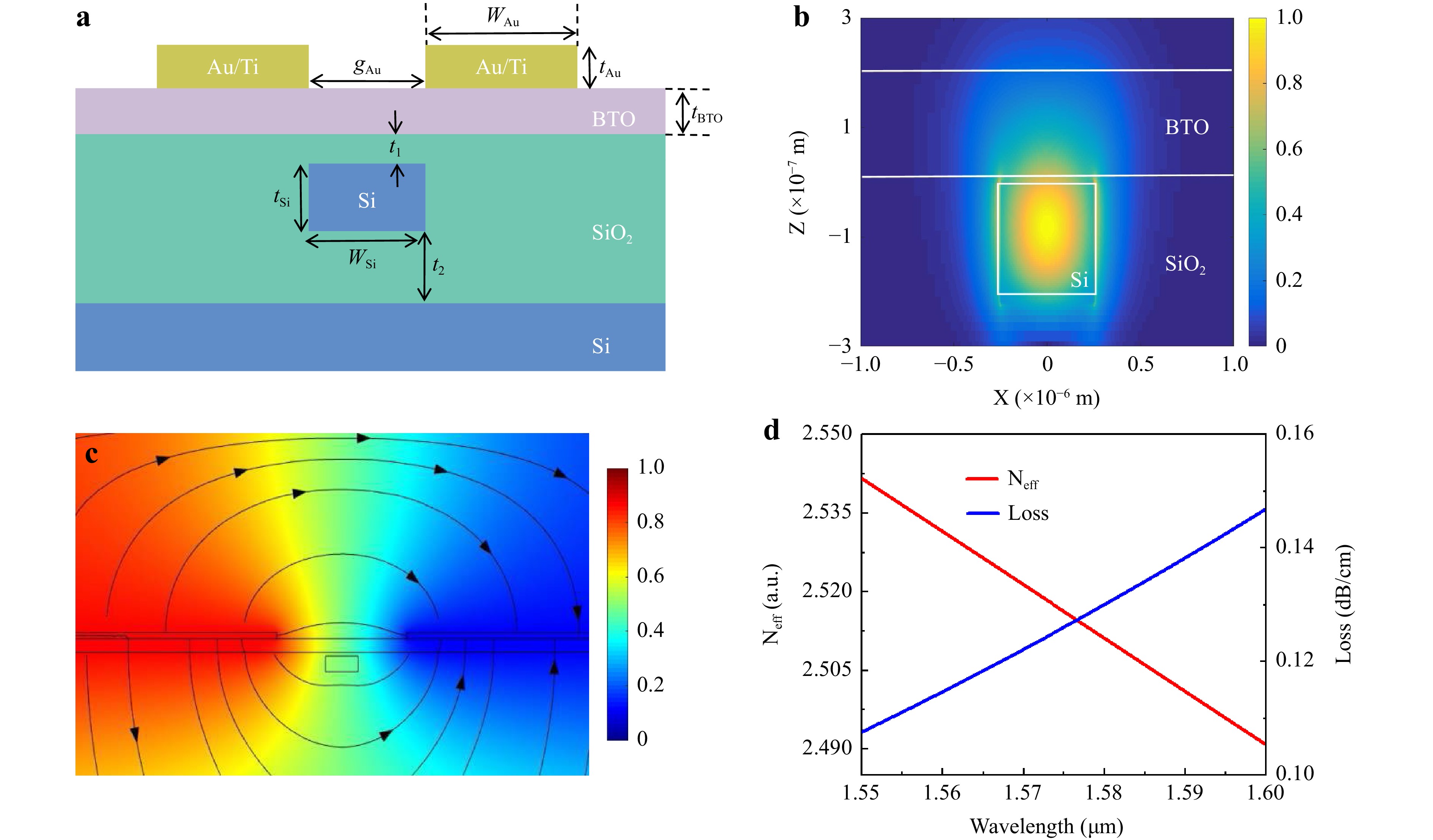
Fig. 1 EO modulation using hybrid integration of BTO on a Si MZI. a Cross-sectional view of the BTO on Si-based waveguide modulator. The optical waveguide is parallel to the (100)-oriented BTO. The metal contacts are deposited close to the waveguide. b Simulated mode profiles of the photonic TE modes. The colours indicate the electric field strength, ranging from blue (low) to red (high). c Cross-sectional schematic of the EO modulators with electric field distribution, where the lines in the figure are electric field lines and the arrows indicate the direction with a DC bias voltage of approximately 10V. d Finite-difference eigenmode (FDE) characterization of the effective refractive index and optical loss as a function of wavelength.
The metal contacts were formed by depositing 5 nm of titanium and 80 nm of Au on a BTO layer. Through the application of voltages across the two contacts, an electric field was formed and the BTO layer was polarised, resulting in a difference in the refractive index of the ferroelectric films. The active length of the MZI EO modulator was set to 286 μm. The light wave in the waveguide was evanescently coupled with the thin films and was subjected to a phase change. We set the distance of the two contacts gAu as 4 μm to reduce the absorption loss from metal contacts and maintain a small gap for a stronger electric field between the contacts. As shown in Fig. 1b, the significant difference in the refractive indices of Si and SiO2 $ ({\text{n}}_{\text{Si}}={3.47},\;{\text{n}}_{\rm{SiO_2}}= 1.46 $) in the SOI structure facilitated the confinement of the optical field in the Si waveguide. Compared to the bottom oxide layer, the higher refractive index of BTO (nBTO = 2.38) pushed the optical field towards the BTO layer, further promoting evanescent coupling. Owing to the high Pockels effect of BTO, voltages must be applied to achieve relatively large variations in the effective refractive index. Fig. 1c shows the modulated electric field distribution at 10 V, which is the DC bias voltage. The DC bias field is critical for the complete polarisation of the BTO film; therefore, the voltages in this study represent DC voltages. To illustrate the dependence of modulation on the DC bias field, we tested the output waveforms of the EO modulators at different bias voltages. The effective refractive index and optical loss of the EO modulators at the centre wavelength (approximately 1550 nm) were calculated using FDE, shown in Fig. 1d. As evident, the transmission loss of the structure was 0.13 dB/cm at a wavelength of 1.55 μm. This value was obtained by simulating the imaginary part of the effective refractive index. Based on the values of the electrode gap, light field, and electric field, we calculated the EO overlap integral $ \mathrm{\Gamma } $ as 0.58. Simulations and experimental validation3 indicated that the EO integral Γ increased significantly with the thickness of the BTO film. The thickness of the BTO film also affected the effective Pockels coefficient. Therefore, the thickness of the film must be optimised. The goal of our design dictated a considerable overlap between the driving electric and optical fields.
-
The free-standing single-crystalline BTO film was fabricated based on the epitaxial growth of a BTO/SAO/STO heterostructure (see Methods). BTO/SAO heterostructures were deposited onto the STO layer via pulsed laser deposition (PLD). We used a reliable photoresist transfer method with a positive photoresist-type AZ5214. This photoresist can be completely dissolved in acetone, and is therefore suitable for film transfer. During the transfer process, the photoresist was spin coated onto the sample surface to cover the entire BTO surface. The sample was heated at 115 °C for 25 min to fully harden the photoresist. It was then placed in deionised water. Once the SAO water-soluble sacrificial layer was completely dissolved, the BTO film was transferred onto the target SOI substrate. Compared with other film transfer methods, precise control of the rotation angle between the sample and the substrate was enabled. In addition, fewer residues on the film surface are beneficial. Therefore, the flexible photoresist transfer method is more appropriate for our experiments. In this process, we focused on controlling the surface roughness of the BTO samples (Fig. S2). The average roughness can be controlled within a certain range and selected by measuring the atomic force microscopy (AFM) images of the surface of a 150 nm thick BTO film. In this case, the film surface was relatively smooth, with an average roughness of 1.32 nm (Fig. S3). Next, the single-crystal BTO film was freed from the STO substrate by dissolving the sacrificial SAO layer in water. The transfer process of the BTO film is schematically illustrated in Fig. 2a, c.
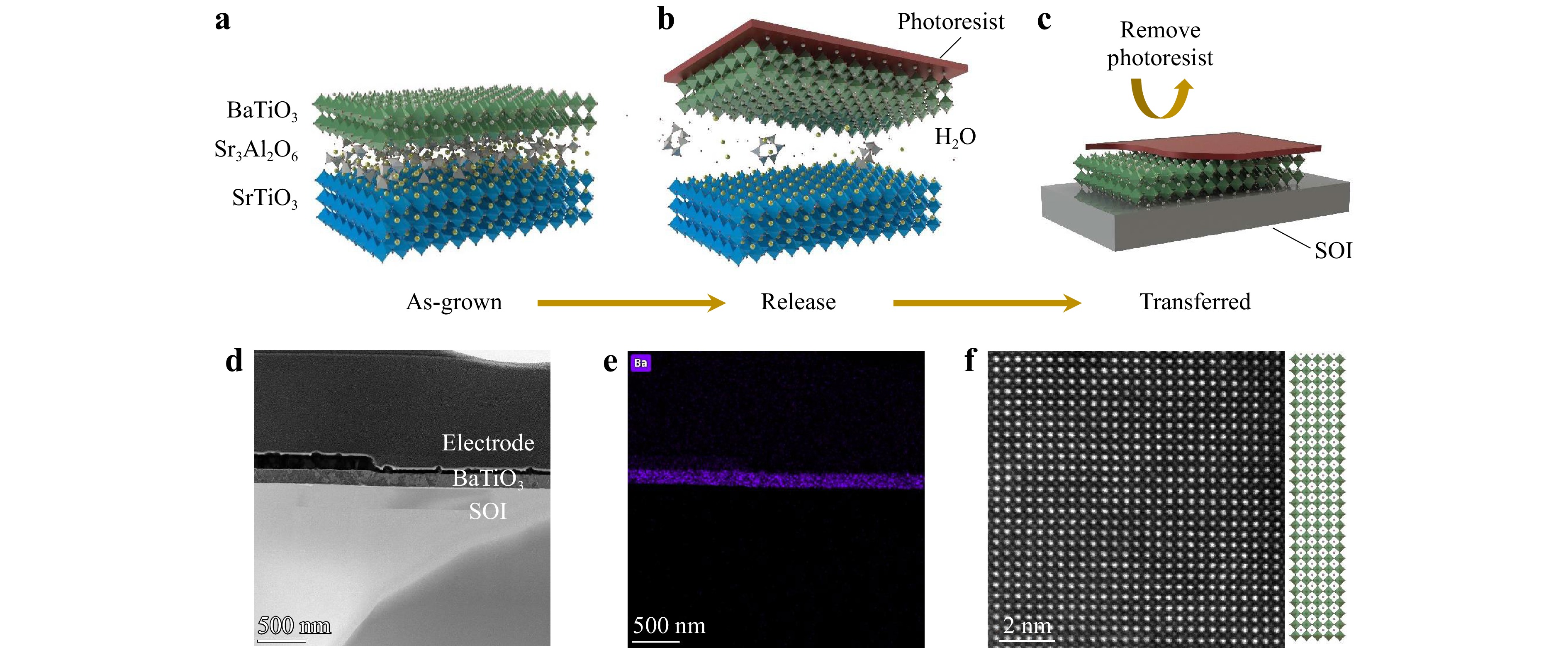
Fig. 2 a–c Schematics of single crystal BTO peeling-off and transfer process from STO to the SOI substrate. d Cross-sectional transmission electron microscopy (TEM) image of a contact/BTO/SOI heterostructure. e EDS element mapping of Ba element. f Atomic resolution STEM image of BTO layer.
During this process, the photoresist supporting layer on the surface of the epitaxial BTO film can be removed entirely using an organic solvent. After the film was transferred to the target substrate, its orientation relative to the substrate was freely adjusted until the sample was completely dry (Fig. S4). A cross-sectional transmission electron microscopy (TEM) image of the contact/BTO/SOI heterostructure is shown in Fig. 2d, with a metal contact layer on top, followed by the BTO and SOI layers. The thickness of the BTO film was estimated to be 150 nm, and the interface between the BTO and SOI layers was sharp and distinct. Energy dispersive X-ray spectroscopy (EDS) element mapping revealed a homogeneous distribution of Ba, as shown in Fig. 2e. Fig. 2f shows an atomic-resolution cross-sectional scanning transmission electron microscopy (STEM) image of the BTO layer, demonstrating the atomic homogeneity and lattice structures that matched well with the corresponding models of BTO.
Plane-view SEM images of the contact/BTO/SOI heterostructure are shown in Fig. 3a, b. To examine the ferroelectricity of the transferred BTO layer, Fig. 3c exhibits the response curves observed under a microscope when piezoelectricity was applied out-of-plane to the transferred BTO film. Further, the region where +9 V positive bias was applied to the film was polarised upward, whereas the negative bias of -9 V was polarised downward in this figure. The crystallinity of the BTO film on STO/SAO and SOI was tested using X-ray diffraction (XRD) (Fig. 3d), where the blue line indicates that only the (00l) diffraction peaks from BTO, SAO, and STO were detected with growth in the BTO/SAO/STO. The XRD profile of the STO/SAO/BTO film after transfer is indicated by the red line. A comparison of the images before and after the transfer demonstrated that the properties of the BTO films changed owing to stress relief before and after the transfer. Moreover, the angle change was negligible and could be compensated (see Supporting Note 5 and Fig. S5).
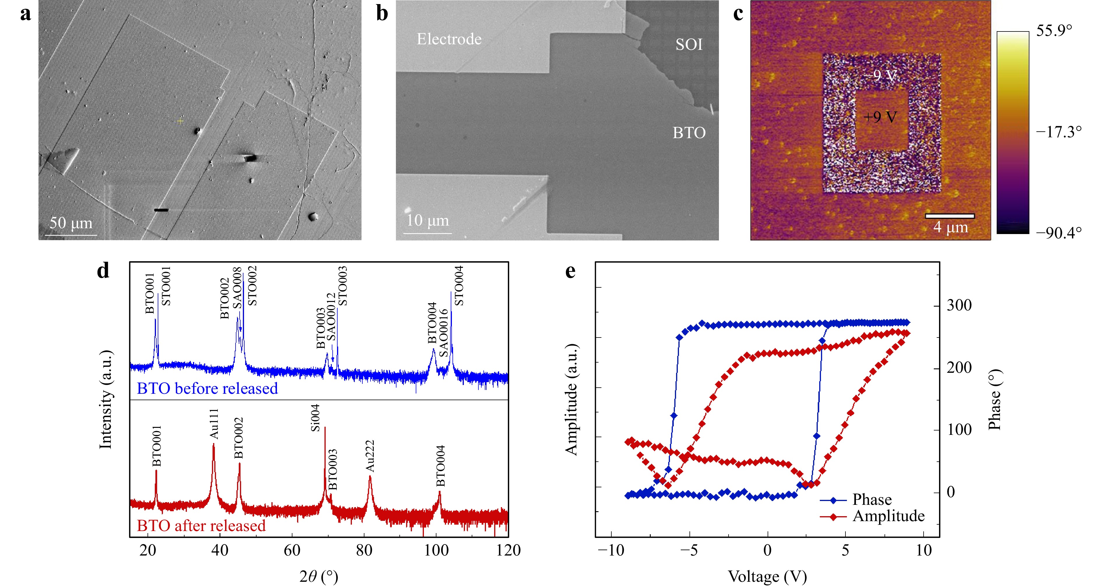
Fig. 3 a–b Plane-view Scanning Electron Microscope (SEM) images of Contact/BTO/SOI. c Piezoelectric force microscope (PFM) phase image of BTO writing domains under ±9 V. d XRD patterns of as-grown BTO/SAO/STO heterostructure and transferred BTO layer on the SOI. e PFM amplitude and phase hysteresis loops of BTO.
The red line in Fig. 3d illustrates the well-preserved (00l) diffraction peaks of BTO on the SOI substrate. In addition, the peaks of the BTO layer after transfer shifted slightly to a higher angle, proving that the epitaxial film lost the clamping effect from the substrate after release, and the stress in the BTO lattice was also released, thereby decreasing the lattice constant c. Through piezoelectric force microscopy, a conductive probe was used to apply a bias voltage from 9 V to -9 V on the BTO film, which was transferred onto the gold-coated Si substrate. Fig. 3e shows the local amplitude and phase hysteresis loops of the BTO film. A typical phase hysteresis loop was observed, proving that the BTO sample had good piezoelectric properties. However, the amplitude loop was not a symmetrical butterfly shape, and this condition is often attributed to defects or internal bias fields48. The internal bias field in single crystal films is often caused by oxygen vacancies and excess metal ions49. We believe that the asymmetrical amplitude response may be caused by defects and oxygen defects in the BTO films.
-
A more detailed analysis indicate that, BTO, a ferroelectric material, exhibits the structure of a crystal with tetragonal structure at a temperature of approximately 20 °C, containing a short a-axis and a longer c-axis50. Thus, the ferroelectric BTO is often to facilitate growth in various orientations via controlling the process parameters. There exists a relationship between the Pockels effect, and direction of the electrostatic field, direction of light propagation and polarisation, rotation angle of the crystal, and the thickness of the BTO thin films51. Previous studies have established that BTO exhibits an ordinary refractive index (no = 2.444) that is higher than the extraordinary index (ne = 2.383) because of the structure of a negative uniaxial anisotropic crystal52. Relatively, the growth of BTO crystals in different directions has different Pockels coefficients. The performance of the EO in each direction of the BTO crystal structure usually employs an elliptical equation as a simulation model. In the presence of electric fields (Ex, Ey, Ez), the BTO refractive index is expressed as
$$ \begin{split}&\left(\frac{1}{{{\mathrm{n}}_{0}}^{2}}+{\mathrm{r}}_{13}{\mathrm{E}}_{\mathrm{z}}\right){\mathrm{x}}^{2}+\left(\frac{1}{{{\mathrm{n}}_{0}}^{2}}+{\mathrm{r}}_{13}{\mathrm{E}}_{\mathrm{z}}\right){\mathrm{y}}^{2}+\left(\frac{1}{{{\mathrm{n}}_{\mathrm{e}}}^{2}}+{\mathrm{r}}_{33}{\mathrm{E}}_{\mathrm{z}}\right){\mathrm{z}}^{2}+\\&\left({\mathrm{r}}_{51}{\mathrm{E}}_{\mathrm{y}}\right)2\mathrm{y}\mathrm{z}+\left({\mathrm{r}}_{51}{\mathrm{E}}_{\mathrm{x}}\right)2\mathrm{z}\mathrm{x}=1 \end{split}$$ (1) where rij is the linear (or Pockels) EO coefficient. Here, according to the anisotropy of ferroelectric BTO, the EO coefficient varies in different directions (r13 = 8 pm/V, r33 = 28 pm/V,r51 = 800 pm/V)53. Integrating the BTO thin films on SOI waveguides for modulation, and increasing the effective Pockels coefficient of the BTO crystal $ {r}_{eff} $ plays a vital role in enhancing the effect of EO modulation. The $ {r}_{eff} $ of the BTO is expressed as
$$ \rm r_{eff}=\frac{\lambda g} {n^3 _{BTO}\Gamma_{BTO}V_{\text π}L}$$ (2) where $ \mathrm{\lambda } $ is the central wavelength of the light wave, g represents the separation space between contacts, $ {n}_{BTO} $ is the refractive index of the BTO, $ {\Gamma }_{BTO} $ is the EO overlap integral supposing a homogeneous electric field exists over the entire BTO, and $ {V}_{\text π } $ is the half-wave voltage of the modulator as measured. In particular, the Pockels effect in ferroelectric domains can be translated into a hysteresis response of the refractive index to the field, which is consistent with the polarisation of ferroelectric domains. When an electric field was applied to ferroelectrics, the electric domains expanded along the direction of the electric field, resulting in a greater degree of polarisation. By contrast, the electric domain in the direction parallel to the electric field decreased. As the electric field strength continued to increase, the crystal domains tended to be oriented in the electric field direction; thus, the polarisation strength tended to saturate. In this condition, the polarisation of the ferroelectric film is linearly related to the applied electric field if the applied voltage is increased4. The modulator refractive index change $ \mathrm{\Delta }\mathrm{n} $ is expressed as
$$ \mathrm{\Delta }\mathrm{n}=\frac{1}{2}{{\mathrm{n}}_{\mathrm{e}\mathrm{f}\mathrm{f}}}^{3}{\mathrm{r}}_{\mathrm{e}\mathrm{f}\mathrm{f}}\frac{\mathrm{V}\mathrm{m}\left(\mathrm{\omega }\right)}{\mathrm{g}} $$ (3) where $ {n}_{eff} $ is the effective refractive index of the waveguide (calculated using an FDE solver), V is the magnitude of the applied voltage and the polarisation of the film can be changed by adjusting the electric field, and $ {\rm m}\left({ \omega }\right) $ is the EO amplitude response at the microwave modulation angular frequency $ \mathrm{\omega } $.
It was assumed that the coordinate systems of the x-, y-, and z-axes of the indexing ellipsoid were aligned along the crystallographic axes a1, a2, and c of the BTO crystal structure, respectively. Consequently, the effective EO properties of BTO can be improved by rotating the ferroelectric film by a rotation angle φ in the xy plane, as shown in Fig. 4a. As mentioned previously, the effective Pockels coefficient of BTO strongly depends on its crystal orientation, rotation angle, and thickness. Hence, we sequentially optimised factors such as the orientation, rotation angle of BTO, and thickness of the thin films to achieve a high $ {\mathrm{r}}_{eff}. $ The equation indicates that the change in the effective refractive index of BTO has a strong dependence on $ {\mathrm{r}}_{\mathrm{e}\mathrm{f}\mathrm{f}} $; thus, $ \mathrm{\Delta }\mathrm{n} $ can be used to characterise the performance of the BTO-based modulators.
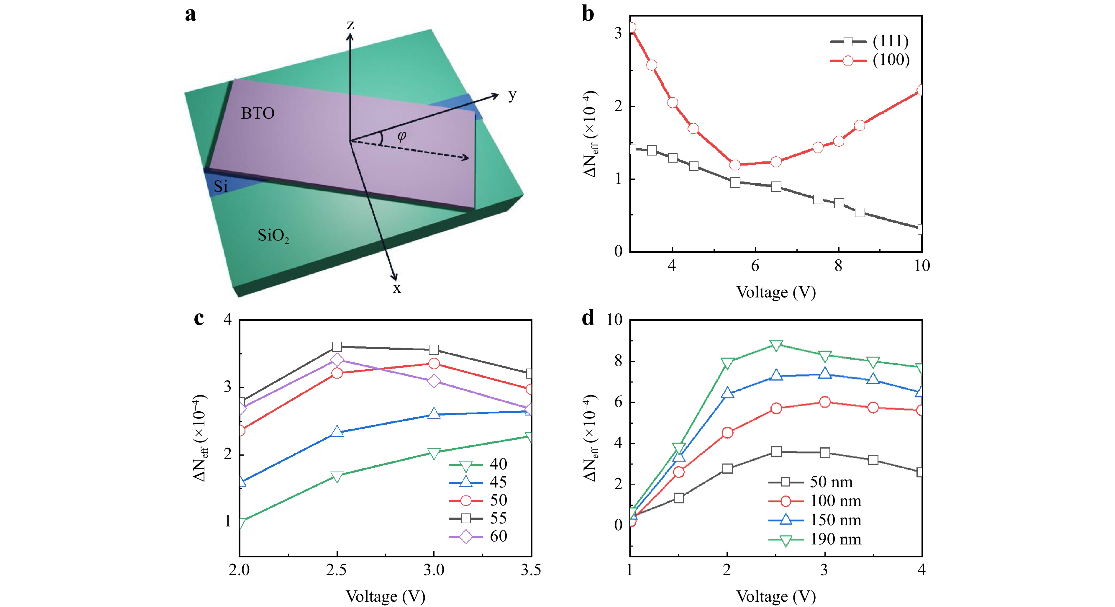
Fig. 4 EO properties of the modulators. a Change in the rotation angle φ of the transferred BTO films in the xy plane to improve the EO performance. b Curves of the effective refractive index difference $ \Delta {N}_{eff} $ as a function of applied voltages for (111)- and (100)-oriented BTO. c Curves of the effective refractive index difference $ \Delta {N}_{eff} $ as a function of applied voltages for BTO films with different rotation angle φ in the xy-plane. d Curves of refractive index difference $ \Delta {N}_{eff} $ as a function of applied voltages for different thicknesses of the BTO layer.
We first investigated the dependence of $ \mathrm{\Delta }\mathrm{n} $ on the lattice destinations of BTO thin films. Based on a previous study of BTO crystals54, it is known that the (110)-oriented BTO grows at a higher pressure than the other two orientations. However, higher oxygen pressures produce a large number of voids, whereas lower pressures favour the formation of uniform and smooth films. Therefore, considering the quality of the films, we compared (100)-oriented BTO with (111)-oriented BTO. The results are presented in Fig. 4b. From the phase hysteresis loops of BTO studied previously42, it is known that when the applied voltage exceeds a certain value, the phase change of BTO is slightly reduced. This was exhibited within the crystal as the polarisation strength of the ferroelectric domains became saturated.
The maximum value of $ \Delta \mathrm{n} $ was 3 × 10⁻⁴, which was achieved at (100)-oriented BTO. This value was used to calculate $ {\mathrm{V}}_{\text{π}}L $ of the modulator as 0.26 V$ \cdot \mathrm{c}\mathrm{m} $. Using Eq. 2, we can introduce the corresponding effective Pockels coefficient of 279 pm/V. As depicted in Fig. 4c, considering the dependence of $ \mathrm{\Delta }\mathrm{n} $ on the angle φ, we must optimise φ to obtain the best combination of r13, r33, and r51. The refractive index of the TE polarisation shifted from $ {n}_{0} $to $ {n}_{e} $when the angle was scanned across 0–90°. The maximum value (approximately 3.6 × 10⁻⁴) was reached for a rotation angle of 55°, and similar theoretical predictions were reached by Castera et al.51 and experimentally verified by Abel et al.26.
Note that the optimised angle is irrelevant to the waveguide because it is analysed based on the crystal nature of BTO. Finally, we studied the EO refractive index modulation as a function of the BTO thickness (Fig.4d). Increasing the thickness of the BTO layer tBTO caused a larger change in the $ {\mathrm{n}}_{\mathrm{e}\mathrm{f}\mathrm{f}} $. Nevertheless, it is more challenging to synthesise high-quality thick BTO layers. Consequently, we obtained the ideal thickness (approximately 150 nm) when the thickness of BTO was simulated across 50–190 nm to achieve the maximum phase shift, low half-wave voltage values, and high modulation efficiency.
-
We transferred a BTO film onto the MZI structure (Fig. S6). A schematic of the experimental setup is shown in the Supporting Information (Fig. S7). First, we investigated the transmission curves of the modulator before and after transferring the BTO layer to determine the loss caused by transferring the material to the modulator. The results showed that the output loss increased by approximately 1 dB after the transfer (Fig. S8). We then measured the transmission curves of the devices under different bias voltages to investigate the modulation efficiency of the BTO. Our device demonstrated an extinction ratio greater than 30 dB. The insertion loss of the entire device was approximately 18 dB, and the transmission loss of the device was 1 dB/cm.
Fig. 5a shows the device structure, wherein the propagation direction of light was parallel to the (100)-oriented BTO layer. The magnified microscope images in Fig. 5b show that the metal contacts (in yellow) were deposited on both sides of the Si waveguide (in white). The EO response of the device was tested in the communication band (approximately 1545 nm). Fig. 5c shows the transmission spectra at three different voltages. The electric field affected the refractive index of the films, which in turn modulated the phase of light55,56. Therefore, the phase equation can be expressed as:
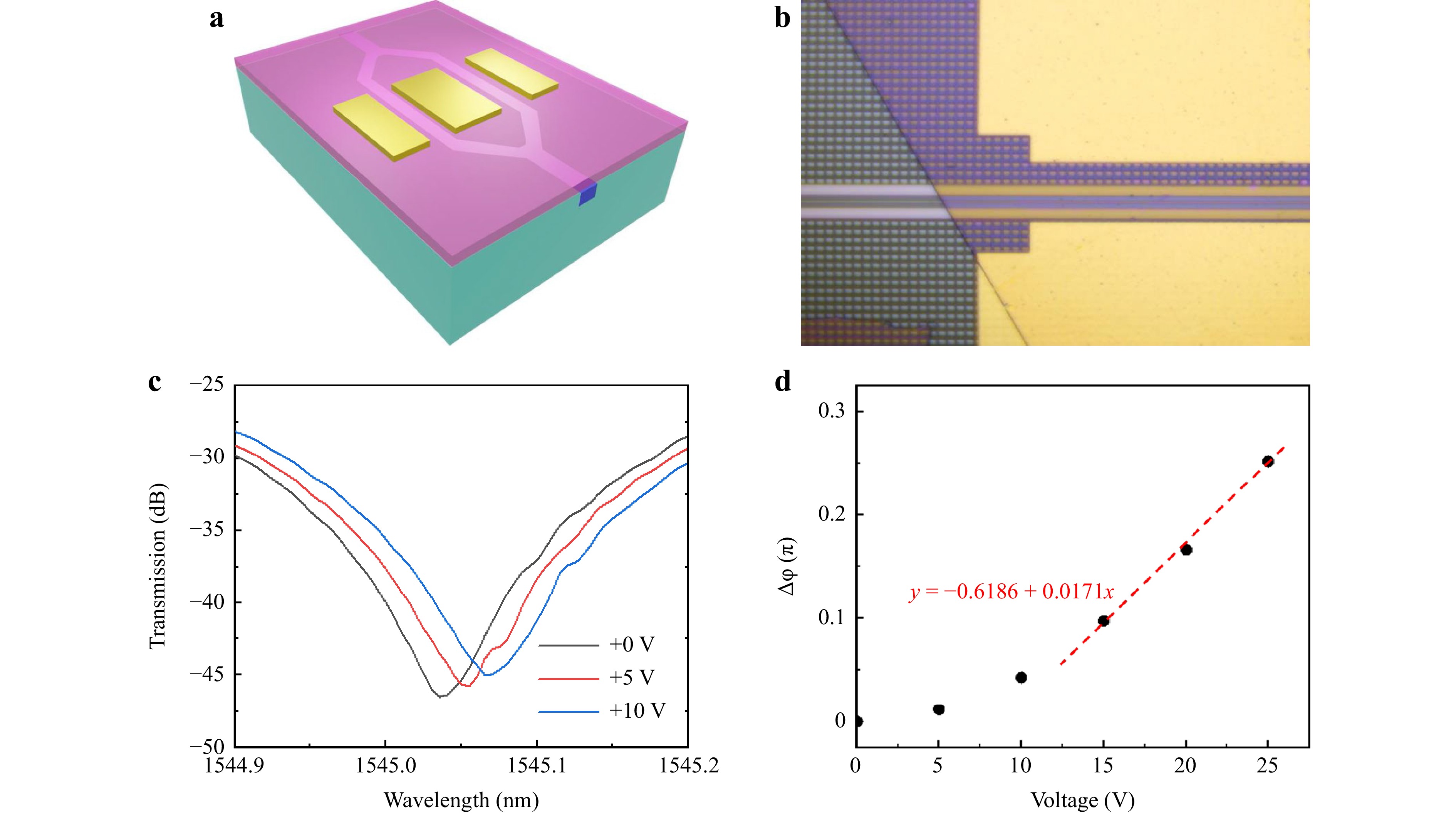
Fig. 5 BTO ferroelectric hybrid integrated modulators on SOI Platform. a Simulated schematic of the MZI device. The straight section of the MZI arm is parallel to the (100)-oriented of the BTO lattice. The length of the active region shown is 286 μm. b Optical micrograph of the MZI device at the waveguide. The yellow part of the picture is the contact and the part between the two white lines is the Si waveguide in which the optical signal is transmitted. c Measured transmitted light intensity spectra at selected voltages of +0 V, +5 V and +10 V. d The $ \Delta \mathrm{\phi } $ curve is calculated with respect to different voltages, with the red line being the tangential of the curve.
$$ \Delta {\phi }=\frac{2{\text{π }}\mathrm{L}}{\mathrm{\lambda }}\cdot \Delta \mathrm{n} $$ (4) Substituting (3) into (4) provides a general relationship between $ \Delta {\phi } $ and EO effects, as follows:
$$ \mathrm{\Delta }{\phi }=\frac{\text{π }\mathrm{L}}{{\mathrm{\lambda }}_{0}}{\mathrm{\Gamma }\mathrm{n}}^{3}{\mathrm{r}}_{\mathrm{e}\mathrm{f}\mathrm{f}}\frac{\mathrm{V}\mathrm{m}\left(\mathrm{\omega }\right)}{\mathrm{g}} $$ (5) Further, the half-wave voltage $ {V}_{\pi } $ is expressed as”
$$ {\mathrm{V}}_{\text{π }}=\frac{{\mathrm{\lambda }}_{0}\mathrm{g}}{{\mathrm{n}}^{3}{\mathrm{r}}_{\mathrm{e}\mathrm{f}\mathrm{f}}\mathrm{\Gamma }\mathrm{m}\left(\mathrm{\omega }\right)\mathrm{L}} $$ (6) Fig. 5d illustrates the phase change at different applied bias voltages (0–25 V) for the TE polarisation of light. The length of the active region L was 286 μm and Vπ was the voltage that triggered a π phase shift in the waveguide. The overall BTO MZI device footprint was 876 μm × 738 μm. The dependence of the induced phase shifts $ \mathrm{\Delta }{\phi } $ on the voltages are displayed in Fig. 5d. According to Eq. 4, we obtained the curve of $ \Delta \mathrm{n} $ with respect to the applied bias voltages (see Fig. S9).
When the electric field was small, certain ferroelectric domains remained in the opposite direction of the electric field. When the electric field was increased, the electric domains opposite to the direction of the electric field decreased. The electric domains expanded along the direction of the electric field, at which point there was a low degree of polarisation in the electric domains. Because the signals applied in our experiments were DC voltages, the polarisation of barium titanate triggered a ferroelectric hysteresis effect when small voltages were applied, which resulted in the modulator being in a nonlinear mode47. As the voltage increased, the curve became linear. As such we obtained the modulation efficiency VπL value as 1.67 V·cm.
According to Eq. 6, we can derive the effective Pockels coefficient reff as 48 pm/V in the experiment. The EO effect is related to the orientation of BTO, the uniformity of the lattice on the orientation, and the type and number of defects. The discrepancy between the simulation and experimental results can be explained by film defects and the hysteresis properties of the ferroelectric crystals. Different growth conditions affect the uniformity and defect density of the BTO films; thus, the growth conditions have an impact on device performance. Subsequently, the process could be further optimised using sacrificial layer materials with smaller lattice mismatches, such as Sr4Al2O757. The measured results were compared with other technologies and are summarised in Table 1. Compared to LiNbO317 BaTiO3, has a higher modulation efficiency. In contrast to the plasma dispersion effect of other techniques within Si, the Pockels effect is inherently lossless and ultrafast. Indium phosphide (InP) modulators58 offer high performance in established technologies; however, they struggle to compete with low-cost Si photonics owing to their specialised fabrication process. Eltes et al.30 and Z. Dong et al. used MBE and RF-sputter to deposit BTO. However, these studies used both bonding and buffer layers. By comparing these two methods, we demonstrated a method to transfer the BTO film onto the SOI for EO modulation with low losses using a much simpler process. Our BTO film does not need to be epitaxially grown or patterned, which greatly reduces difficulties in the fabrication process. To measure other parameters, a longer active region is necessary to further increase the modulation depth.
Table 1. Performance comparison of MZM based on different materials
-
In summary, a target-transfer method was used to transfer a BTO film onto a Si MZI for EO modulation. This transfer method simplified the fabrication process and produced high-quality BTO films on the SOI platform. As a proof of principle, we demonstrated a transferred BTO film on an MZI waveguide structure. Our MZI devices with $ {\text{V}}_{\text{π}} $L as low as 1.67 V·cm confirmed the excellent EO properties of the BTO films and their full compatibility with SOI substrates, thereby facilitating the realisation of compact EO modulators. The hybrid integration of BTO with SOI waveguides has broadened the Si photonics device library and paved the way for high-speed and high-efficiency EO modulators.
-
We used the transfer method to obtain (100)-oriented BTO thin films on target SOI substrates. On the Si substrate, the Si waveguide was buried in the oxide layer with a thickness of approximately 2 μm. The width and thickness of the Si waveguide were 500 nm and 220 nm, respectively. CMP was used to flatten the surface of the Si waveguide, leaving a thin layer of SiO2 of ~5 nm on top. The specific steps of the transfer method are as follows39.
-
In this experiment, SAO and BTO targets were synthesised using the solid-state sintering method. To obtain the SAO precursor, SrCO3 (99.95% purity) and Al2O3 (99.99% purity) were mixed in stoichiometric ratios. After ball milling, the mixture of SrCO3 and Al2O3 was dried, sieved, and calcined at 1250 °C for 2 h to obtain the SAO precursor powder. After the secondary ball milling process, the SAO target was sintered at 1450 °C for 4 h. BaTiO3 (99.99%) powder was directly sintered at 1250 °C for 2 h to obtain the BTO targets. The BTO/SAO bilayer was deposited on commercial (001)-oriented STO substrates via a pulsed laser deposition method using a KrF excimer laser at a wavelength of 248 nm. In the process, we set the temperature for growth, laser energy density, and dynamic oxygen pressure for SAO as 800 °C, 2.0 J/cm3, and 0.2 mbar, respectively. In contrast to SAO, we set the temperature for growth, laser energy density, and dynamic oxygen pressure for BTO to 750 °C, 1.8 J/cm3, and 0.15 mbar, respectively.
-
During the transfer, a thin layer of photoresist was spin-coated onto the surface of BTO/SAO/STO (100) as a support layer, and heated the sample at 115 °C for 25 min to dry the photoresist layer. The samples were then immersed in deionised water for 24 h to remove the SAO layer. Subsequently, the photoresist/BTO films were transferred onto the target SOI substrates to ensure the target rotation angle between the BTO film and the MZI waveguide structure. The photoresist layer was completely removed with anhydrous acetone, and the BTO films were successfully transferred onto the SOI substrates. Finally, to provide a modulating electric field, metal contacts were formed by 5 nm titanium and 80 nm Au, using electron beam lithography (EBL), which were placed on the BTO layer and aligned symmetrically on both sides of the Si waveguide.
-
We acknowledge the funding from the National Key Research and Development Program of China (2019YFB2205303), National Natural Science Foundation of China (62205054, 62375051, and 52002310), Natural Science Foundation of Jiangsu Province (BK20210207), and Fundamental Research Funds for Central Universities.
Towards high quality transferred barium titanate ferroelectric hybrid integrated modulator on silicon
- Mengxue Tao1,
- Butong Zhang2,
- Tianxiang Zhao1,
- Xiaoxuan Wu1,
- Ming Liu2,
-
Guohua Dong2, *, ,
 ,
, -
Junjia Wang1, *, ,
- Light: Advanced Manufacturing 5, Article number: 31 (2024)
- Received: 24 October 2023
- Revised: 16 May 2024
- Accepted: 21 May 2024 Published online: 14 October 2024
doi: https://doi.org/10.37188/lam.2024.031
Abstract: Silicon photonics is currently the leading technology for the development of compact and low-cost photonic integrated circuits. However, despite its enormous potential, certain limitations, such as the absence of a linear electro-optical (EO) effect because of the symmetric crystal structure of silicon remain. In contrast, barium titanate (BTO) exhibits a strong Pockels effect. In this study, we demonstrated a high-quality transferred barium titanate ferroelectric hybrid integrated modulator on a silicon-on-insulator platform. The proposed hybrid integration of BTO on silicon Mach-Zehnder interferometers exhibited EO modulation with a VπL as low as 1.67 V·cm, thereby facilitating the realisation of compact EO modulators. The hybrid integration of BTO with SOI waveguides is expected to pave the way for the development of high-speed and high efficiency EO modulators.
Research Summary
Target-transfer method: a new way to realize barium titanate hybrid integrated modulator on silicon
Silicon photonics is currently the leading technology for the development of compact, low-cost photonic integrated circuits. The strong Pockels effect exhibited by barium titanate (BTO) makes it a popular material for hybrid integrated modulators on silicon. Researchers from Southeast university and Xi'an Jiaotong University demonstrated a high-quality transferred barium titanate ferroelectric hybrid integrated modulator on a silicon-on-insulator (SOI) platform. The target-transfer method simplifies the fabrication process and promotes high quality BTO films on SOI. As a proof-of-concept, the team demonstrated electro-optical (EO) modulation with VπL as low as 1.67 V∙cm confirmed the excellent EO characteristics of transferred BTO films and their full compatibility with SOI substrates, facilitating the realisation of compact EO modulators.
Rights and permissions
Open Access This article is licensed under a Creative Commons Attribution 4.0 International License, which permits use, sharing, adaptation, distribution and reproduction in any medium or format, as long as you give appropriate credit to the original author(s) and the source, provide a link to the Creative Commons license, and indicate if changes were made. The images or other third party material in this article are included in the article′s Creative Commons license, unless indicated otherwise in a credit line to the material. If material is not included in the article′s Creative Commons license and your intended use is not permitted by statutory regulation or exceeds the permitted use, you will need to obtain permission directly from the copyright holder. To view a copy of this license, visit http://creativecommons.org/licenses/by/4.0/.

 DownLoad: