


-
Proteins are natural organic materials that have been utilized for thousands of years1. Natural protein materials have recently gained attention owing to their potential applications in medicine2, sensing3, anti-counterfeiting4, textile electronics5, radiative cooling6, and information storage7. Silk fibroin is a typical natural protein derived from the silk produced by silkworms or spiders, and can be transformed into different forms including fibers, hydrogels, sponges, and transparent films using processes such as spinning, spin-coating, and chemical treatments8. Silk films have gained considerable attention owing to their facile chemical functionalization, unique optical properties, remarkable mechanical characteristics, and good biocompatibility9,10. By processing the surface structures, the properties of silk films can be modulated, and specific functionalities can be imparted. Silk protein in films can have different crystal forms including random coil, β-sheet, and helix11. Owing to their unique structure, silk films have been applied in cutting-edge fields such as brain-machine interfaces12, implantable bioelectronics13, biomedical diagnosis14, organic photovoltaics15,16, triboelectric nanogenerators17,18, information encoding19, and photoresists20,21. The processing of multifunctional structures on silk films is essential for their practical applications.
Conventional processing methods for fabricating micro/nanostructures on silk films primarily depend on electron beam lithography, ion beam lithography, near-field infrared nanolithography, ultraviolet lithography, nanoimprint lithography, inkjet printing, and template-assisted patterning22–27. Electron-beam and ion-beam lithography23 have accuracies of <20 nm and require a high-vacuum environment. Near-field nanolithography provides a spatial resolution of approximately 35 nm7 and relies on complex systems to maintain a precise spacing between the probe and silk film. Nanoimprint lithography24, ultraviolet lithography25, and template assisted patterning28 can be used to process nanostructures on large-area. However, the ease of processing is limited by the prerequisite manufacturing of templates or masks. Inkjet printing26 is a large area patterning method, which has an accuracy of approximately 5 μm. Additionally, the crystal forms of silk fibroin can affect the morphology of the processed structures27,29–31. For instance, the structural transition of a silk film from a crystalline form to a short polypeptide was utilized to process craters, whereas the structural transition from an amorphous to helical form was employed to process pillars20. Nevertheless, these processing techniques have limitations such as time-consumption, imprecision, uncontrollability, and the reliance on vacuum working conditions. Therefore, the controllable fabrication of complex micro/nanostructures on silk film surfaces in air remains challenging.
Ultrafast laser is a micro/nano processing tool with the advantages of a high precision, no mask requirement, controllability, and reproducibility32,33. Ultrafast lasers have been used to process micro/nanostructures, submicron patterns, and functional devices34–36, including supercapacitors37,38, photodetectors39,40, refractive index sensors41, optical encryption devices42, photoelectrodes43, memristors44, soft machinery45, and flexible sensors46. Owing to the ultrashort periods and ultrahigh energy intensities of ultrafast laser pulses, the interaction between ultrafast lasers and materials is a complex process involving energy deposition, transfer, structural transformation, plasma emission, and ablation at different temporal and spatial scales47,48. Multiphoton absorption and ionization are critical mechanisms of laser-dielectric interactions owing to the absence of conduction-band electrons in dielectric materials49. Plasma ablation or structural transformations can occur in ionized materials, resulting in the removal or modification of the material50. Furthermore, various micro/nanostructures can be fabricated by controlling the absorption and energy deposition of ultrafast lasers. For example, ultrafast lasers have been used to process two-dimensional materials into three-dimensional objects51,52, pattern hydrogel templates53, and print three-dimensional quantum dot architectures54. To the best of our knowledge, ultrafast lasers have only been used to process single silk fibres55,56, and induce the polymerization of silk-fibroin solution57. However, the controllable fabrication of specific structures on silk films remains elusive, and the interactions between ultrafast lasers and protein films should be investigated for practical functional device applications.
In this study, we propose an ultrafast laser-processing method for creating crater/bulge structures by bulging and ablating a protein film. By controlling the interaction between the ultrafast laser and silk film, bulges and craters of different morphologies and sizes were processed, which may be used for inkless color printing. The formation mechanisms of these structures were studied using light-field calculations and material characterization. The developed method was used to process functional optical devices including holograms and Fresnel zone plates. This study expands our understanding of the ultrafast laser processing of protein films and broadens the ability to modify and improve their properties for practical device applications.
-
Fig. 1a presents a bulge processed using an ultrafast laser pulse. The bulge had a width of 600 nm, length of 1050 nm, and height of 214 nm. Owing to the dielectric properties of the silk film, multiphoton absorption dominates the interaction between the silk films and strong laser field56. The absorption spectra of the silk film are presented in Fig. 1b on a logarithmic scale along the y-axis. The absorbances of the silk film were 1.5% at 800 nm and 92.4% at 267 nm, corresponding to three-photon absorption. Fig. 1c presents the absorption of the silk films as a function of the peak power of the ultrafast laser. When the peak power was less than 500 GW/cm2, the silk film was nearly transparent to the ultrafast laser. In contrast, nonlinear absorption occurred when the laser peak power exceeded 500 GW/cm2. These results suggest that three-photon absorption is the dominant mechanism in the processing of silk films using ultrafast lasers. Silk films have gained significant attention as optical materials owing to their transparency and ease of preparation on different substrates58. Ultrafast lasers provide a facile micro/nano processing method for the development of protein-based optical devices. The concept of ultrafast laser processing of an optical encryption device is illustrated in Figure S1 and Movie S1. Other optical devices with various functions can be fabricated by patterning different structural arrays using ultrafast lasers.
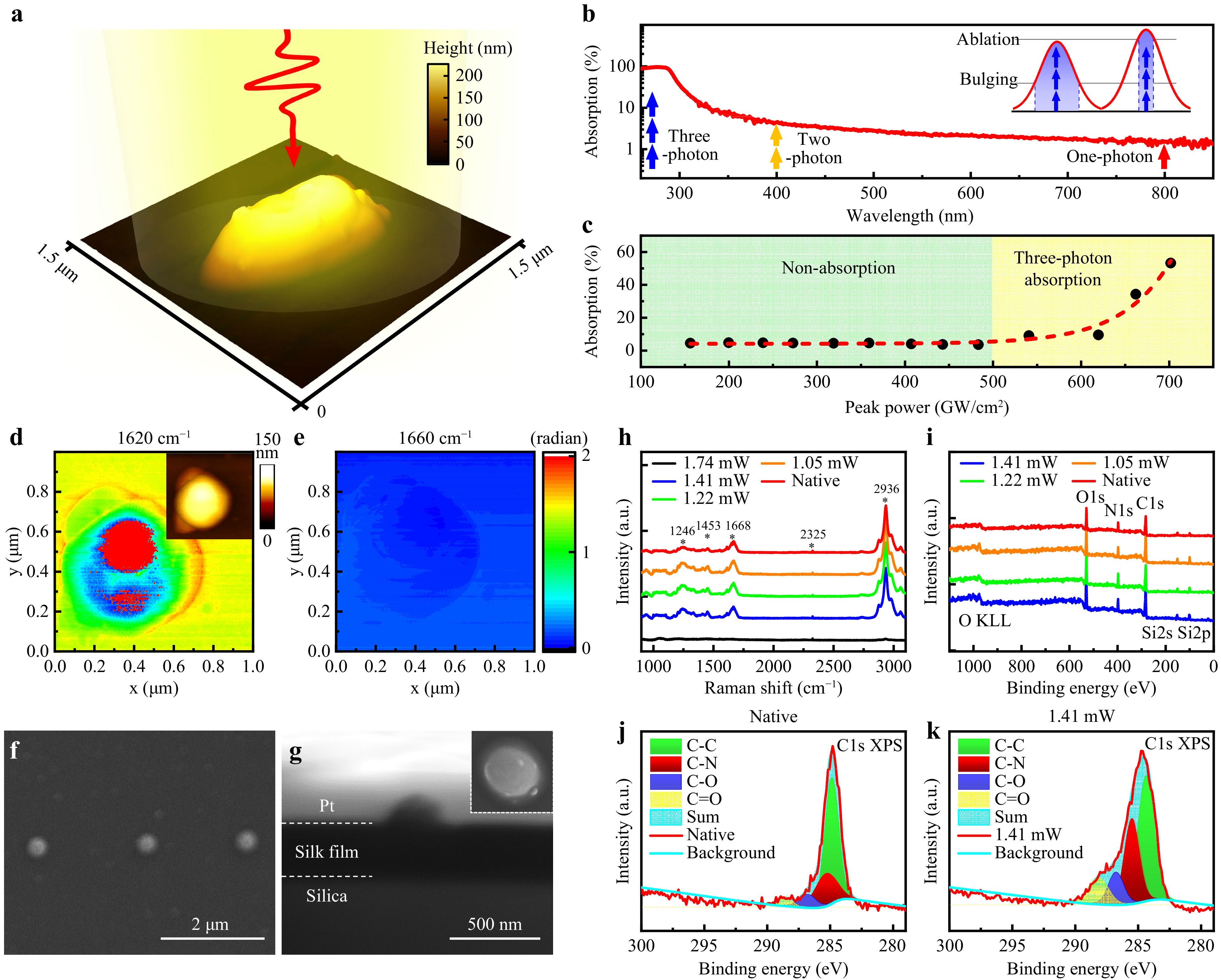
Fig. 1 Formation of bulges in a silk film using an ultrafast laser. a AFM image of a bulge processed with an ultrafast laser pulse. b Absorption spectrum of a silk film, with a logarithmic scale on the y-axis. c Absorbance of the silk film as a function of the peak power of an ultrafast laser. d, e Nano-IR phase images of a laser-processed bulge. f Surface and g cross-sectional SEM images of a bulge processed with an ultrafast laser. h Raman spectra and i XPS profiles of the silk film before and after ultrafast laser processing. High-resolution XPS C1s profiles of a j native silk film and k silk film processed with an ultrafast laser of 1.41 mW power.
The mechanisms underlying the formation of bulges during the processing of a silk film using an ultrafast laser were studied. Figure S2a presents a schematic of the silk film preparation and bulge processing. First, fibroin was regenerated by sericin removal, dissolution, dialysis, and centrifugation8 (see Methods for more details). Subsequently, a silk film was fabricated via spin-coating and solidification. The silk fibroin in the silk film was in the form of random coils and demonstrated to be water-soluble20. Therefore, the silk film cannot be washed with water. Silk films undergo crystal-form transitions in response to external stimuli, such as UV radiation, energetic electrons, or specific chemicals19–21. In this study, an 800-nm, 35-fs linearly polarized laser was used (Figure S3). The femtosecond laser pulse irradiated onto the silk film had a pulse width that was slightly larger than 35 fs owing to the chirp introduced by the optical components. The pulse width was measured to be approximately 80 fs using an optical pulse autocorrelator. The formation of bulges on the silk film can be attributed to the transition of the crystal form of the silk protein, as illustrated in Figure S2b and S2c. To explore the formation mechanism of the bulges, their chemical compositions were investigated using nano-infrared imaging, Raman spectroscopy, and X-ray photoelectron spectroscopy (XPS).
Fig. 1d, e present the nano-IR phase images of a laser-processed bulge with wavenumbers of 1620 and 1660 cm−1. The inset of Fig. 1d displays an atomic force microscopy (AFM) image of the bulge. The phase contrast between the nano bulge and unprocessed silk film in the near-field resembles the absorbance spectra in the far-field, exhibiting a higher contrast at the peaks of the infrared absorption59; it exhibits a higher contrast at 1,620 cm−1 (Fig. 1d), indicating the formation of crystalline β-sheet structures20. The helical structures should display a resonance absorbance peak at 1660 cm−120; it exhibits a lower contrast at 1660 cm−1 (Fig. 1e). This result indicates that β-sheet is the dominant protein structure of the bulged silk film. The same conclusion was obtained by analyzing the nano-IR phase images of the bulges generated by laser pulses with pulse energies ranging from 323 to 328 nJ (Figure S4). To study the interior morphology of the bulge, a focused ion beam (FIB) was used to section a single bulge; the corresponding scanning electron microscopy (SEM) images are presented in Fig. 1f, g. Figure S5 demonstrates the enlarged cross-sectional SEM image of the bulge. The interior of the bulge had a continuous structure similar to that of the silk film that was not irradiated by the ultrafast laser, and no evidence of voids or cracks was observed.
Fig. 1h presents the Raman spectra of the silk films before and after laser irradiation. The native silk film yielded five Raman peaks at 1246, 1453, 1668, 2325, and 2936 cm−1. The Raman bands at 1246 cm−1 (attributed to amide III, N-H in-plane bending, and CH2 twisting)60,61, 1453 cm−1 (attributed to CH3 anti-symmetric bending in polyalanine and CH2 bending in polyalanylglycine)60, 1668 cm−1 (attributed to amide I and C=O stretching in β-sheets)60,62,63, and 2936 cm−1 (attributed to CH2 stretching)64 exhibit negligible shifts upon processing with an ultrafast laser of less than 1.74 mW power. When processed at a power of 1.74 mW, the silk film was ablated (Figure S6d), revealing only the Raman band at 2325 cm−1. The Raman bands at 2325 cm−1 may be attributed to the N-N stretching of the interstitial N2 in the silica substrate65. The preservation of the four Raman peaks after irradiation with the ultrafast laser indicates that the molecular structure of the silk film remained unchanged during laser processing. As shown in Figure S6, the optical microscopy images reveal a color change of the silk film processed with ultrafast lasers at power levels ranging from 1.05 to 1.41 mW. The region processed by the laser exhibits bright areas. In contrast, the utilization of a long pulse laser such as a nanosecond laser (1064 nm) or CO2 laser (10.6 μm) may result in the destruction of the chemical structure of the silk film (Figure S7).
Fig. 1i presents the XPS profiles of the native and laser-processed silk films, which exhibited peaks corresponding to O1s, N1s, and C1s. After being processed with ultrafast lasers of different powers ranging from 1.05 to 1.41 mW, the XPS profiles of the silk film remained similar to that of the native silk film. Fig. 1j and 1k present the high-resolution C1s XPS profiles of the native and laser-processed silk films, respectively, where the XPS peaks corresponding to C-C, C-N, C-O, and C=O were observed for the native silk film. These XPS peaks were maintained after processing with an ultrafast laser with a power of less than 1.51 mW (see Figure S8a-S8c for more information). The same results were obtained by analyzing the O1s and N1s profiles (Figure S8d and S8e). The atomic concentrations of carbon, oxygen, and nitrogen were consistent before and after laser processing, as shown in Figure S8f and Table S1. The preservation of the XPS peaks and consistency of the atomic concentrations indicate that the molecular structure of the silk film remained unchanged during ultrafast laser processing.
-
Four types of structures were generated on the silk film using an ultrafast laser, as shown in Fig. 2. As the laser pulse energy or number of pulses increased, the morphologies of the structures evolved, resulting in the formation of cracks, bulges, nanocraters, and microcraters (Fig. 2i). When both the pulse energy and number of pulses were low, no modification of the refractive index or diffraction effect was observed on the silk film (Figure S9); the zone marked in red in Fig. 2i corresponds to this case. However, when the number of pulses was high and the pulse energy was low, cracks formed owing to the near-field-enhanced effect; this corresponds to the purple zone in Fig. 2i. The near-field enhancement effect has been discussed in our previous study55. Bulges formed when the silk film was processed with a single pulse with an energy of approximately 326 nJ, as indicated by the yellow zone in Fig. 2i. In other scenarios, the silk film ablated and craters formed. Nanocraters formed when the silk film was irradiated with a single pulse with an energy greater than 336 nJ. Fig. 2e–h present the SEM images of a crack (e), bulge (f), nanocrater (g), and microcrater (h) generated by using an ultrafast laser. Fig. 2a–d present the laser-intensity distributions calculated under the corresponding conditions, which determine the distribution of energy deposition. The results of the calculations and SEM images indicate that the micromorphologies of the laser-processed structures correspond to the distribution of laser energy.
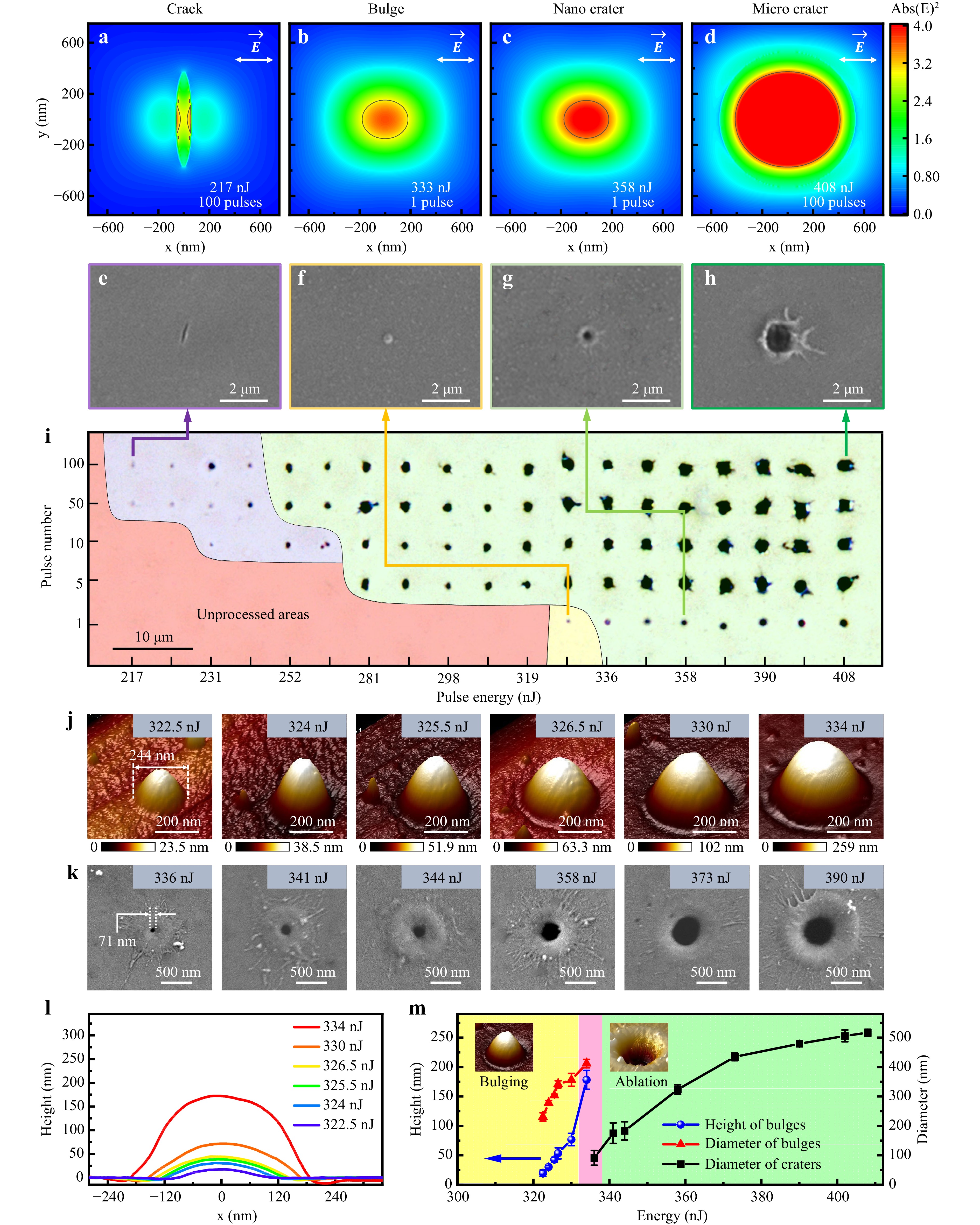
Fig. 2 Morphological evolution of laser-processed structures on a silk film. Results of the light-field distribution calculated for a 100 pulses with an energy of 217 nJ, b one pulse with an energy of 333 nJ, c one pulse with an energy of 358 nJ, and d 100 pulses with an energy of 408 nJ. SEM images of a laser-processed e crack, f bulge, g nanocrater, and h microcrater. i Morphological evolution of the structures as the pulse energy and number of pulses increases. j AFM images of the bulges processed with laser pulses of different energies ranging from 322.5 to 334 nJ. k SEM images of craters generated using laser pulses with pulse energies ranging from 336 to 390 nJ. l Cross-sectional profiles of the bulges shown in j. m Relationship between the size of the laser-processed structure and pulse energy.
Subsequently, we examined the micromorphologies of the bulges and craters processed with single laser pulses of varying energies ranging from 322.5 to 390 nJ. Fig. 2j presents the AFM images of the bulges processed using laser pulses with pulse energies ranging from 322.5 to 334 nJ. Fig. 2l presents cross-sectional profiles of the bulges shown in Fig. 2j, which have smooth and round surfaces, suggesting that no ablation or plasma eruptions occurred. Craters formed when the pulse energy exceeded 336 nJ, as shown in Fig. 2k. The surface morphologies of the craters are shown in Figure S10. Fig. 2m presents the relationship between the size of the laser-generated structure and energy of the laser pulse; the crater size increased as the pulse energy increased. A bulge with a diameter of 244 nm and a height of 18 nm was generated when an ultrafast laser pulse with an energy of 322.5 nJ was used, whereas a crater with a diameter of 71 nm was generated using a 366 nJ laser pulse. The experiment was repeated several times, demonstrating that the nano-and microstructures were reproducible when the silk films were prepared in different batches using the same method. As shown in Figure S11, the modulus of the silk film decreased after laser processing. The Derjaguin–Müller–Toporov (DMT) modulus of the bulges and laser-ablated holes remained at approximately 5 GPa. The Ti:sapphire laser regenerative amplifier system used in this study can generate 1000 pulses per second. A single bulge or crater can be processed in 1 ms, and patterned arrays of bulges or craters can be processed by moving the laser-focusing spot within the pattern, as illustrated in Figure S12. Compared with techniques such as electron/ion beam lithography, near-field nanolithography, and template-assisted patterning, this approach does not require a high-vacuum environment, templates, masks, or probes, as shown in Table S2. However, certain potential challenges remain for practical applications, such as the need to further improve the processing efficiency.
The shapes of the craters and bulges were determined from the light field distribution of the laser beam. Spatial light-shaping techniques can be used to reshape the light-field distribution of an original Gaussian beam into a patterned light field66. Craters or bulges with patterned shapes can be processed on silk films using reshaped pulses. A slit was used to reshape the Gaussian beam into an elliptical light field. Figure S13a presents the optical setup for slit-based spatial light shaping. Figure S13b–d present the simulated intensity profiles in the planes at the focal point, after passing through and in front of the slit. Figure S13e and S13f show the cross-sectional profiles and AFM images of the strip-shaped structures processed using the reshaped ultrafast laser pulses. The strip-shaped bulges shown in Fig. 1a were processed using a slit-based spatial shaping method.
The electron density during the ultrafast laser irradiation was also studied. As demonstrated in Fig. 1b, three-photon absorption is the dominant mechanism for initiating the ionization process. The dynamics of electron density were calculated using the plasma model proposed in our previous study55. The optical properties of the silk films subjected to femtosecond laser irradiation were estimated using the Drude model43. The dynamics of the laser intensity, calculated electron density, and spatial distribution of the electron density are shown in Figure S14. According to calculations, plasma ablation occurs when the electron density is higher than 1.34 × 1023 cm−3. The crater diameters were estimated by comparing the spatial distribution of the electron density with the threshold value (Figure S14d). The calculated crater diameters shown in Figure S14e sufficiently agreed with the measured values. We assumed that bulging occurs when the electron density is higher than 1.22 × 1023 cm−3 and calculated the diameters of the bulges (Figure S14f). The variational trend of the measured bulging diameters was similar to that of the calculated bulging diameters. These results suggest that the localized ionization achieved by the three-photon absorption may be responsible for the generation of craters and bulges.
-
These results demonstrate the precision and efficiency of the ultrafast laser processing for patterning arrays of craters and bulges on silk films. Microstructural arrays were patterned on silk films for inkless color printing, and different colors were achieved by adjusting the center-to-center spacing between the microstructures. Fig. 3a presents the dark-field optical micrographs of the microstructural arrays with center-to-center distances ranging from Λ = 1 μm to Λ = 2.5 μm. Fig. 3b presents the CIE1931 chromaticity coordinates of the colors presented in Fig. 3a, which ranged from orange to blue, indicating the coloration ability of the method. The simulated scattering spectra of the microstructures (Fig. 3h) reveals that a blue shift occurs as the center-to-center distance decreases. In particular, as the center-to-center distance was decreased from Λ = 2.5 to 1 μm, the color gradually shifted from purple to blue owing to the grating diffraction effect42. The variational trend in the simulation results was consistent with the experimental results. Figure S15 presents the dark-field optical micrographs of the microstructures with varying diameters while maintaining a constant center-to-center distance of 1.2 μm. The brightness increases as the diameters of the microstructures increase; however, the color remains blue. The color changes were owing to the center-to-center distances. The created structures and colors remained stable after exposure to an open environment for 33 months (Figure S16). Fig. 3c presents a laser-processed pattern that reads “Tsinghua” captured with a dark-field optical microscope. The pattern appeared colorful under white-light illumination. The letters were composed of microstructural arrays with different center-to-center distances ranging from Λ = 0.75 to 1.75 μm. Fig. 3d presents an SEM image of the pattern. The varying grayscale of the SEM image was owing to the differences between the structural arrays in each letter. Fig. 3e presents partially magnified SEM images of the five microstructural arrays in Fig. 3d, and Fig. 3f presents the AFM image of the bulge array in letter “a”. The distance between the bulges was Λ = 0.75 μm. This method was used to print images with dimensions of hundreds of micrometers67. For example, Fig. 3g (right) presents the laser-processed pattern of an auditorium building; the reference image is shown on the left.
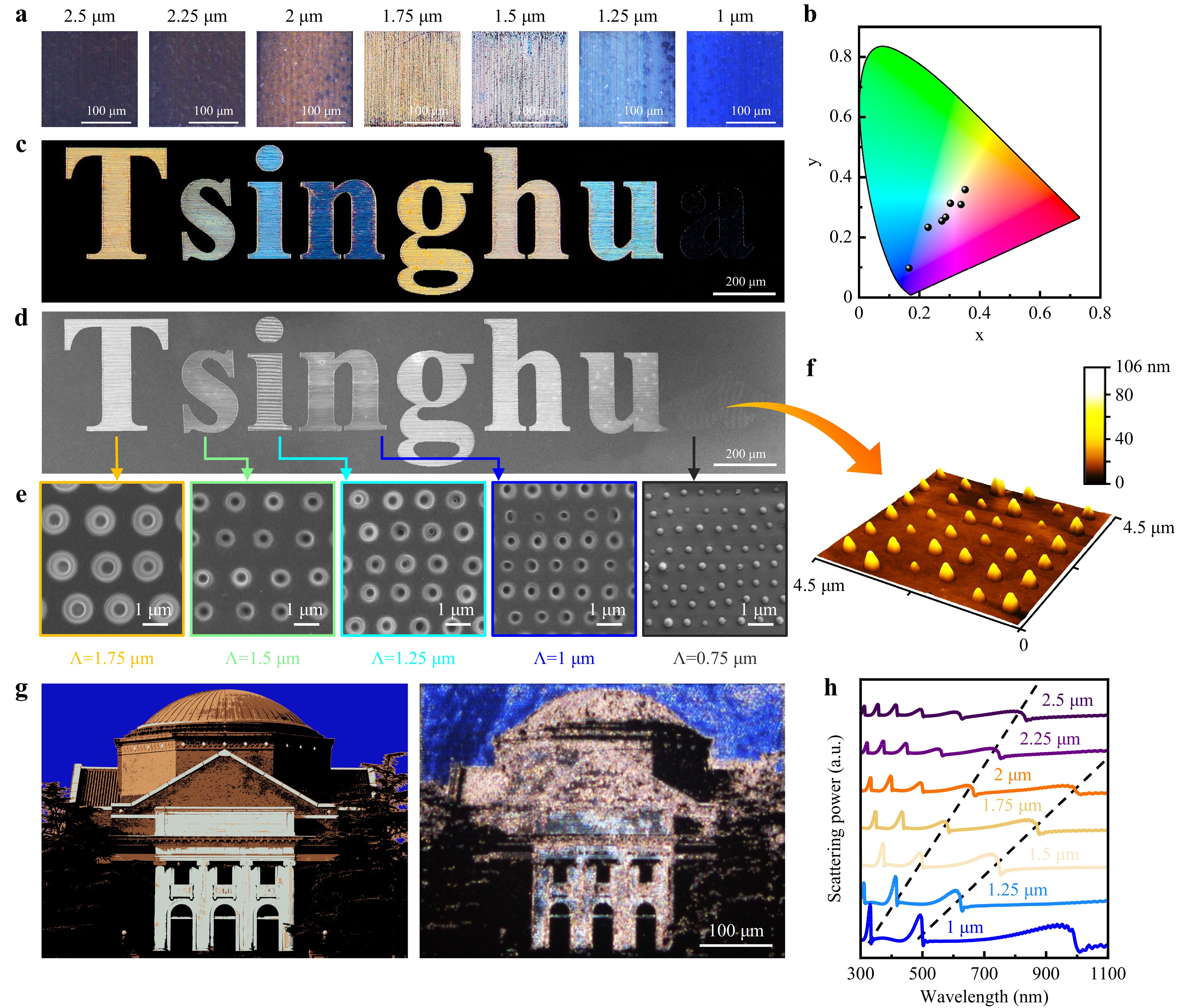
Fig. 3 Processing of microstructural arrays on a silk film for inkless color printing. a Color palette of microstructural arrays. b CIE1931 chromaticity coordinates of the colors shown in a. c Dark-field optical micrograph of a pattern that reads “Tsinghua,” and d SEM image of the pattern. e Partially magnified SEM images of microstructural arrays. f AFM image of the bulge array in letter “a.” g Reference image and the laser-processed pattern of an auditorium building. h Simulated scattering spectra of microstructural arrays with center-to-center distances ranging from 2.5 to 1 µm.
-
Organic optical functional devices such as holograms and Fresnel zone plates were processed using an ultrafast laser. Fig. 4a presents the experimental setup used to acquire the holographic images. After passing through a beam expansion system and an iris, a 530-nm illumination laser was irradiated onto the hologram, and the holographic images were reconstructed on a white screen. The hologram of the dog was computed using the Gerchberg–Saxton algorithm. The hologram contained 200 × 200 pixels, with each pixel having a width of 5 μm. Fig. 4b, c present the original image and the calculated hologram of the dog, whereas Fig. 4d presents the simulated results of the hologram. Fig. 4e presents an optical micrograph of the hologram processed using the ultrafast laser, and Fig. 4g shows a magnified view of this optical micrograph, where the black and white regions represent the laser-ablated and non-ablated areas, respectively. Owing to the difference between the refractive indices of the silk film and air, the illumination laser was deflected in different directions upon passing through the hologram and the holographic image was reconstructed (Fig. 4f).
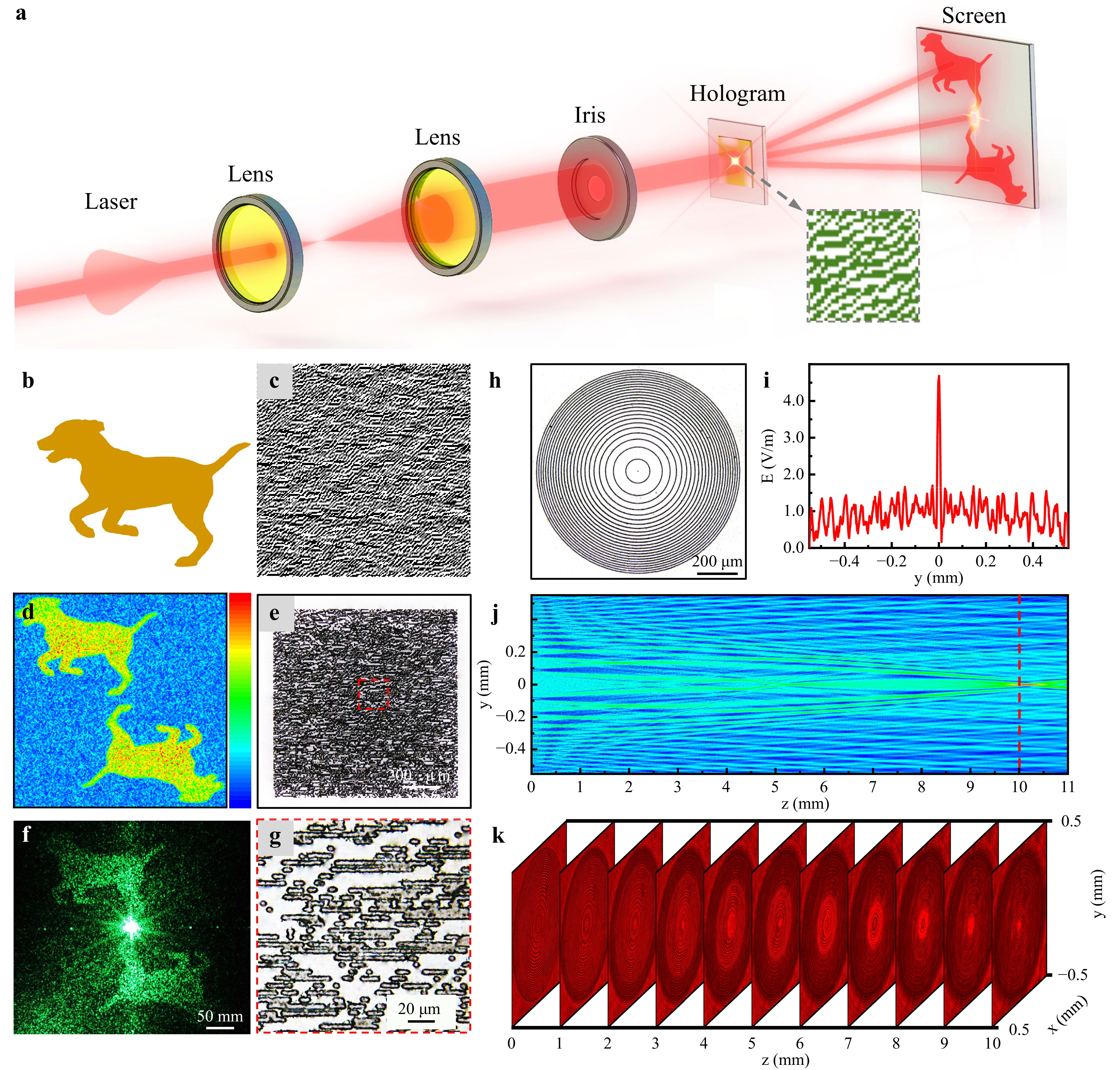
Fig. 4 Holographic and Fresnel optical devices processed with an ultrafast laser. a Experimental setup used for the optical testing of a hologram. b Original image and c calculated hologram of a dog. d Simulated intensity distribution of the calculated hologram. e Optical micrograph of the hologram and g a magnified view. f Reconstructed holographic image captured with a camera. h Optical micrograph of an ultrafast laser-processed Fresnel zone plate. j Simulated and k experimental distribution of the light-field intensity behind the Fresnel zone plate.
A Fresnel zone plate with a focal length of 10 mm was designed and processed using an ultrafast laser. Fig. 4h presents an optical micrograph of the Fresnel zone plate, which can be used as an objective lens in the optical path. Fig. 4i, j present the simulated distributions of the light-field intensity for an illumination beam passing through a Fresnel zone plate; the illumination beam was focused at z = 10 mm. The experimental setup for the optical testing of the Fresnel zone plate is illustrated in Figure S17a. After passing through the iris, the Fresnel zone plate was irradiated using a laser. The distribution of the light-field intensity was then evaluated using a charge-coupled device (CCD) camera. Fig. 4k presents the experimentally obtained distribution of the light-field intensity (see Figure S17b for more details). The illuminated beam was focused at z = 10 mm, which was consistent with the simulation results.
-
This study demonstrates an ultrafast laser processing method for silk films that modulates bulging and ablation. We demonstrated that the transition of the crystal form of the silk protein and plasma ablation are responsible for the bulging and ablation of the silk film, which cannot be achieved using commonly used metals or dielectrics. A bulge with a diameter of 244 nm and crater with a diameter of 71 nm were generated. This method provides a facile approach for the fabrication of various organic optical functional devices. The strip-shaped craters and bulges were processed using a slit-based spatial shaping method. Inkless color printing was achieved by processing organized microstructural arrays with varying center-to-center distances. In addition, a computed hologram was processed, and a holographic image was reconstructed. We also presented a Fresnel zone plate that can focus the illumination laser. This study introduces a path for the fabrication of organic optical functional devices and can be readily extended to process other protein materials, resulting in new opportunities in cutting-edge fields for these natural materials.
-
Preparation of silk films: First, silkworm cocoons were cut into small pieces and placed in boiling water with 5 wt% NaHCO3 for half an hour to remove sericin. The degummed silk fibers were then air-dried. Degummed silk fibers (2.0 g) were added to 10 ml of LiBr solution (9.3 mol/L) to form a silk fiber/LiBr solution. The container with the silk fiber/LiBr solution was sealed and heated at 60 ℃ for 4–6 h to obtain a fibroin (protein) solution, which was dialyzed against ultrapure water for 48 h and centrifuged to obtain a 7% aqueous silk fibroin solution, which was stored at 4 ℃ until use, and spin-coated (SETCAS, KW-4A, China) onto a silica substrate at 3000 rpm for 30 s to obtain a silk film with a thickness of 500–1000 nm and then air dried.
Ultrafast laser processing: To process the silk film, an 800-nm, 1-kHz, 35-fs linearly polarized laser was employed (Coherent, Astrella, USA), the polarization of which was controlled using a half-wave plate. The pulse energy was regulated using a neutral-density filter. The laser beam was focused using a 50× microscope objective (Olympus, LMPLFLN 50×, Japan, NA = 0.5). The silk film was fixed to the positioning stage (200-nm minimum incremental motion) for laser processing.
Simulation: The distribution of the laser intensity was calculated using a three-dimensional finite-difference time domain (FDTD) method. The simulated system was consistent with the experimental setup. An 800-nm laser with a Gaussian distribution was linearly polarized and focused on the surface of the silk film. The finite-element method (Comsol EWBE) was used to simulate the illumination light-field behind the optical device.
Morphological and structural characterization: The microstructures of the silk samples were characterized using scanning electron microscopy (SEM, ZEISS, Gemini300, Germany). The acceleration voltage was 3 kV, and a secondary electron detector (SE2) was used. The morphology of the silk samples was characterized using atomic force microscopy (AFM, Bruker, Dimension, Germany) in the tapping mode. Nano-IR images were captured using a scattering-type SNOM (Neaspec GmbH, Germany) at wavenumbers of 1620 and 1660 cm−1. Raman spectra were recorded using a Raman spectrometer (Horiba LabRAM HR Evolution, France, 532 nm, 1-µm spot size). XPS measurements were performed using an XPS instrument (UlvacPhi, PHI Quantera II, Japan).
-
This research was supported by the National Natural Science Foundation of China (52075289), China Postdoctoral Science Foundation (2023M731942), the Shuimu Tsinghua Scholar Program of Tsinghua University, and the Tsinghua-Jiangyin Innovation Special Fund (TJISF, 2023JYTH0104). We would like to thank Dr. Fei Gu and Dr. Xi Lu at Quantum Design for their assistance with the nano-IR image measurements.
Ultrafast laser processing of silk films by bulging and ablation for optical functional devices
- Light: Advanced Manufacturing , Article number: (2024)
- Received: 19 September 2023
- Revised: 10 April 2024
- Accepted: 11 April 2024 Published online: 12 July 2024
doi: https://doi.org/10.37188/lam.2024.024
Abstract: Organic proteins are attractive owing to their unique optical properties, remarkable mechanical characteristics, and biocompatibility. Manufacturing multifunctional structures on organic protein films is essential for practical applications; however, the controllable fabrication of specific structures remains challenging. Herein, we propose a strategy for creating specific structures on silk film surfaces by modulating the bulging and ablation of organic materials. Unique surface morphologies such as bulges and craters with continuously varying diameters were generated based on the controlled ultrafast laser-induced crystal-form transition and plasma ablation of the silk protein. Owing to the anisotropic optical properties of the bulge/crater structures with different periods, the fabricated organic films can be used for large-scale inkless color printing. By simultaneously engineering bulge/crater structures, we designed and demonstrated organic film-based optical functional devices that achieves holographic imaging and optical focusing. This study provides a promising strategy for the fabrication of multifunctional micro/nanostructures that can broaden the potential applications of organic materials.
Research Summary
Ultrafast laser: Fabrication of organic optical functional devices
Proteins, natural organic materials utilized for thousands of years, exhibit various excellent properties, including unique optical properties, remarkable mechanical characteristics, and biocompatibility. Researchers from the Department of Mechanical Engineering at Tsinghua University proposed a strategy for creating specific structures on silk film surfaces by modulating the bulging and ablation of organic materials. By controlling the interaction between the ultrafast laser and silk film, bulges and craters of different morphologies and sizes were processed, which may be used for inkless color printing. The developed method was used to process functional optical devices including holograms and Fresnel zone plates. This study introduces a path for the fabrication of organic optical functional devices and can be readily extended to process other protein materials.
Rights and permissions
Open Access This article is licensed under a Creative Commons Attribution 4.0 International License, which permits use, sharing, adaptation, distribution and reproduction in any medium or format, as long as you give appropriate credit to the original author(s) and the source, provide a link to the Creative Commons license, and indicate if changes were made. The images or other third party material in this article are included in the article′s Creative Commons license, unless indicated otherwise in a credit line to the material. If material is not included in the article′s Creative Commons license and your intended use is not permitted by statutory regulation or exceeds the permitted use, you will need to obtain permission directly from the copyright holder. To view a copy of this license, visit http://creativecommons.org/licenses/by/4.0/.

 DownLoad: