


-
Wearable devices have seamlessly become integrated into everyday life. Flexible pressure sensors are pivotal components of these devices. Their importance is heightened by the utilization of pressure as a primary mode of interaction in human settings. Thus, wearable technologies utilizing flexible pressure sensors have made significant strides in finding applications in human–machine interaction1,2, health monitoring3,4, and electronic skin5-7. These sensors are instrumental in driving societal advancements and enriching quality of life. Pressure sensors can be categorized as resistive, capacitive, piezoelectric, and frictional types8-12.
Compared with other types of pressure sensors, capacitive pressure sensors have been widely studied owing to their robustness, swift dynamic responses, low power consumption, etc.13,14. However, they suffer from an inherent limitation of low sensitivity. This is currently solved by embedding a micropattern into the electrodes or dielectric layers, which are tailored to augment the sensitivity and align with real-world application demands15-17. This strategy creates air gaps within the sensing layers, resulting in a low equivalent Young’s modulus Ee and equivalent dielectric constant εe. The foundational capacitance equation, C = εA/d, positions ε parallel to εe, with A denoting the effective electrode area, and d representing the inter-electrode distance. When the sensor is subjected to an external pressure, the low Ee value helps the sensor deform more easily; therefore, d is significantly reduced. As the sensor deforms, the air gap becomes occupied and εe increases significantly. Consequently, the capacitance C fluctuates significantly compared with that of flat, microstructure-free substrates.
Various micropatterns, such as micropillars18,19, microspheres20,21, micropyramids22, and microcones23, have been investigated and introduced into dielectric or electrode layers. Hua et al.24 compared nine different microstructures, including cylinders, spheres, pyramids, and cones, and explored their sensitivities under the same conditions. The conical structures exhibited the highest sensitivity to pressure changes. Common preparation methods for microcone structures include natural template lithography, laser engraving, and grayscale lithography. Wan et al.25 used lotus leaves as templates to reproduce a cone-like array microstructure consistent with the surface structure of lotus leaves. However, this technique lacks universality owing to the fixed microstructures of natural templates. Qu et al.26 used the laser engraving of wood to produce cone-like microstructures. This laser ablation method exhibits excellent micromorphology control; however, it has a low production efficiency and depends on expensive high-power and high-precision lasers. Grayscale lithography is characterized by the conversion of binary exposure in traditional lithography to grayscale exposure. Considering the limitations of using photomasks in conventional lithography, Gao et al.27 employed a maskless grayscale digital lithography method based on a digital micromirror device (DMD) to prepare various micropattern structures, including microcone structures. Li et al.28 fabricated microlens structures that were applied to pressure sensors based on the grayscale digital lithography method, and they yielded remarkable results. The preparation of microcone structures using grayscale lithography and their application in pressure sensors requires further investigation; however, the DMD-based optical system has a complex setup. Therefore, the production of highly sensitive capacitive pressure sensors through the simple and efficient preparation of cone-like microstructures with various morphologies remains challenging.
In a previous study29, we focused on alternating bright and dark laser speckle patterns and developed a maskless exposure method for the high-contrast photoresist SU-8 2025 using laser speckle lithography. After a series of processing steps, electrode layers with micropillar array structures were obtained and applied to capacitive pressure sensors, yielding a sensitivity of 2.14 kPa-1 within a pressure range of 0–100 Pa.
The autocorrelation function of the laser speckle intensity follows a first-order Bessel function of the first kind: The spatial distribution of the speckle intensity has a wavy shape and can be used as an exposure source field for grayscale lithography. This study developed a novel approach for fabricating microstructures based on laser speckle intensity patterns and grayscale characteristics. A low-contrast photoresist SPR220-7 (Dow Chemical) was exposed using an ultraviolet laser speckle field. Photoresist molds with various forms of random conical array (RCA) microstructures were obtained through dedicated grayscale lithography processes such as controlling the speckle size and exposure dose. Subsequently, these microstructures were transferred to polydimethylsiloxane (PDMS) via a two-step process, followed by the sputtering of a gold film on the PDMS surface to create PDMS electrodes. A thin polyvinylidene fluoride (PVDF) film was sandwiched between two PDMS electrodes, and an additional PDMS frame was used for encapsulation and protection. Finally, a flexible capacitive pressure sensor was fabricated with the highest sensitivity of 19.76 kPa−1 in the low-pressure range of 0–100 Pa. The sensor exhibited a rapid response time and detection limit of 131 ms and 1.9 Pa, respectively, and it remained stable without fatigue after more than 10,000 pressure cycles. The fabricated sensor was used to monitor respiratory rates and facial expressions. Furthermore, tactile testing was performed using a robotic arm to evaluate the sensor response to various soft and hard objects. These results highlight the excellent stability, durability, and accuracy of the sensor.
-
The following optical products were used to design the laser speckle exposure system: a 360 nm ultraviolet laser (Changchun New Industry Optoelectronic Tech, UV-F-360-PL), shutter (Thorlabs, SH1/M), beam expander (Thorlabs, BE05-10-A), mirror, convex lens (Thorlabs, LB1437-A), and engineering diffuser (Thorlabs, ED1-S20-MD). Fig. 1a depicts the light path used to generate the laser speckle. A UV laser served as the light source and a shutter was used to precisely control the exposure time. The beam expander enlarged the initial beam, whereas the mirror adjusted the light path. The convex lens focused the light, whereas the engineered diffuser ensured uniform illumination and generation of laser speckles (i.e., the laser speckle light field was uniform within the exposure area). The laser speckle traversed a free-space propagation light path, and a wafer coated with a photoresist was exposed to the speckle field. For a circular scattering spot, the autocorrelation function ΓI for the laser speckle intensity Ī follows a first-order Bessel function of the first kind, expressed as30
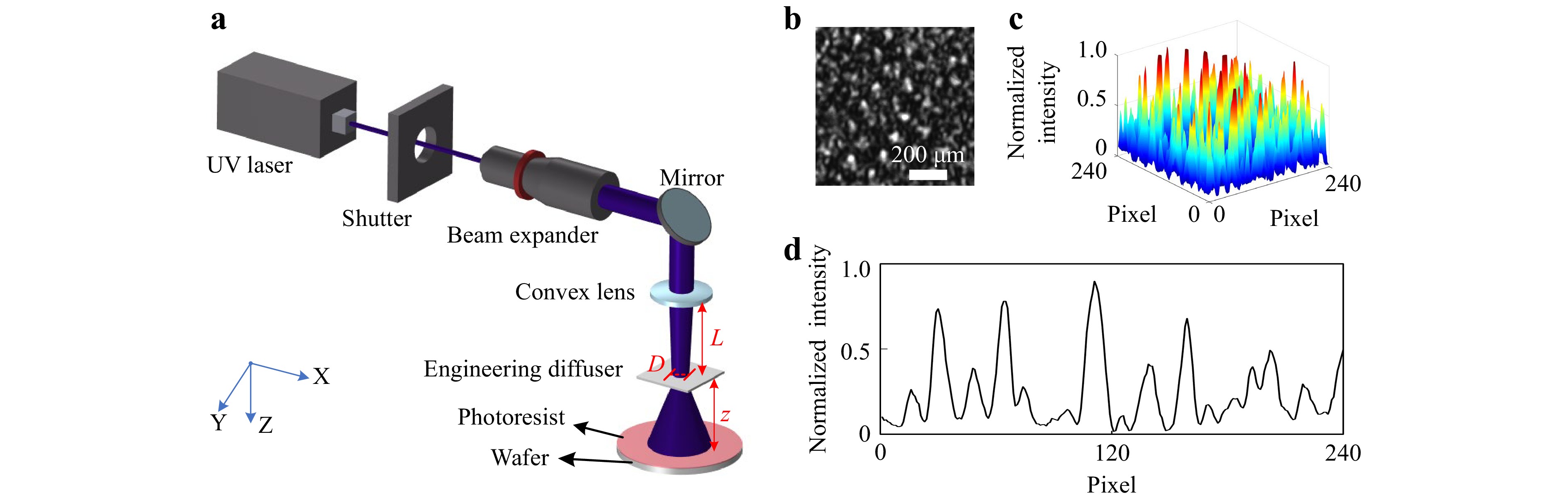
Fig. 1 Design of the laser speckle exposure system. a Schematic representation of the laser speckle exposure system, comprising the UV laser, shutter, beam expander, mirror, convex lens, engineering diffuser, and wafer coated with photoresist. b Image of the laser speckle captured using a machine vision camera. c Normalized three-dimensional intensity distribution derived from b. d Normalized two-dimensional intensity profile of the 13th row of b.
$$ {\Gamma _I}\left( r \right) = {\overline I ^2}\left[ {1 + {{\left| {2\dfrac{{{J_1}\left( {\frac{{\pi Dr}}{{\lambda z}}} \right)}}{{\left( {\dfrac{{\pi Dr}}{{\lambda z}}} \right)}}} \right|}^2}} \right] $$ (1) where λ is the UV laser wavelength, which was 360 nm in this study, z is the distance between the scattering (i.e., the engineering diffuser) and observation (i.e., the wafer) surfaces, D is the scattering spot diameter, and r denotes the distance between two arbitrary points on the observation surface. The first-order Bessel function of the first kind is similar to a decaying sine function, which ultimately causes the curve of the autocorrelation function to exhibit a wavy shape; therefore, such a light field of laser speckles can be used for grayscale exposure. In the one-dimensional case, the speckle size σ can be considered as the value of r based on the autocorrelation function, where J1(πDr/λz) first decreases to zero31. The first zero point of J1 is when πDr/λz = 1.22π, yielding the following one-dimensional speckle size σ:
$$ \sigma = 1.22\frac{{\lambda z}}{D} $$ (2) The value of σ depends on z and D. Here, z cannot be extremely large because the engineering diffuser has a divergence angle of 20°. The distance between the engineering diffuser and wafer is inversely proportional to the exposure power on the wafer. Hence, the entire system requires a long exposure time, which is detrimental to the stability of speckle lithography. Additionally, D cannot be excessively small because the engineering diffuser requires it to be greater than 0.5 mm. Therefore, we fixed z = 30 mm and adjusted L, which is the distance between the convex lens and engineering diffuser, using the Z-axis displacement platform to vary D. In this optical system, a parallel beam with a diameter of ~8.8 mm (after beam expansion) was incident on the surface of a convex lens with a focal length of 150 mm. Based on the principle of geometric optics, the setup was designed with the following parameters: L1 = 60 mm, L2 = 105 mm, L3 = 127.5 mm, and L4 = 135 mm, resulting in scattering spot diameters of D1 = 5.28 mm, D2 = 2.64 mm, D3 = 1.32 mm, and D4 = 0.88 mm, respectively. By applying the one-dimensional speckle size formula, we obtained σ1 = 2.5 μm, σ2 = 5 μm, σ3 = 10 μm, and σ4 = 15 μm. To gain an intuitive understanding of the spatial distribution of the laser speckle intensity using this laser speckle exposure system, we captured a representative laser speckle image using a machine vision camera (PixeLINK, PL-B781U). Because the pixel pitch in the camera was 3.5 μm, the speckle image was obtained with a one-dimensional speckle size of σ4 = 15 μm to ensure its maximum accuracy. Fig. 1b shows the laser speckle pattern with bright and dark distributions (the image resolution was 240 × 240 pixels). The grayscale matrix in Fig. 1b was calculated using MATLAB and then normalized to obtain the distribution of the speckle pattern intensity in three-dimensional space, as shown in Fig. 1c. One row (the 13th row) of the normalized grayscale matrix in Fig. 1b was selected to obtain the distribution of the speckle pattern intensity in two-dimensional space, as shown in Fig. 1d. Fig. 1c, d show that the surface profile of the laser speckle intensity exhibited an approximate RCA morphology, thereby providing a foundation for the preparation of RCA microstructures.
-
The photoresist SPR220-7, which is a low-contrast positive photoresist based on Novolac resin, was used in the experiments32. In the laser speckle grayscale lithography, SPR220-7 was exposed to a laser speckle optical field, thereby reproducing the laser speckle intensity distribution on the photoresist after it was developed. Fig. 2a–f show the fabrication of the microstructures on the photoresist using laser speckle grayscale lithography. First, the wafer was ultrasonically cleaned with acetone, isopropanol, and deionized water. Thereafter, it was dried on a hot plate at 150 °C to remove the surface moisture. The wafer surface was treated with oxygen plasma using a vacuum plasma treatment instrument (Guangzhou SunJune Tech, VP-R series) to activate it and improve its adhesion to the photoresist (Fig. 2a). The photoresist was deposited on the wafer surface using a spin coater. A pre-spin-coating step was performed at 500 rpm for 10 s, followed by the main spin-coating step at 2000 rpm for 30 s (Fig. 2b), resulting in a photoresist film thickness of approximately 9 µm. Subsequently, the wafer was transferred to a hot plate at 115 °C for 5 min to rapidly evaporate the solvent on the photoresist and enhance its adhesion to the wafer (Fig. 2c). After a short cooling period, the wafer was placed in an assembled optical system for exposure (Fig. 2d). After 60 min of exposure, the wafer was immersed in a Petri dish containing the developer for 3 min (Fig. 2e). Finally, deionized water was used for rinsing until no developer residue remained on the surface, and nitrogen gas was used for drying, resulting in a microstructured photoresist mold (Fig. 2f).
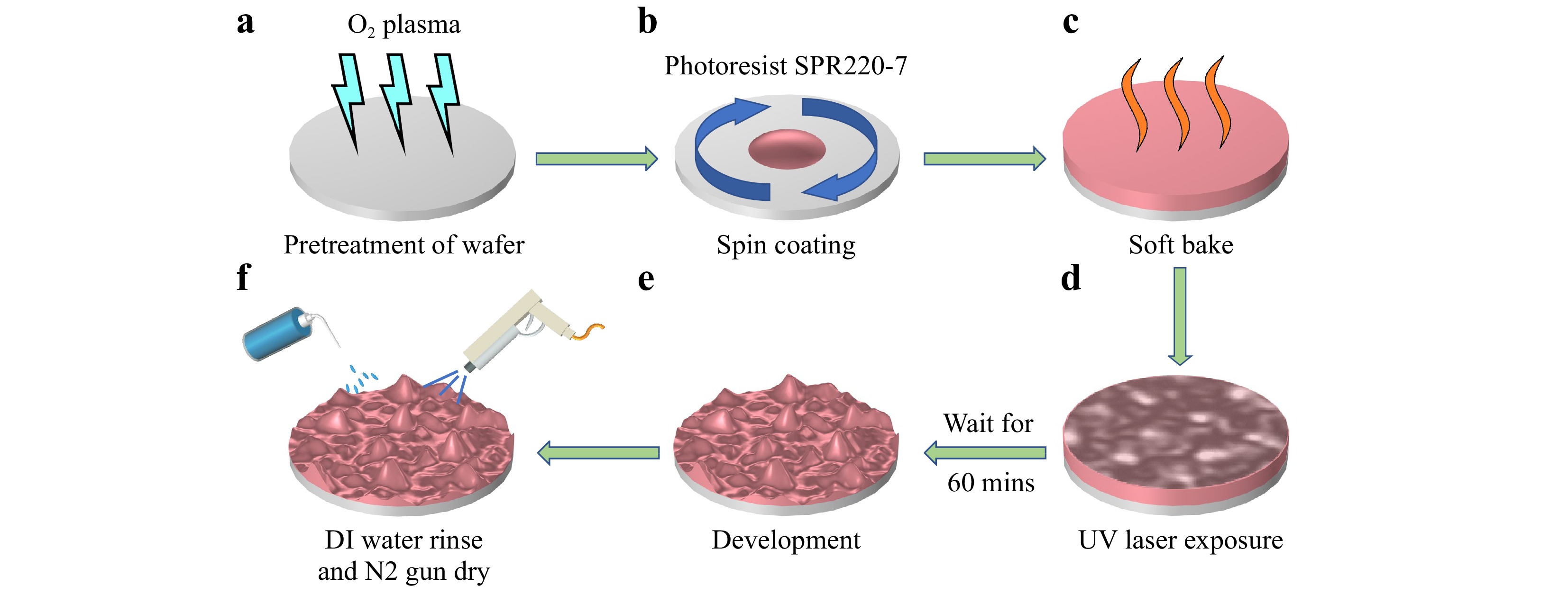
Fig. 2 Preparation of the microstructured photoresist SPR220-7 mold. a O2 plasma treatment of the wafer. b Spin coating of -7 on the wafer. c Soft baking of the photoresist on the wafer. d Exposure of photoresist using UV laser speckle. e Resulting microstructured photoresist mold after developing the substrate. f Photoresist mold rinsed with deionized water and dried using a N2 gun.
To obtain a photoresist with RCA microstructures, we must appropriately select the exposure dose, which represents the average energy density of the exposed laser speckle light field. The exposure dose can be regulated by controlling the exposure time. Because of the alternating distribution of bright and dark light in the laser speckle pattern, the light field can be considered a natural optical mask with an exposure similar to that in traditional lithography. The average power density of the exposed light field on the photoresist surface was measured as ~6 mW/cm2 using an integrating sphere photodiode power sensor (Thorlabs, S142C). As shown in Fig. 3a, a low exposure time of 17 s indicated underexposure (the exposure dose was ~100 mJ/cm2). The exposed areas on the photoresist were parts of the upper layer of the bright spot areas of the speckle field. An exposure time of 50 s indicated normal exposure (the exposure dose was ~300 mJ/cm2). The exposed depth of the photoresist located in the bright spot areas reached the wafer surface. However, the dark spot areas were nearly unexposed (SPR220-7 has a low response to exposure doses below ~20 mJ/cm2)33,34. An exposure time of 100 s indicated overexposure (the exposure dose was ~600 mJ/cm2); the exposure of the photoresist in the dark spot areas was initiated. As shown in Fig. 3b–d, the one-dimensional speckle size was fixed at σ2 = 5 μm, and three-dimensional profiles of the microstructured photoresist molds were obtained using atomic force microscopy (AFM) corresponding to the exposure conditions of Fig. 3a. As shown in Fig. 3e–g, a suitable line was selected from the three AFM images (Fig. 3b–d), and the corresponding two-dimensional contour curves of the microstructures were plotted. Based on the characterization diagram, the photoresist mold exhibited RCA microstructures during overexposure. Because of the uniform illumination of the engineering diffuser, the RCA microstructures exhibited consistent morphologies (see Fig. S1 in Supplementary Information).
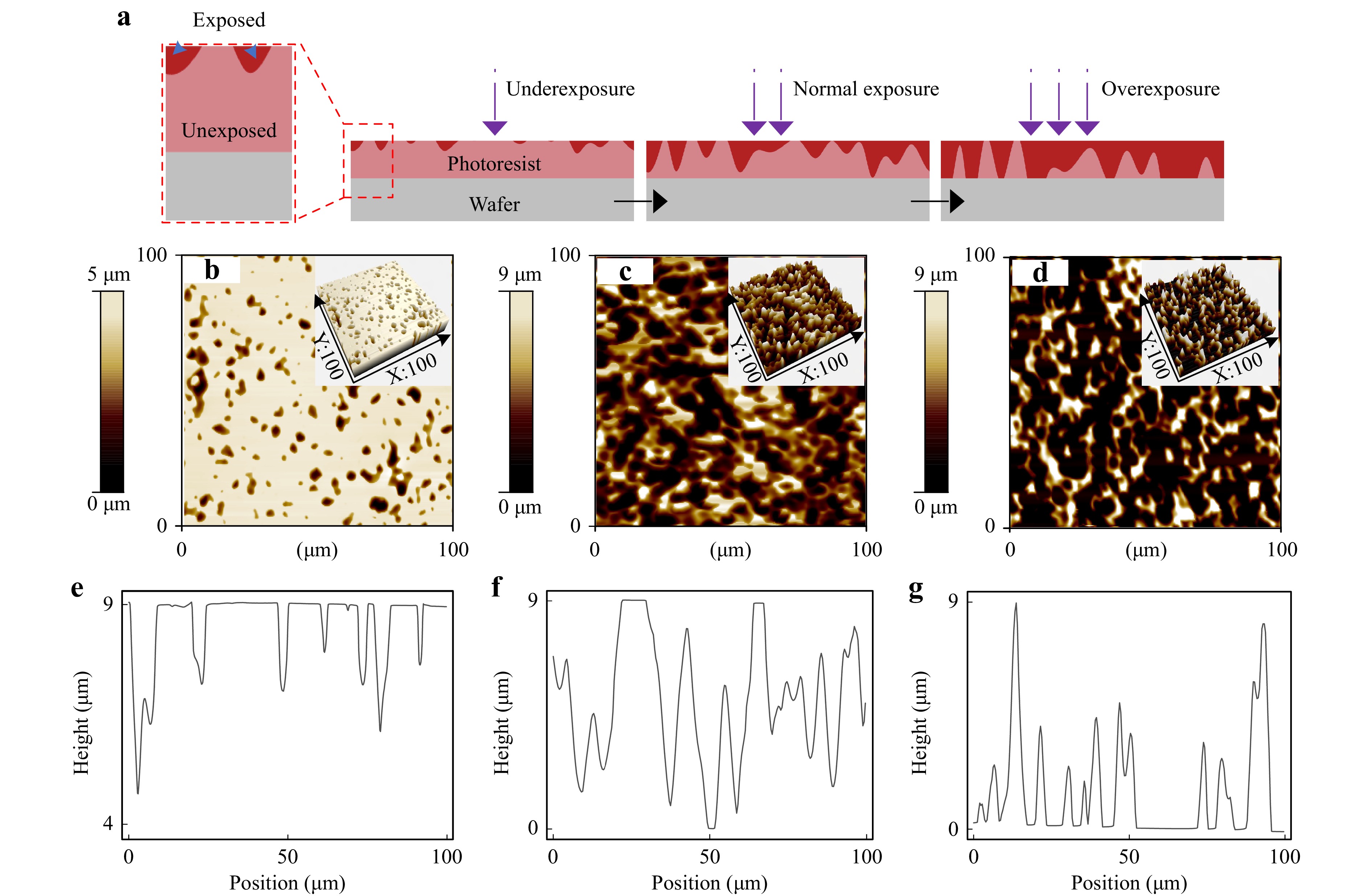
Fig. 3 Effect of different exposure conditions on the microstructures. a Exposure gradient illustrating underexposure, normal exposure, and overexposure of the photoresist. b–d AFM visualizations of the microstructured photoresist molds aligning with the exposure conditions in a, with insets depicting the three-dimensional perspectives of the molds. e–g Two-dimensional contour plots corresponding to the structures in b–d.
To clearly assess the morphology of these molds, we quantified the effect of different exposure conditions in terms of the fill factors of the microstructures (here, the fill factor was defined as the ratio of the areas between the microstructures and the exposed region). Subsequently, the characteristics of the different molds were distinguished by combining their speckle sizes and fill factors. As shown in Fig. 3, with a speckle size of 5 μm, varying the exposure doses yielded three photoresist molds with fill factors of 92.68% (underexposure), 79.32% (normal exposure), and 48.66% (overexposure).
-
A two-step pattern-transfer process was employed to transfer the photoresist microstructures to the PDMS. Fig. 4a–h show the transfer of microstructures onto the photoresist and the assembly of the main components of the capacitive pressure sensor.
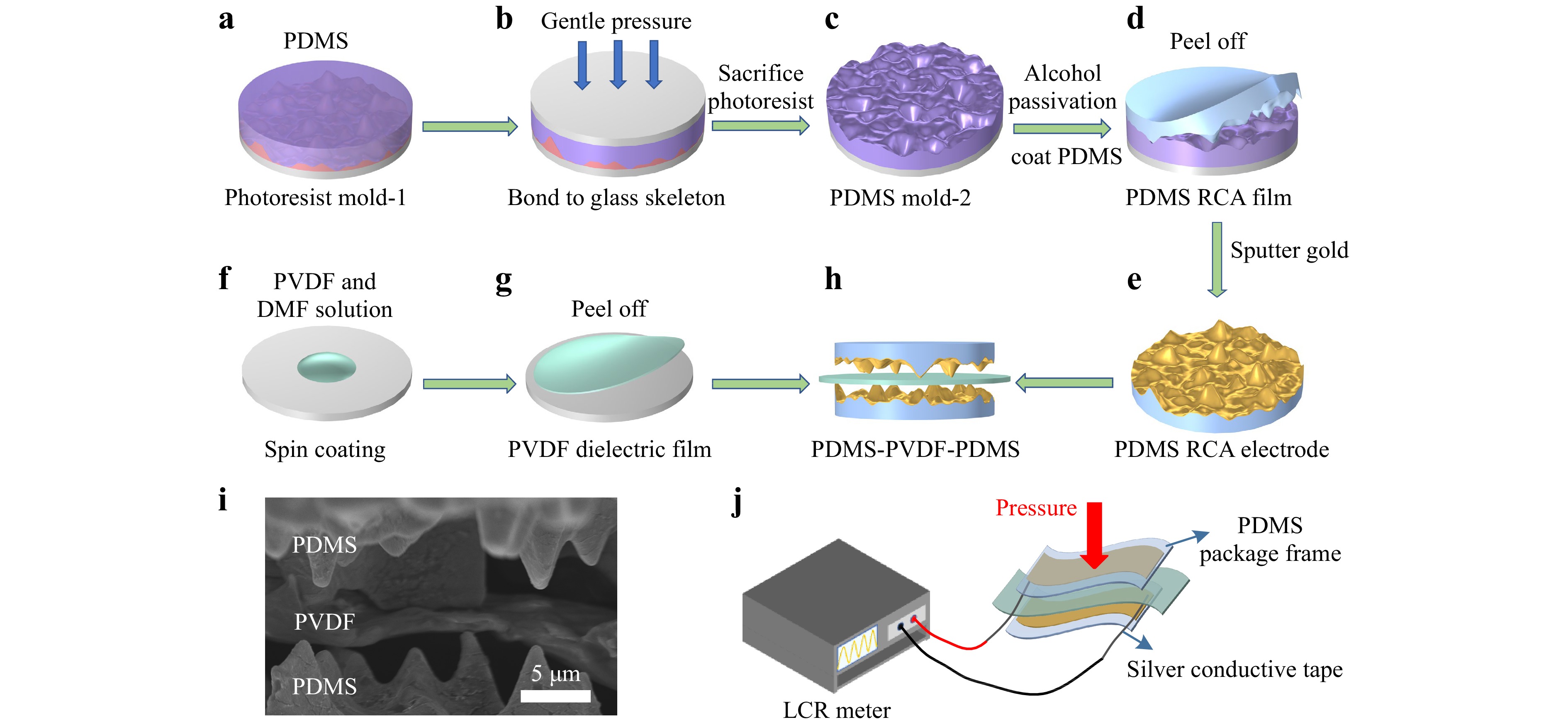
Fig. 4 Preparation of flexible capacitive pressure sensors. a Spin-coating of the PDMS mixture on photoresist mold-1. b Glass sheet coated with a thin PDMS layer placed and gently pressed on the uncured PDMS. c Combination in b, placed in an ethanol solution with the photoresist sacrificed to release the PDMS mold-2. d PDMS mixture coated on the PDMS mold-2 after alcohol passivation, and peeling of PDMS RCA film after curing. e Gold sputtered on the PDMS RCA film for fabricating the RCA electrode. f PVDF and DMF solution spin-coated on the wafer. g PVDF dielectric film peeled off after annealing curing. h Assembly of the PDMS–PVDF–PDMS sandwich structure. i Scanning electron microscopy (SEM) image of the PDMS–PVDF–PDMS sandwich structure in a close-contact state. j Integrated structure diagram and pressure measurement method of the capacitive pressure sensor.
First, the PDMS prepolymer and curing agent (Dow Corning, Sylgard 184) were mixed in a mass ratio of 10:1. The mixture was stirred at 500 rpm for 30 min using a magnetic stirrer to obtain a homogeneous PDMS blend. Subsequently, the bubbles in the PDMS mixture were eliminated using a vacuum rev-rot gravity mixer (Sinomix, VM300SA2), and it was spin-coated on the photoresist mold-1 (Fig. 4a). The PDMS-coated photoresist mold-1 was transferred to a hot plate and preheated at 80 °C for 5 min. When the PDMS mixture was partially cured, a clean, larger wafer was subjected to oxygen plasma treatment, followed by the spin-coating of a thin layer of the PDMS mixture on its surface. Thereafter, glass was gently pressed onto the PDMS layer and cured on a hot plate at 80 °C for 3 h (Fig. 4b). To transfer RCA microstructures from photoresist mold-1 with high fidelity, we employed a chemical method for the microstructure transfer process. After cooling, the assembly was immersed in anhydrous ethanol. Because SPR220-7 is soluble in anhydrous ethanol, PDMS mold-2 with a glass skeleton was released after the photoresist was dissolved (Fig. 4c). Notably, the dry PDMS mold-2 has long-term applications. Subsequently, a PDMS RCA film was prepared at the same PDMS mixing ratio. Because PDMS mold-2 must be demolded to peel the cured PDMS RCA film from its surface, a simple alcohol passivation method with good shape retention and durability was used for demolding35. PDMS mold-2 was treated with oxygen plasma, followed by immersion in a sealed Petri dish containing anhydrous ethanol for 30 min. Thereafter, it was transferred to a hot plate at 80 °C and dried for 30 min. Subsequently, the PDMS mixture was spin-coated on PDMS mold-2 at a rotational speed of 200 rpm for 30 s. The PDMS-coated PDMS mold-2 was cured in an oven at 80 °C for 2 h. Following cooling, the PDMS RCA film was gently peeled off (Fig. 4d) with a thickness of approximately 220 µm. Gold was sputtered onto the surface of the PDMS RCA film, resulting in a PDMS electrode with an RCA microstructure (Fig. 4e).
PVDF powder (Macklin, average Mw ~400,000) and N, N-dimethylformamide (Macklin, AR, 99.5% purity) were mixed at a mass ratio of 1:10. After thorough stirring, the solution was spin-coated onto clean glass and annealed at 80 °C for 30 min (Fig. 4f). After cooling, the PVDF dielectric film was gently peeled (Fig. 4g) to a thickness of approximately 2.5 µm. The electrode and dielectric layers were assembled in a sandwich structure using the PDMS–PVDF–PDMS configuration (Fig. 4h). Fig. 4i shows the cross section of the PDMS–PVDF–PDMS sandwich structure in a close-contact state. Silver conductive tape was used to connect the electrodes, resulting in a capacitive pressure sensor with RCA microstructured electrodes. Finally, two additional layers of PDMS frames were applied for the final packaging and further protection. The external frames were securely bonded to enhance sensor stability by subjecting each film to a simple oxygen plasma treatment. An electronic universal testing machine (Zhiqu, ZQ-990LB) was used to apply pressure on the sensor, and a precision LCR meter (Agilent, LCR-E4980A) was used to measure the real-time capacitance C. Fig. 4j shows the integrated packaged structure and pressure measurement method of the capacitive pressure sensor.
-
Various PDMS microstructured electrodes were fabricated under different conditions. Fig. 5a–c show the underexposed, normally exposed, and overexposed PDMS electrodes at the same one-dimensional speckle size of σ1 = 2.5 μm. Fig. 5d–f show the overexposed PDMS electrodes at σ2 = 5 μm, σ3 = 10 μm, and σ4 = 15 μm.
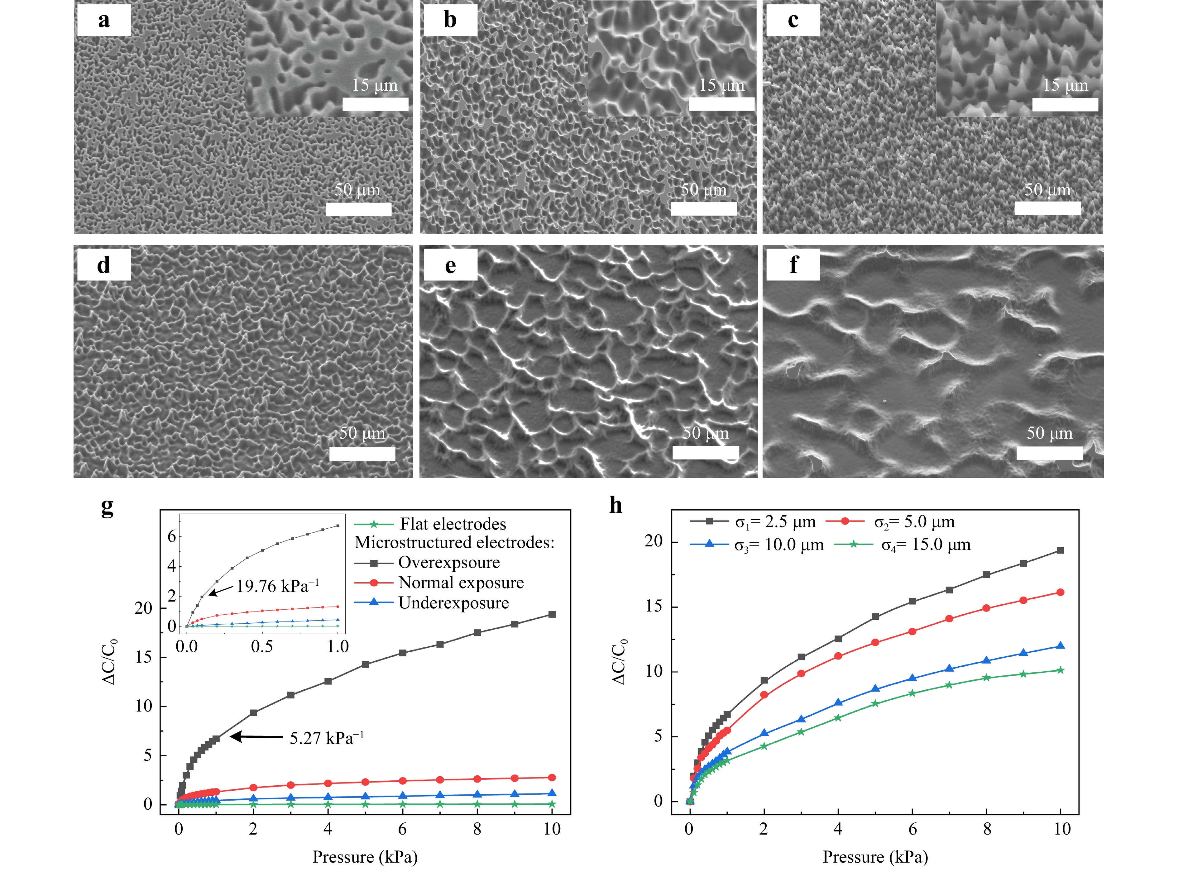
Fig. 5 SEM images of the PDMS microstructured electrodes and the sensitivities of the sensors. a–c SEM images of underexposed, normally exposed, and overexposed microstructured electrodes at the same one-dimensional speckle size of σ1 = 2.5 μm. Insets show the magnified SEM images. d–f SEM images of overexposed microstructured electrodes at σ2 = 5 μm, σ3 = 10 μm, and σ4 = 15 μm. g–h Relative capacitive variation-pressure curves of capacitive pressure sensors with different PDMS electrodes.
The sensitivity S of capacitive pressure sensors prepared under different conditions was tested using the formula S = (∆C/C0) /P, where ∆C = C – C0 and C and C0 represent the capacitances under P and zero pressure, respectively. As shown in Fig. 5g, the sensitivity of the sensor with flat electrodes was 0.03 kPa−1 for the pressure range of 0–1000 Pa. At σ1 = 2.5 μm, the sensors with underexposed and normally exposed microstructured electrodes exhibited sensitivities of 0.77 and 4.99 kPa−1 for the low-pressure range of 0–100 Pa, and sensitivities of 0.4 and 0.92 kPa−1 for the pressure range of 100–1000 Pa, respectively. At σ1 = 2.5 μm, the sensors with overexposed RCA microstructured electrodes exhibited an ultra-high sensitivity of 19.76 kPa−1 for the low-pressure range of 0–100 Pa, and a sensitivity of 5.27 kPa−1 for the pressure range of 100–1000 Pa. Further, as shown in Fig. 5h, the sensors with various overexposed RCA microstructured electrodes exhibited sensitivities of 19.76, 18.06, 12.2, and 6.7 kPa−1 for the low-pressure range of 0–100 Pa, and sensitivities of 5.27, 4.1, 2.92, and 2.75 kPa−1 for the pressure range of 100–1000 Pa at σ1 = 2.5 μm, σ2 = 5 μm, σ3 = 10 μm, and σ4 = 15 μm, respectively.
The sensing layer within the fabricated sensor can be flexibly divided into three regions: the upper and lower PDMS microstructured electrodes, PVDF dielectric film, and air gap. The capacitance C is expressed as C = ε0 (εpVp + εaVa) A/d, where ε0, εp, and εa denote the vacuum dielectric constant and the relative dielectric constants of PVDF and the air gap, respectively, Vp and Va denote the volume proportions of PVDF and the air gap within the dielectric layer, respectively, A represents the overlapping area of the upper and lower electrodes, and d is the electrode spacing.
As the morphology of the PDMS microstructured electrodes was identical to that of the photoresist molds, the criteria for evaluating their morphologies were the same. In Fig. 5g, upon transitioning from underexposure to overexposure, the fill factors of the PDMS microstructured electrodes, prepared with a speckle size of 2.5 μm, gradually decreased to 93.38%, 78.76%, and 52.32%, i.e., the air gap within the microstructures was enlarged. The fill factor influences the equivalent Young’s modulus Ee and equivalent dielectric constant εe. Because air cannot provide effective deformation resistance, it reduces the Ee of the microstructures, i.e., the fill factor is directly proportional to Ee. According to the elastic deformation formula Ee = F/∆d, Ee is inversely proportional to the deformation variable ∆d of the elastic body at constant stress F. Hence, the elastic body is easily compressible, i.e., the decrease in d is more significant. The decreasing fill factor increases Va and decreases Vp based on εe = εpVp + εaVa, resulting in a smaller εe. Therefore, a larger volume of air gap is occupied during deformation, resulting in a greater increase in εe. The synergistic effect of d and εe significantly varies the capacitance. Hence, owing to the small fill factor, the sensitivities of the sensors prepared under the four conditions for the electrodes (flat, underexposure, normal exposure, and overexposure) increase sequentially.
As shown in Fig. 5h, under the same overexposure conditions, the fill factors of the PDMS electrodes with RCA microstructures, prepared with speckle sizes of σ1 = 2.5 μm, σ2 = 5 μm, σ3 = 10 μm, and σ4 = 15 μm, were 52.32%, 48.66%, 51.02%, and 48.09%, respectively. Smaller speckle sizes yield finer and denser RCA microstructures. Choong et al.8 explained the shape factor of a microstructured elastomer as the ratio of the area to be compressed (e.g., the top of a cone) to the total unloaded surface area (e.g., the side of a cone) for free expansion. Huang et al.36 stated that a small shape factor promotes microstructural deformation. The microstructures were analyzed collectively owing to their randomness. The total compressed area was represented by the fill factor. Because the fill factors of these different RCA microstructures were similar, their total compressed areas were approximated to be the same. Subsequently, the finer and denser RCA microstructures had larger total unloaded side areas, resulting in smaller shape factors. In their study on diverse bionic microstructures, Tang et al.37 remarked that fine, high-density surface microstructures are more prone to deformation under external loads. Therefore, fine and dense RCA microstructures become more prone to deformation as the speckle size decreases gradually, resulting in significant capacitance variations and increased sensitivity of the sensor.
Furthermore, the response time of the sensor was tested, and the subsequent tests were performed using the capacitive pressure sensor with an ultra-high sensitivity of 19.76 kPa−1 (0–100 Pa). When subjected to loading and unloading pressures of 1 kPa, the sensor exhibited short response times of 131 and 133 ms, respectively, as shown in Fig. 6a. Fig. 6b shows the relative capacitive variation when a static pressure of 1.9 Pa was applied to the sensor, indicating that the sensor can detect subtle stimuli. In particular, the pressure was applied by placing a 6 mm × 6 mm plastic film on the sensor with a mass of ~6.86 mg. To test the consistency of the sensor, were applied sequentially pressures of 0.2, 0.5, 1.0, 3.0, and 10.0 kPa to it, and five cycles were performed at each pressure level. Fig. 6c shows that the sensor exhibited the same relative capacitive variation for the same load and returned to its initial state after multiple loading and unloading cycles, thereby demonstrating excellent consistency. To test the fatigue and durability of the sensor, we subjected it to more than 10,000 cycles at 8 kPa. Fig. 6d shows the sensor response during the compression test, highlighting the responses during the 2000–2010th, 5000–5010th, and 8000–8010th cycles. The sensor demonstrated remarkable stability and consistency over at least 10,000 pressure cycles, indicating excellent durability with no signs of fatigue. Therefore, a sensor with an RCA microstructured electrode offers high sensitivity, precision, stability, and durability.
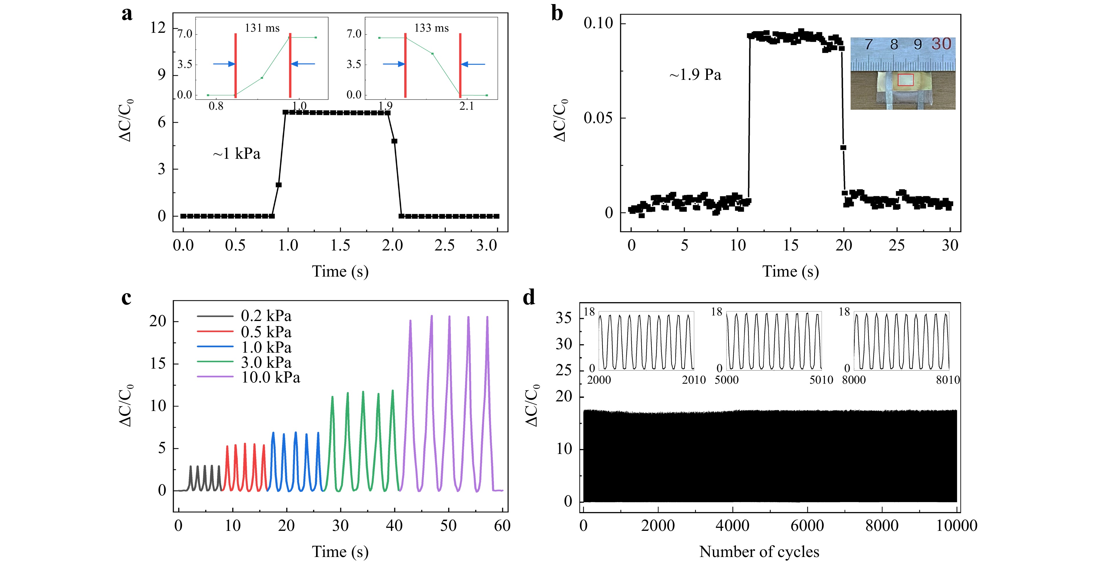
Fig. 6 Other performance testing of the sensors. a Response time of loading and unloading. b–c Relative capacitive variation–time curve for detecting ultralow pressure and five cycles per pressure at varying pressures. d Sensor stability test in over 10,000 cycles of compression, and the inset shows the relative capacitance variation curves at different stages of the cycle.
Subsequently, the practical applications of the sensor were investigated. As shown in Fig. 7a (relative capacitive variation: 0–0.05), the sensor was placed on the upper lip to capture subtle pressure signals caused by airflow disturbances during nasal breathing to monitor respiratory rate. This has significant implications for respiratory and pulmonary diseases such as asthma and pneumonia. Based on the relative capacitive variation–time curves, the breathing rate of the subjects was 16 breaths per minute under relaxed conditions, which was within the normal range.
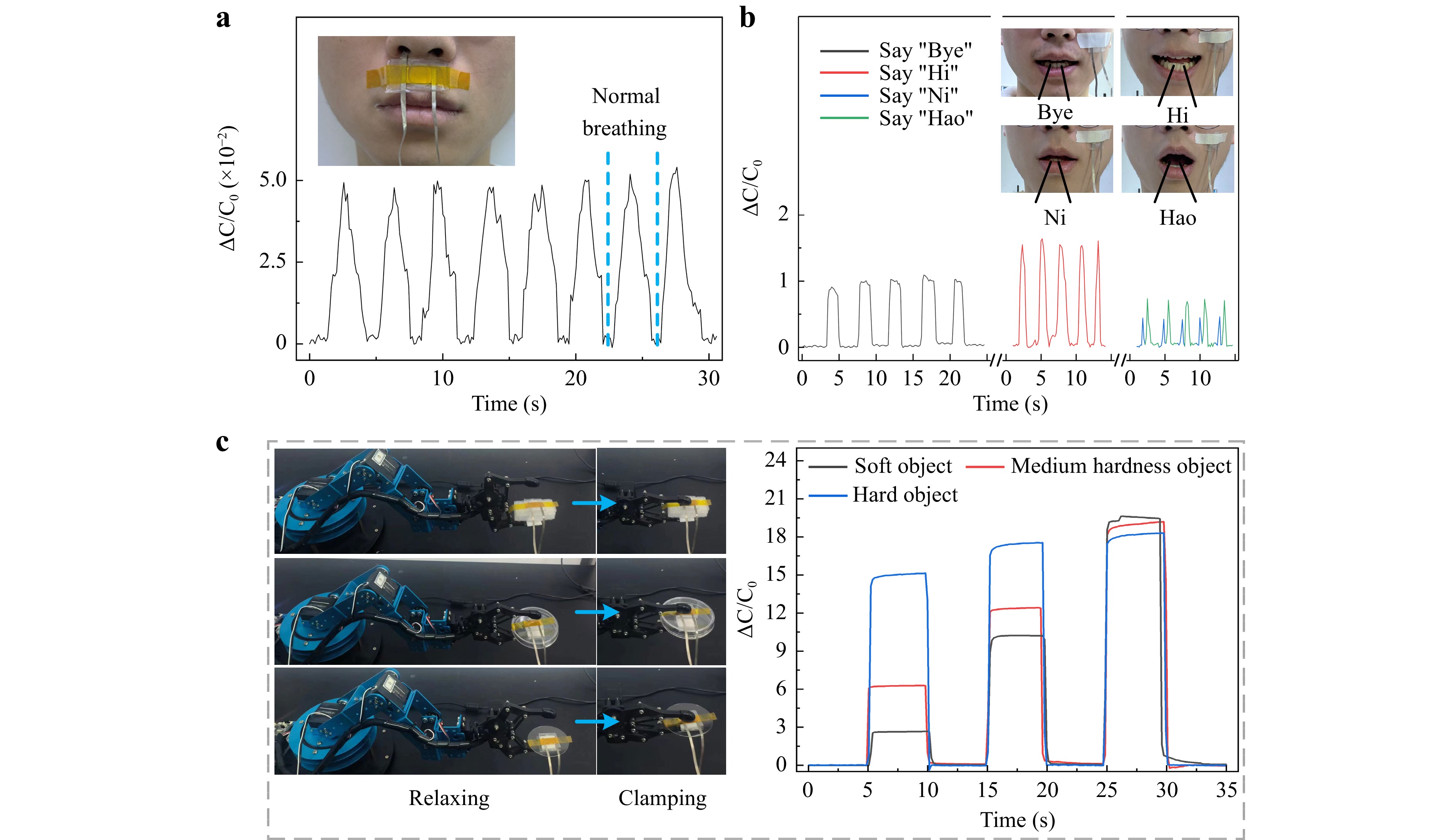
Fig. 7 Practical application of the sensors. a Sensor attached to the upper lip to capture respiratory rate signals. b Sensor positioned on the cheek to detect subtle facial expression signals. c Sensors affixed to the surfaces of sponges, plastic boxes, and glass. These were grasped by a robotic arm to gauge their respective softness or rigidity.
A sensor was placed on the cheek to detect subtle facial expressions based on muscle changes. We used a simple method of having a participant say “Bye,” “Hi,” and “Ni Hao” to induce different facial muscle movements. Five cycles were performed for different words, as depicted in Fig. 7b (relative capacitive variations: 0–1.54). For saying “Bye,” “Hi,” “Ni,” and “Hao,” the average amplitudes (relative capacitive variation) were 0.91, 1.54, 0.44, and 0.74, the time intervals were 4.32, 2.22, 2.35, and 2.35 s, and the durations were 2, 1.04, 0.39, and 0.52 s, respectively. Thus, speaking different words in different ways resulted in distinct signal waveforms. As shown in the figure, uttering different words involves varying facial muscle movements, resulting in different signal amplitudes. Deliberate control of the speech rate can alter the waveform frequency, for instance, repeating “Hi” or “Ni Hao” rapidly and “Bye” slowly. In addition, the extended duration of each saying “Bye” maintained facial movements, causing the signal to broaden. The flexibility, low detection limit, and fast response time of the sensor enable accurate identification of the words “Ni” and “Hao” when pronounced rapidly, underscoring its potential for capturing subtle and rapid facial movements.
To assess its tactile potential, we attached the sensor to the surfaces of objects of varying hardness, such as sponges, plastic boxes, and glass, which were clamped using a robotic arm. Fig. 7c shows the relative capacitive variation–time curves of the three test objects during the clamping–relaxation process. The upper and lower slopes of the curves represent clamping and relaxation processes, respectively. The output torque of the robotic arm motor was controlled using a computer, and three successively increasing clamping levels were applied to the objects. The variations in the motor output torque corresponding to the adjacent clamping levels were equal. The arm held each object at the three clamping levels for 5 s and then relaxed. Soft objects were deformed when the robotic arm was clamped. Based on the deformation relationship, the object primarily absorbs the load from the robotic arm, thereby reducing the pressure experienced by the sensor. However, hard objects are not easily deformed and the robotic arm load acts directly on the sensor, thereby increasing the pressure experienced by the sensor. Therefore, during the primary and secondary levels of clamping, the softer the object, the smaller the relative capacitive variation feedback from the sensor. However, when mechanical clamping was significant, the soft objects were less susceptible to deformation post-compression, enabling their sensors to detect high pressures. Therefore, the sensors on the three tested objects were under high pressure at the maximum clamping level and exhibited similar and larger relative capacitive variations.
These results indicate that the capacitive pressure sensor with an RCA microstructured electrode exhibits outstanding performance and has application potential for medical monitoring and robotics.
The impact of external environmental factors such as humidity and temperature on the static performance of the sensor was further explored (see Figs. S2a and b in Supplementary Information). The sensor was virtually unaffected by humidity owing to the additional protective encapsulation and waterproof property of PDMS38; however, with the changes in temperature ranging from -9 to 53 °C, the relative capacitive variation of the sensor decreased by approximately 0.1 because of the thermal expansions of the PDMS electrodes and PVDF dielectric film. In addition, the impact of mechanical deformation on the sensor was investigated (see Figs. S2c–e in Supplementary Information). Larger deformations, such as in-plane stretching, out-of-plane bending, and twisting, resulted in greater relative capacitive variations. To decouple the sensor responses to pressure and strain, future research can study this strategy further by positioning identical sensing units in an array at different locations39,40. By analyzing the force-coupling relationships in different directions of the sensor array, the force-coupling synergy relationships in each direction can be obtained, and the forces applied in different directions can be analyzed and decoupled40. Finally, Table 1 presents a performance comparison between the capacitive pressure sensor developed in this study and other capacitive pressure sensors with micropatterns. In this study, the sensor demonstrated significant sensitivity at low pressures compared with the sensors reported in Refs. 18–26. Additionally, it exhibited an excellent detection limit and stability.
Microstructure Material Sensitivity
(kPa−1)Detection limit
(Pa)Detection range
(kPa)Stability cycles Reference Microcylinder PDMS 5 0.11 <5 10000 18 Tilted micropillar PDMS 0.42 1 <1.5 1000 19 Microdome PDMS 0.0044 55 <11 1000 20 Microsphere PDMS 1.807 — <0.05 1000 21 Micropyramid Ecoflex 2.51 2.0 <2.5 5000 22 Microcone PDMS 4.99 — <0.2 5000 23 Micro cylindrical ladder PDMS 0.12 20 <1 409 24 Microtower PDMS 1.2 0.8 <2 100000 25 Microcone arrays Thermo-
plastic poly-urethane0.11 20 <20 4000 26 RCA PDMS 19.76 1.9 <0.1 10000 This study 5.27 0.1–1 Table 1. Sensor performance comparison
-
We leveraged the autocorrelation function of the laser speckle intensity, which follows a first-order Bessel function of the first kind. By optimizing the speckle size and exposure dose, we obtained a detailed spatial distribution of the speckle intensity on the low-contrast photoresist SPR220-7. This groundwork enabled us to perform grayscale lithography on laser speckles. Compared with our previous study, building on this grayscale lithography, we fully utilized the characteristics of laser speckle patterns and relatively easily crafted RCA microstructures. These microstructures were subsequently integrated into flexible capacitive pressure sensors. Compared with other methods, such as DMD-based grayscale lithography, the process of creating these cone-like microstructures through laser speckle grayscale lithography has proven to be both straightforward and reliable. Notably, these sensors exhibit high precision when monitoring physiological and tactile signals. Their outstanding stability, durability, and accuracy highlight their potential applications in medical monitoring and robotics.
In future research, we plan to combine RCA microstructures prepared using laser speckle grayscale lithography with ionic gels41,42. This combination is expected to aid in the fabrication of iontronic pressure sensors, contributing to achieving a much higher sensitivity because of the associated electron double layer effect42. We also plan to design functional circuits and integrate them with a standalone stretchable device platform to assist flexible sensors in adapting to intricate surfaces and achieving wireless perception43-45. Finally, using a self-powered triboelectric nanogenerator, we expect that sensors can operate properly when power or electricity is disrupted/unavailable46,47.
RCA microstructures prepared using laser speckle grayscale lithography can also be used in other potential applications. For example, they can be used to improve the performance of optical and electro-optical devices because they exhibit excellent anti-reflection performance48. They can also be applied for continuous and efficient fog collection because the conical structure can considerably improve the transportation efficiency of water droplets on the surface and even cause water droplets to resist gravity49. Finally, they can be applied to patches that promote wound healing because the conical microstructures can easily penetrate the skin, effectively deliver drugs to the target area, and maintain the local drug concentration for a long time50.
-
This work was supported by the Key Research and Development Program of Shanxi Province (202102030201002); the Changjiang Scholars and Innovative Research Team at the University of Ministry of Education of China (IRT_17R70); the State Key Program of National Natural Science of China (11434007); the 111 Project (D18001); the Fund for Shanxi “1331 Project” Key Subjects Construction.
Laser speckle grayscale lithography: a new tool for fabricating highly sensitive flexible capacitive pressure sensors
- Yong Zhou1, 2,
- Kun Wang1, 2,
- Junkun Mao1, 2,
- Yifei Ma1, 2,
- Mei Wang1, 2,
- Suotang Jia1, 2,
- Xuyuan Chen1, 2,
-
Zhaomin Tong1, 2, *, ,

- Light: Advanced Manufacturing , Article number: (2024)
- Received: 20 November 2023
- Revised: 06 March 2024
- Accepted: 12 March 2024 Published online: 05 June 2024
doi: https://doi.org/10.37188/lam.2024.016
Abstract: Achieving a high sensitivity for practical applications has always been one of the main developmental directions for wearable flexible pressure sensors. This paper introduces a laser speckle grayscale lithography system and a novel method for fabricating random conical array microstructures using grainy laser speckle patterns. Its feasibility is attributed to the autocorrelation function of the laser speckle intensity, which adheres to a first-order Bessel function of the first kind. Through objective speckle size and exposure dose manipulations, we developed a microstructured photoresist with various micromorphologies. These microstructures were used to form polydimethylsiloxane microstructured electrodes that were used in flexible capacitive pressure sensors. These sensors exhibited an ultra-high sensitivity: 19.76 kPa−1 for the low-pressure range of 0–100 Pa. Their minimum detection threshold was 1.9 Pa, and they maintained stability and resilience over 10,000 test cycles. These sensors proved to be adept at capturing physiological signals and providing tactile feedback, thereby emphasizing their practical value.
Research Summary
Laser speckle grayscale lithography for fabricating highly sensitive pressure sensors
Achieving high sensitivity for practical applications has always been one of the main developmental directions for wearable flexible pressure sensors. Zhao-min Tong from China’s Shanxi University and colleagues now report a laser speckle grayscale lithography system and a novel method for fabricating random conical array (RCA) microstructures using grainy laser speckle patterns. Its feasibility is attributed to the autocorrelation function of the laser speckle intensity, which adheres to a first-order Bessel function of the first kind. These RCA microstructures were used to form polydimethylsiloxane microstructured electrodes that were used in flexible capacitive pressure sensors. These sensors exhibited ultra-high sensitivity: 19.76 kPa-1 for the low-pressure range of 0–100 Pa. The team demonstrated several applications of these sensors, including their ability to capture physiological signals and provide tactile feedback.
Rights and permissions
Open Access This article is licensed under a Creative Commons Attribution 4.0 International License, which permits use, sharing, adaptation, distribution and reproduction in any medium or format, as long as you give appropriate credit to the original author(s) and the source, provide a link to the Creative Commons license, and indicate if changes were made. The images or other third party material in this article are included in the article′s Creative Commons license, unless indicated otherwise in a credit line to the material. If material is not included in the article′s Creative Commons license and your intended use is not permitted by statutory regulation or exceeds the permitted use, you will need to obtain permission directly from the copyright holder. To view a copy of this license, visit http://creativecommons.org/licenses/by/4.0/.

 DownLoad: