


-
Bessel beams, first proposed in 19871, represent a special class of exact solutions to the Helmholtz equation. Their radial intensity is proportional to the Bessel function of the first type, and they can propagate invariably over long distances. Bessel beams have gained significant attention in particle manipulation2,3, optical coherence tomography4,5, super-resolution microscopy6, and laser machining7,8 because of their long depth of focus, micron-sized spots, and self-reconstruction properties. To date, the experimental generation of quasi-Bessel beams featuring a finite radius and energy has mainly relied on the use of axicons, spatial light modulators (SLMs), and holographic metasurfaces9–11. However, these traditional methods are limited by bulky and expensive optical elements as well as complex manufacturing processes. Therefore, to meet the miniaturization demand for integrated optical systems, planar diffractive optical elements (DOEs), particularly binary optical elements (BOEs), are alternatives to refractive optics owing to their small volume, light weight, and compact configuration. Numerous optical functions can be realized through the precise design of the surface topographies of DOEs to obtain diffraction gratings, beam shapers, and focusing lenses12–14.
Currently, manufacturing technologies are limited by the tradeoff between overall size, throughput, and resolution. Considering that the wavefront modulation performance of BOEs is directly related to their surface relief profiles, achieving sufficient surface roughness for optical applications is indispensable. Consequently, the accuracy limit imposed by manufacturing techniques should be prioritized. Two-photon polymerization (2PP), initiated by a femtosecond laser, is a mask-less lithography technology with high precision15,16. It has a sub-wavelength direct writing resolution and complex three-dimensional (3D) structure manufacturing capability, enabling the fabrication of micro-optical elements with arbitrary 3D topography and remarkable optical quality. With the assistance of 2PP technology, the manufacture of Fresnel zone plates17, Dammann gratings18, and holograms12 has been reported. For further applications of Bessel beams in integrated optics, high quality diffractive phase plates that combine axicon and spiral phases have been fabricated with unique optical properties19. Recently, phase plates fabricated via the 2PP method have been demonstrated to generate Bessel beams of arbitrary order that have a ring-shaped vortex phase20. However, owing to the slow voxel-by-voxel scanning approach, the applicability of this method is restricted to small structures subject to a processing time of several hours per cubic millimeter. Although low-inertia galvanometric scanners can achieve high scanning speeds, the overall size of the fabricated structure is limited by the working area of the objective, which does not exceed hundreds of microns21. In addition, although combining spatial laser beam shaping with 2PP can significantly improve production efficiency, this approach is currently limited to the fabrication of microstructures with periodic22 or specific 3D shapes23–25; it has not been employed in printing BOEs with arbitrary surface relief profiles. Therefore, the fabrication of complicated BOEs as large as needed for functional applications without sacrificing contour fidelity has yet to be achieved.
In this regard, additive manufacturing methods, such as digital light processing (DLP) and stereolithography (SLA) are characterized by fast processing speeds and high efficiencies, rendering them feasible for performing batch fabrication26. However, these methods cannot fabricate structures with a resolution better than 25 µm27, which is insufficient to achieve surface roughness for optical use. Therefore, the combination of 2PP with other processing steps or methods comes into focus. Several hybrid laser processing methods have been proposed in which the overall structure is divided into two parts, high- and low-resolution components that are manufactured using different methods28,29. However, alignment errors or surface quality degradation in the low-resolution parts result in additional scattering and weak points, thus, affecting the optical performance of BOEs. Repetitive scanning can be applied to improve surface quality; however, this extends the processing time.
Another factor affecting the size expansion is the strict height constraints imposed on BOEs. As BOEs utilize surface relief profiles to modulate the diffraction of light, and the local phase is determined by the corresponding structural height, a slight error will affect the final wavefront shaping performance. The femtosecond laser direct writing (FLDW) strategy typically requires tightly focused beams with large numerical apertures (NA). In this case, precise positioning of the sample with respect to the incident beam waist becomes critical because the Rayleigh range is of the order of the spot radius30. This critical positioning constraint renders ensuring that the height is equal to the theoretical value challenging. A common solution involves printing a base layer of thickness 1–2 μm to actively compensate for sample tilt and surface defects17,18. For mesoscale samples, it can be anticipated that the defects caused by positioning errors will become more severe.
In this study, we introduce a phase-only SLM into a conventional 2PP system to actively extend the focal depth of a tightly focused spot along the beam propagation direction without significantly sacrificing the numerical aperture. The on-axis intensity of beams with a long depth of focus (LDoF) can exceed the polymerization threshold over a sufficiently long range to obtain high-aspect-ratio voxels. Therefore, for BOEs, the serial nature of 2PP fabrication can evolve into single-layer manufacturing, which exponentially reduces the processing time while maintaining microscale resolution. The extended focal depth also significantly reduced the sample positioning constraints. Thus, a base layer is not required to achieve a precise height because the sample fluctuation can be easily controlled within the depth of focus. Notably, with the aid of a linear stage, the overall size of the manufactured BOE can reach the mesoscale without an additional active focusing system or active compensation for substrate tilting. We designed a binary diffractive axicon with geometry comprising concentric rings with a constant pitch. The structure does not require to be divided and stitched; hence, the fabricated binary axicon of diameter 2.2 mm exhibits excellent surface flatness and optical performance. Under the illumination of Gaussian beams with a central wavelength of 1030 nm, emergent beams with a typical Bessel function intensity profile were observed and evaluated. Furthermore, to verify that the assembled Bessel lens was capable of wide-area processing, we ablated a gold film deposited on a silicon wafer to form excitation units of terahertz (THz) surface plasmon polaritons (SPPs). The near-field optical detection results demonstrate that a compact Bessel lens with BOE as the core element is feasible for FLDW processing over large samples.
-
Fig. 1a shows a schematic of the SLM-based femtosecond laser two-photon lithography system. The laser source was a custom designed femtosecond amplification system that generated 90 fs transform-limited pulses with a repetition rate of 1 MHz. The second harmonic wave generated by the β-barium borate (BBO) crystal (centered at 525 nm) was expanded to a width of ~8 mm to illuminate the SLM (Holoeye PLUTO, 1920 × 1080 pixels), which matched the active area size of the screen. The spatial intensity distribution characteristics of the LDoF beams were determined using a dynamic phase mask loaded onto the SLM, as shown in Fig. 1b. The phase mask is a superposition of two parts: the phases of the LDoF beams and the blazed grating (BG). The BG is employed to diffract the reproduced image to the -1st order such that the zeroth-order diffracted light caused by the defect of the SLM pixelated structure can be filtered with an iris. A lens (L, f = 1m) and a microscope objective (MO, Olympus 20×, NA = 0.4) comprise the 4-f system, which scales and relays the modulated beam into the photoresist (MicroChem, SU-8 2002). A neutral-density (ND) filter controls the pulse energy used for exposure. As shown in Fig. 1c, the LDoF beam was reconstructed at the back focal plane of the MO; this initiates polymerization within the blue dashed box. By modulating the phase mask, we ensured that the LDoF beams penetrated the full thickness of the photoresist layer. The combination of the exposure of the LDoF beams with the movement of the high-precision X-Y displacement stage enables the parallel precise direct writing of complex microstructures.
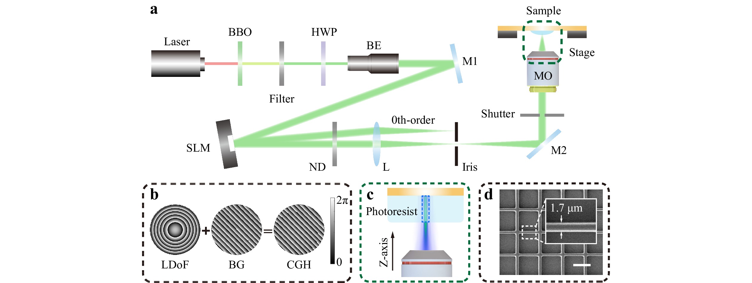
Fig. 1 a Schematic of the spatial light modulator (SLM)-based two-photon polymerization (2PP) system. HWP, half-wave plate; BE, beam expander; M1 and M2, mirrors; SLM, spatial light modulator; ND, neutral density filter; L, lens; MO, microscope objective. b Illustration of the phase mask loaded on the SLM, comprising the phase of LDoF beams and a blazed grating. c Partial enlargement of the focal region, showing the relative position of the LDoF beams and the photoresist. The blue dashed box indicates the region where two-photon absorption occurs. d Scanning electron microscopy (SEM) image of the crisscross structure. Scale bar = 10 μm.
Before manufacturing the binary optical elements, we fabricated a series of crisscross structures using the SU-8 2002. Fig. 1d shows a scanning electron microscopy (SEM) image of the microstructure after development. Under a scan speed of 170 μm/s and a single pulse energy of 1.5 nJ, the line width is measured to be approximately 1.7 μm, which provides a quantitative indicator for the feature size of LDoF beams direct writing.
-
Owing to the flexibility of the adaptive phase modulation of the SLM, the focusing characteristics of LDoF beams can be modified easily. By loading the axilens hologram onto the SLM, laser beams with different radii can be focused at different positions and a long focal depth can be generated. The phase distribution with a wavelength λ can be written as31
$$ \varphi (r) = \frac{{\pi {r^2}}}{{\lambda \left({f_0} + \dfrac{{\Delta z}}{{{R^2}}}{r^2}\right)}} $$ (1) where r is the radial coordinate, f0 is the focal distance, Δz is the focal length, and R is the radius of the diffraction plane. Here, aiming at improving the manufacturing throughput while maintaining the desired spatial resolution and feature definition, we select the hologram parameters as f0 = 2 m and Δz = 0.5 m. Scaled down by the 4-f system, the resulting numerical and experimental results of the intensity profile of LDoF beams are shown in Fig. 2, exhibiting high consistency. Fig. 2a, b show the longitudinal intensity distribution along the z axis; the interval between the two orange dashed lines indicates where the intensity exceeds the polymerization threshold. In this longitudinal range, near-uniform polymerization was initiated. However, we simulated the longitudinal intensity distribution of Gaussian beams focused by a low-NA objective (NA = 0.25), as shown in the inset of Fig. 2a. A comparison of the white solid and dashed lines in Fig. 2a indicate that the corresponding range of the Gaussian beams is notably shortened compared to the LDoF beams, resulting in a more rigorous requirement for the flatness and precise positioning of the sample. Notably, the radial dimension of the Gaussian beams is similar to that of the LDoF beams, whose full width at half maximum (FWHM) is 1.085 μm; the FWHM of LDoF beams is approximately 1.235 μm, ensuring a sufficiently fine feature size. Fig. 2c, d show the radial intensity distribution at the focal plane.
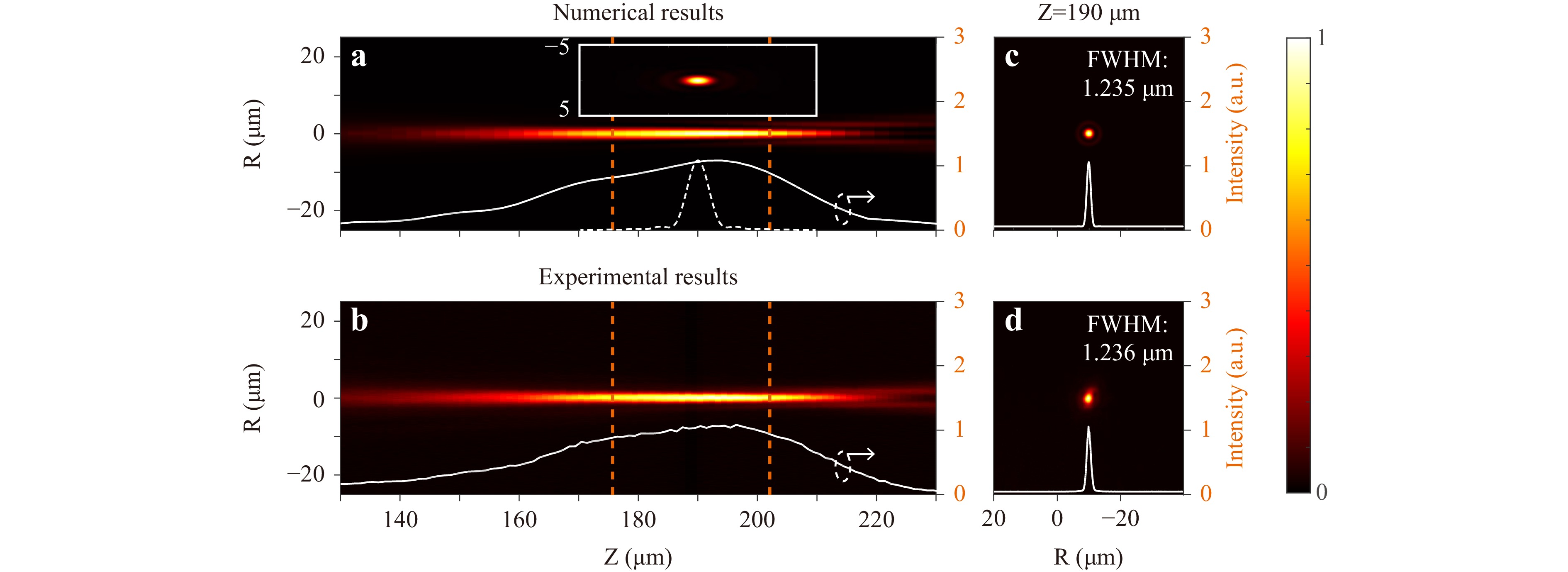
Fig. 2 Numerical and experimental intensity distribution of the LDoF beams. a, b Longitudinal intensity distribution of LDoF beams along the z-axis. The inset in a is the simulated longitudinal intensity distribution of the Gaussian beam focused by a microscope objective (NA = 0.25). The white solid and dashed lines represent the normalized intensity curves of LDoF and Gaussian beams at the center of the spots, respectively. c, d Radial intensity distribution at z = 190 μm.
-
Conventional axicons are refractive optical elements that convert an incident beam into a Bessel beam (Fig. 3a-1). They have rotational symmetry about the z-axis; their refractive properties are characterized by the base angle, α, and refractive index, n. Regarding the incident light as a class of rays parallel to the z-axis, they refract at the conical surface and cross the z-axis at the same angle θa. Considering Snell’s law and small angle approximation, θa is calculated to be

Fig. 3 Design of the binary diffractive axicon. a Illustration of the generation of quasi-Bessel beams by a-1 an axicon and a-2 a BOE. b Schematic of the transformation from a refractive axicon to a binary diffractive axicon.
$$ {\theta _a} = (n - 1)\alpha $$ (2) The non-diffracting propagation distance of the generated Bessel beam is related to the dimensions of the incident beam, which is expressed as
$$ {z_{\max }} = \frac{\rho }{{\tan {\theta _a}}} $$ (3) where ρ is the radius of the incident beam. Meanwhile, scalar diffraction theory views optical elements as infinitely thin surfaces; therefore, the transmission function of the axicons is calculated as
$$ T(R) = \exp \left[ {i{\varphi _m}\left( {1 - \frac{R}{{{r_a}}}} \right)} \right] $$ (4) where R is the radial coordinate and ra is the radius of the axicon aperture. φm represents the maximum phase shift that can be introduced:
$$ {\varphi _m} = (n - 1){r_a}\tan \alpha \cdot k $$ (5) where $k = 2\pi /\lambda $is the wave vector and λ is the wavelength. In response to the demand for miniaturization of optical systems, the principle of using a binary diffractive axicon to approximate a refractive axicon is shown in Fig. 3b. To significantly decrease the thickness, the optical path delay introduced by the refractive axicon was compressed to 0–λ. The resulting diffractive lens, also known as a kinoform lens, correspondingly introduces a phase shift varying continuously between 0 and 2π to the incident light. The transmission function is denoted by
$$ {T_{DOE}}(R) = \exp \left\{ {i \cdot \text{mod} \left[ {{\varphi _m}\left( {1 - \frac{R}{{{r_a}}}} \right),2\pi } \right]} \right\} $$ (6) For a kinoform lens, the maximum phase shift difference introduced by the material is 2π or integer multiples of it. At the pre-designed wavelength λ0, the thickness of the kinoform lens is defined by
$$ h = N \cdot \frac{{{\lambda _0}}}{{n - 1}} $$ (7) where N is a positive integer and n represents the refractive index of the photoresist.
However, the fabrication of continuous surface profiles remains challenging. To date, the manufacturing of kinoform lenses relies heavily on approximation32. Hence, it is necessary to use stepped phase profiles to approximate continuous relief structures, that is, BOEs proposed by Veldkamp et al.33. Assuming one phase step, the binarized phase profile of the diffractive axicon is shown in Fig. 3b, composed of a central disk and several concentric rings of the same height, h/2. Fig. 3a-2 shows a schematic of quasi-Bessel beams modulated by the BOE. The kth-order diffraction angle formed by the diffractive axicon can be expressed as34
$$ \sin {\theta _k} = k\frac{\lambda }{{2\Lambda }} $$ (8) where k = 1, 2, 3, … is the diffraction order and Λ is the pitch of concentric rings. Substituting θa in Eq. 2 with θk, the position where the kth-order diffracted beams intersect with the z-axis can be obtained as follows
$$ {z_k} = \frac{\rho }{{\tan {\theta _k}}} \approx \frac{{2\Lambda \rho }}{{k\lambda }} $$ (9) After the phase distribution of the axicons is binarized, the output consists of a superposition of several quasi-Bessel beams of different orders35. Higher orders correspond to smaller main-lobe sizes and shorter propagation distances. Therefore, interference among higher-order beams is inevitable, and has been demonstrated to cause intensity oscillations along the optical axis36. In regions where multiple beams coexist, tiny but intense spots or donut-shaped patterns appear owing to constructive or destructive interference between two Bessel-function electromagnetic fields, respectively.
-
Considering both the manufacturing accuracy of our 2PP setup and the application demands on the generated non-diffracting beams, we designed a binary axicon with a phase distribution as shown in Fig. 4a. The whole diameter is 2.2 mm, and the width of each concentric ring is 100 µm. The BOE is configured to work at a wavelength of 1030 nm, corresponding to a height of 2.78 µm that can induce a phase shift of 3π for the incident beam. The phase difference between two neighboring zones is set to 3π, not the commonly used π, corresponding to a tripled thickness as described in Eq. 7, because obtaining ultrathin layers of photoresist steadily via spin-coating is difficult. Considering that the support substrate will dominate the overall thickness of BOEs in all cases, the decrease in height of micro-structures from ~ 2λ to below λ may not be useful for most applications37. Therefore, we choose a photoresist thickness of 2.78 µm, which is easy to obtain by selecting an appropriate spin speed (850 revolutions per minute, rpm).
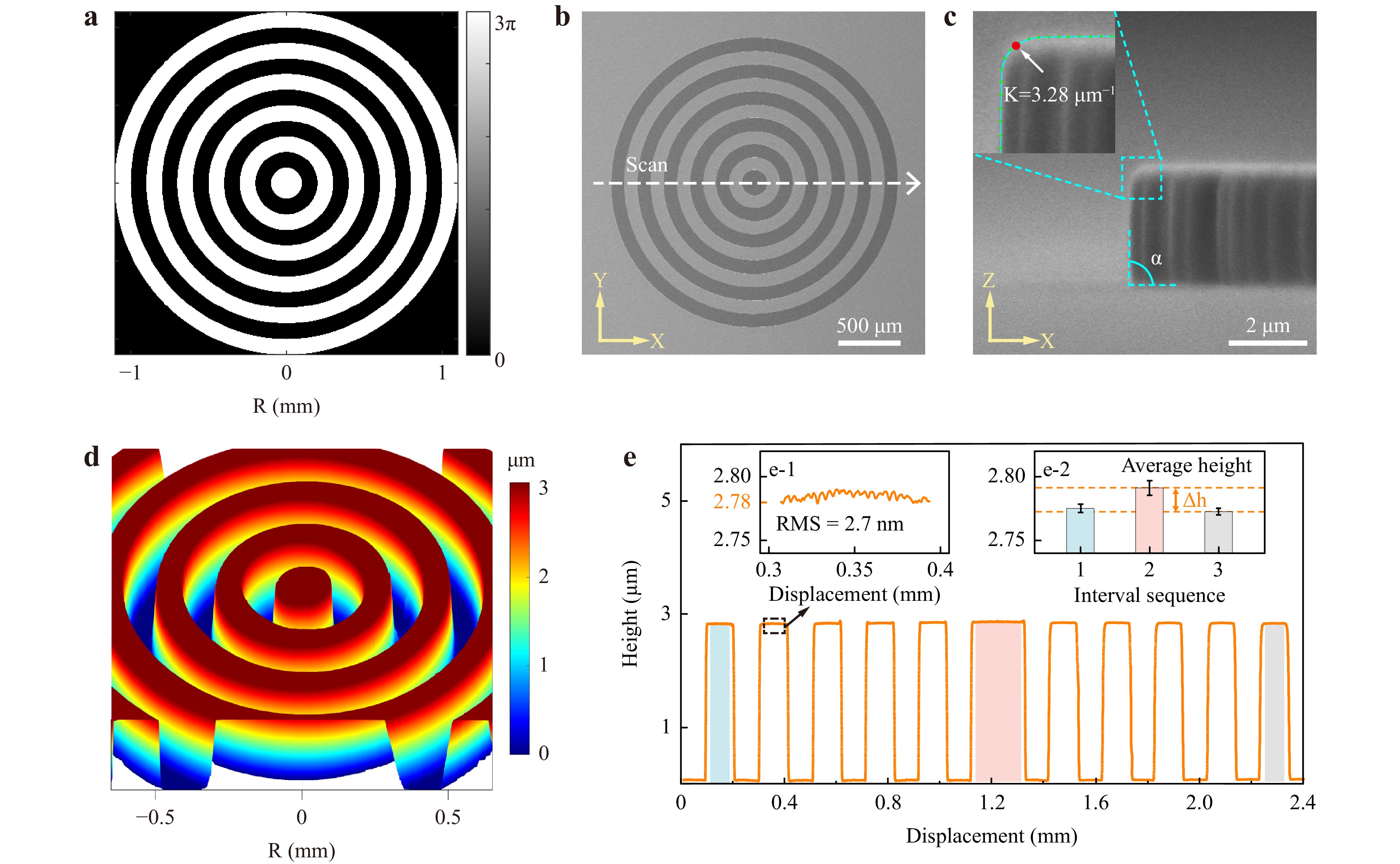
Fig. 4 3D morphology characterization of the binary diffractive axicon. a Phase distribution of the designed BOE. b Top view of the fabricated BOE under SEM. c Front view of the edge of BOE. The inset is a partial enlargement of the structure, and the cyan line represents the fitted edge curve. d Height profile of the BOE measured by the white light interferometer. e Precise height profile measured by the step meter. The scan direction is along the white dotted line in b. The inset e-1 is a partial enlargement of the height profile, corresponding to the black dashed line boxed area. The inset e-2 shows the average heights of the three colored intervals.
Using the femtosecond LDoF beam direct-writing method, we printed the designed binary axicon through single-layer scanning, and the exposure process was completed within 70 min. After laser processing, post-baking (95 ℃, 3 minutes), and developing, the as-formed structure is obtained on the substrate with high precision. The top view of the manufactured BOE under SEM is shown in Fig. 4b, and the front view of its edge is shown in Fig. 4c. The inset of Fig. 4c shows an enlarged view of the cyan dotted box, and the solid cyan curve is the fitted edge profile. We measured the curvature of the red dot, where K = 3.28 μm-1. This obtuse edge can be attributed to the inherent shrinkage of the SU-8 layer38 under surface tension. The edge steepness is characterized by measuring the angle α between the side wall and the substrate, where α = 89.65º. The height profile measured using a white-light interferometer is shown in Fig. 4d. Considering that height deviations have a significant impact on the BOE, we measured the precise surface profile using a step meter (Bruker DEKTAK XT) along the white dotted line in Fig. 4b. The profile in Fig. 4e shows that the height of the manufactured BOE is 2.78 μm, which is consistent with the designed value. The inset in Fig. 4e-1 shows a partial enlargement of the profile. The root mean square (RMS) was measured to be 2.7 nm, indicating the extremely low surface roughness of the structure. We calculated the average heights of the three colored intervals to further demonstrate the thickness uniformity of the BOE over a wide area. As shown in the inset Fig. 4e-2, the average heights are fairly close over a distance of ~2.2 mm, with a maximum height difference of Δh = 18.5 nm (~0.02π). In the absence of a base layer or fine focusing, the LDoF of the beams eliminated the effect of the slight tilt and irregularity of the sample on the height deviations. The topographies of the binary axicon exhibited high shape fidelity, indicating that our strategy has sufficient resolution and height controllability for fabricating binary optical elements on the millimeter scale.
-
A homemade Yb-doped fiber laser centered at a wavelength of 1030 nm was used to verify the performance of the binary diffractive axicon. Fig. 5a shows the optical system used for BOE characterization. An asymmetric 4-f system was introduced after the BOE to increase the power density of generated quasi-Bessel beams under the illumination of femtosecond Gaussian beams, we referred to this combination as a Bessel lens. The 4-f system consists of a 75 mm lens (L1) and a microscope objective (MO1, Olympus 50×, NA = 0.8), realizing proper scaling of both the spot size and the diffraction-free length of the quasi-Bessel beams, thus, matching the following microscopic imaging setup. The setup consisted of a 20× objective lens (MO2, Olympus, NA = 0.4), 200 mm lens (L2), and charge-coupled device (CCD). The magnification of the microscopic imaging system was determined by the spot size for a better representation of the CCD. A 20× objective lens was mounted on a motorized stage to complete scanning of the beam profile along the propagation direction. After measuring the intensity distribution on planes perpendicular to the optical axis using the CCD, the longitudinal intensity distribution can be calculated through post-processing.
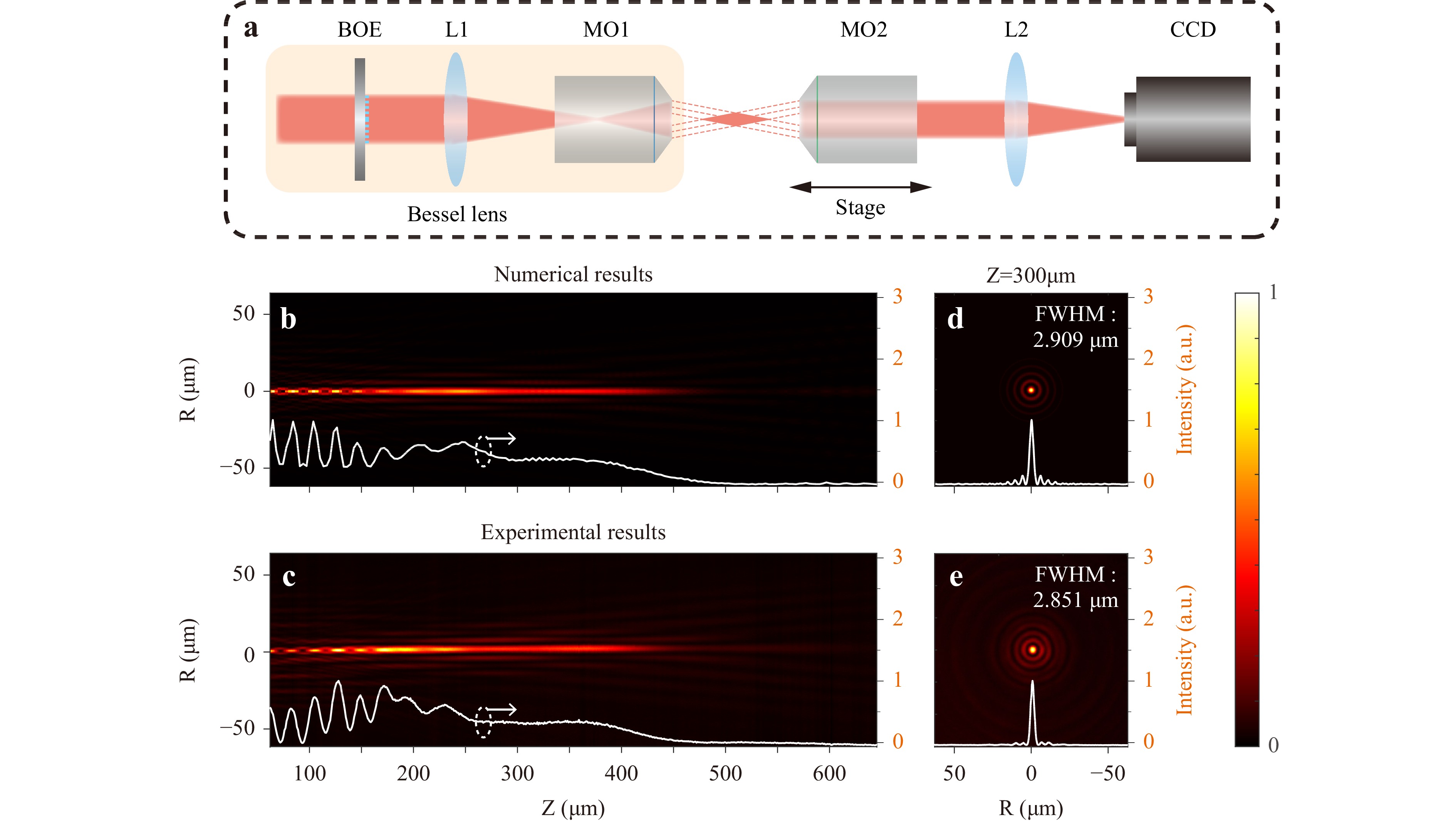
Fig. 5 Characterization of quasi-Bessel beams produced by the binary diffractive axicon. a Schematic of the microscopic imaging setup. b, c Numerical and experimental intensity distribution of the quasi-Bessel beams along the longitudinal direction. The white lines represent the normalized intensity curves at the center of the main-lobe. d, e Numerical and experimental radial intensity distribution at Z = 300 μm.
Figs. 5b–e compare the numerical results with the post-processed experimental results of the generated zeroth-order quasi-Bessel beams. As is shown in Fig. 5b, c, over the first 250 μm along the z-axis, the intensity oscillates with the propagation distance. This is attributed to the overlap between higher-order diffraction beams; the resulting interference modifies the shape of the non-diffracting beam. Two typical intensity patterns can be found, a small but intense spot and a donut-shaped one, indicating that the two interfering beams are in phase or out of phase, respectively. In the range 250–450 μm, the intensity and spot distributions of the zeroth-order Bessel beam remain essentially unchanged, demonstrating significant propagation invariance. The beams behave as expected over sufficiently long distances. Fig. 5d, e show the corresponding radial intensity distributions at Z = 300 µm. The radial intensity distribution has the typical characteristics of a zeroth-order Bessel beam featuring a bright central lobe surrounded by darker rings. The FWHMs of numerical and experimental results are also similar, which are 2.909 μm and 2.851 μm, respectively. We emphasize that the excellent agreement of intensity distributions in both longitudinal and radial directions between experimental and theoretical results indicates that LDoF beams assisted FLDW is a powerful method for the rapid and precise manufacture of BOEs.
-
The ultrafast pulse duration of the femtosecond laser minimizes the thermal effect when it interacts with materials, thereby facilitating a stable and reproducible machining process. Bessel beams are suitable for processing various materials because of their non-diffracting propagation properties, enabling the formation of high-aspect-ratio microstructures with sharp edges and overcoming the critical sample positioning for ultrafast laser surface nano-patterning30. To verify that the non-diffracting Bessel beams could enable the rapid inscription of microscale features over large sample areas, we used the Bessel lens shown in Fig. 6a to implement femtosecond laser ablation of periodic hole arrays on a gold film surface, which are available for coupling free-space THz radiation to excite SPPs. Considering the adequate length of the unchanged propagation region of zeroth-order Bessel beams, sample alignment and precise focusing during processing are significantly less critical, and the processing area is scalable to a large extent.
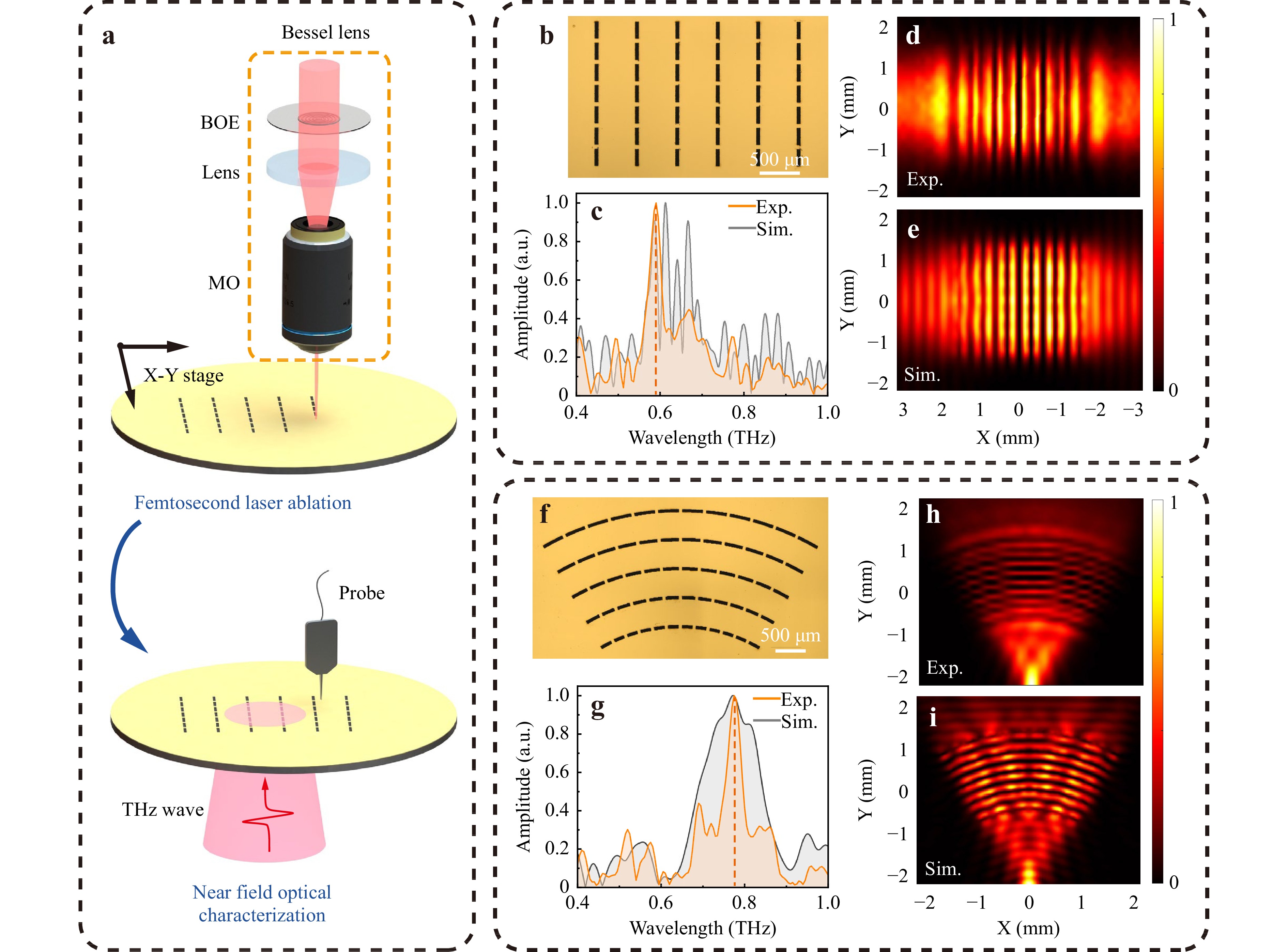
Fig. 6 a Schematic of the fabrication and characterization of the excitation unit. b, f Optical microscopic images of the ablated rectangular and arc-shaped areas. c, g Spectrums of the excited SPPs at typical points. The orange and gray curves represent the results of experiments and simulations, respectively. The orange dashed line indicates the spectrum peak. d, h Near-field images of the normalized power |Ez|2 distributions measured through SNTM system. e, i Simulated near-field images of the normalized power |Ez|2 distributions.
The femtosecond laser used for ablation is centered at 1030 nm with a pulse energy of 4 μJ, and a repetition rate of 50 kHz. The incident Gaussian beams were modulated and scaled down using a Bessel lens to obtain a higher power density that exceeded the ablation threshold of the sample. The sample was fabricated by magnetron sputtering a 200 nm-thick gold layer over high-resistivity silicon. By focusing on a sample placed on the 2D displacement stage, the quasi-Bessel beams selectively ablated and removed the gold film.
Periodic subwavelength hole arrays on metal surfaces can provide additional wave vector components39,40. As shown in the optical microscopic image in Fig. 6b, the area of the rectangular hole array is 2.5 mm × 1.75 mm. Each rectangular hole has a dimension of 200 μm × 40 μm and is arranged with a period of 485 μm and 250 μm along the x and y directions, respectively. In Fig. 6f, for the arc-shaped curved hole array, the innermost radius is 2.22 mm and the outermost radius is 3.82 mm, with a central angle of 60°. Curved holes with a width of 40 µm are arrayed with a period of 400 µm along the radial direction. Metal strips separating the hole arrays have a width of 50 µm and an angle of 5°.
Through a fiber-optic scanning near-field THz microscopy (SNTM) system, the ability of metal hole arrays to couple free-space THz radiation to SPPs is demonstrated. As shown in Fig. 6a, linearly polarized THz waves impinge on the excitation area from the bottom surface, whose direction is perpendicular to the hole gratings, to satisfy the excitation conditions. A Z-probe with a resolution of 8 μm is placed above the sample to detect excited SPPs, moving along the x and y directions with a step of 100 µm to complete the scanning of the signal.
We utilized the commercial software package CST Microwave Studio for modeling and simulation. At typical positions where the electric field power reached a maximum, we extracted the spectra of SPPs excited by rectangular and arc-shaped metal hole arrays, as shown in Fig. 6c, g. The spectral peaks of the two excitation regions appear at 0.59 THz and 0.78 THz, respectively. The actual positions of the spectrum peaks were consistent with the simulated ones, and the slight difference in the spectra may be attributed to geometric errors of the structure.
The near-field images in Figs. 6d, e, h, and i further demonstrate the ability of the hole arrays to excite SPPs. The electric near-field of the SPPs was visualized by plotting the normalized power |Ez|2 distributions as a 2D color map at the considered frequency. Figs. 6d, f and 6h, i show the SPP field distributions on the rectangular and arc-shaped excitation regions at 0.59 THz and 0.78 THz, respectively. The experimental results were in good agreement with the simulation results, demonstrating the reliability of the ablation method. Characterization using the SNTM system demonstrates that the ablated structures have well-defined surface morphologies; this confirms that the Bessel lens manufactured through our holographic FLDW method is suitable for femtosecond laser ablation over large samples and that the critical positioning constraint of the sample can be largely overcome with the aid of non-diffracting beams.
-
In this study, we report an FLDW method for the precise and rapid fabrication of mesoscale binary optical elements with microscale characteristics. The throughput improved exponentially while maintaining a fine feature size by substituting point-by-point scanning with one-layer scanning of the LDoF beams. We emphasize that the height of the manufactured BOE is equal to the theoretical value with an extremely low surface roughness, which is essential for phase-type DOEs. Meanwhile, the long focal depth overcomes the challenge of sample positioning, which enables direct writing over large areas and increases the overall dimensions without sacrificing processing accuracy. We fabricated a binary diffractive axicon with a diameter of 2.2 mm and a height of 2.78 μm, generating zeroth-order quasi-Bessel beams in high agreement with theoretical simulations. Thereafter, a Bessel lens is derived by combining the BOE with a 4-f system; the obtained non-diffracting beams are promising candidates for wide-area processing. Assuming THz SPPs excitation units as an example, we demonstrate the rapid and robust femtosecond laser ablation of metal films. These beams may have applications in optical manipulation, microscopic imaging, or FLDW41,42. Overall, the proposed LDoF-beam-assisted FLDW is a promising method for the high-throughput manufacturing of mesoscale BOEs with high profile fidelity, which is crucial for various fields dependent on the on-demand fabrication of functional integrated optical elements.
-
This work was supported by the National Natural Science Foundation of China (62227821), Shanghai Institute of Optics and Fine Mechanics, and Chinese Academy of Sciences (Open Fund of the State Key Laboratory of High Field Laser Physics). We thank the Shiyanjia Lab for supporting the SEM tests in this study (www.shiyanjia.com).
High throughput direct writing of a mesoscale binary optical element by femtosecond long focal depth beams
-
Yue Yang
 ,
, - Erse Jia,
- Xinyu Ma,
- Chen Xie,
- Bowen Liu,
- Yanfeng Li,
-
Minglie Hu*, ,
- Light: Advanced Manufacturing 4, Article number: (2023)
- Received: 19 June 2023
- Revised: 27 November 2023
- Accepted: 29 November 2023 Published online: 17 December 2023
doi: https://doi.org/10.37188/lam.2023.042
Abstract: Bessel beams have multiple applications owing to their propagation-invariant properties, including particle trapping, optical coherence tomography, and material processing. However, traditional Bessel-beam shaping techniques require bulky components, which limits the development of miniaturized optical systems for integration with other devices. Here, we report a novel femtosecond laser direct writing strategy for fabricating mesoscale (from submicrometer to subcentimeter) binary optical elements with microscale resolution. This strategy utilizes femtosecond beams with a long focal depth to increase throughput while reducing the constraints on critical sample positioning. As a demonstration, we manufactured and characterized a 2.2 mm diameter binary axicon. The experimentally measured quasi-Bessel beam intensity distribution and the numerical results were remarkably consistent, demonstrating a suitable tradeoff between the overall size, efficiency, and structural fidelity. Furthermore, a compact Bessel lens containing binary axicons was constructed and successfully used for femtosecond laser mask-less ablation of periodic grating-type surface plasmon polariton excitation units. The demonstrated approach shows significant potential for fabricating customizable integrated optical components.
Research Summary
High-throughput direct writing of a mesoscale binary optical element
Traditional Bessel-beam shaping techniques require bulky components, which limits the development of miniaturized optical systems for integration with other devices. Femtosecond laser direct writing is a mask-less lithography technology with high precision, but is limited by the tradeoff between overall size, throughput, and resolution. Professor Ming-lie Hu's team from Tianjin University proposed a femtosecond laser direct writing strategy based on beams with long depth of focus, which allows fabricating mesoscale high-quality binary diffractive axicons with only single-layer scanning. The team demonstrated that the three-dimensional morphology and optical properties of the prepared binary axicon were highly consistent with their design, and this technique was expected to significantly improve the manufacturing efficiency of various types of functional diffractive optical elements without sacrificing the precision.
Rights and permissions
Open Access This article is licensed under a Creative Commons Attribution 4.0 International License, which permits use, sharing, adaptation, distribution and reproduction in any medium or format, as long as you give appropriate credit to the original author(s) and the source, provide a link to the Creative Commons license, and indicate if changes were made. The images or other third party material in this article are included in the article′s Creative Commons license, unless indicated otherwise in a credit line to the material. If material is not included in the article′s Creative Commons license and your intended use is not permitted by statutory regulation or exceeds the permitted use, you will need to obtain permission directly from the copyright holder. To view a copy of this license, visit http://creativecommons.org/licenses/by/4.0/.

 DownLoad: