


HTML
-
While the practical employment of plasmonic components is usually hindered by the intrinsic absorption of metals, this issue turns progressively severe with field confinement1-4. Accordingly, plasmonic resonators for instance typically exhibit a limited Purcell factor (i.e., quality factor [Q] to effective mode volume [$ V_ {\rm{eff}} $] ratio [$ Q/V_ {\rm{eff}} $]), which impedes their potential employment in the fields of nonlinear optics, quantum optics, signal processing, and sensing5-8. However, in slot waveguides such as the one investigated herein, optimizing and reducing optical and electrical losses is the main interest9. Given that plasmonic mode confinement within a small width contributes to the reduction in optical mode area and therefore enhances light–matter interaction, higher ohmic losses causing surface plasmon polariton (SPP) decays are anticipated because of reduced plasmonic waveguide propagation lengths, which is not a desirable attribute in light-modulation devices10. Furthermore, an accurate assessment of modulator performance is crucial to optimize the design of device contact layers. This necessitates a thorough investigation of carrier density distribution in order to understand how they can be efficiently dispersed within a semiconductor layer upon applying a bias voltage, as well as be transported between, for example, metal contacts and a silicon (Si) layer. The results of this investigation can find application in several fields, specifically in Si-integrated modulated light sources, where optical modulators based on metal–oxide–semiconductor (MOS) architectures can achieve fast switching characteristics with the light emitter lifetime being controllable via the capacitor discharge time11, 12.
As can be found in the literature, the use of noble metals such as silver (Ag) and gold (Au) have dominated the field of plasmon-electronics because of their high free electron density and conductivity levels, which are in the order of 1022 cm−3 and 107 S/m, respectively13. However, given the large optical losses exhibited by these metals at long wavelengths, their integration in plasmonic light-modulation devices operating within the near-infrared (NIR) regime is not favorable14. On the other hand, indium tin oxide (ITO) is a promising suitable material for integration in NIR plasmonic modulators. Its nature as a semiconductor layer facilitates the tunability of its optical properties, which can be induced by modifying the deposition conditions and doping concentration15. Moreover, it has been theoretically predicted that the analysis of waveguides incorporating ITO as a semiconductor using a uniform accumulation layer (UAL) model is not rigorous, especially when the driving voltage necessary for tuning ITO is sufficiently high that uncertainty in determining the accumulation layer thickness is warranted16-24. This becomes clear when the epsilon-near-zero (ENZ) regime properties25, 26 are revealed, as shown using the rigorous graded-index layer (GIL) model analysis which shows that such cannot be predicted in those based on the UAL model.
Plasmon-electronics exploit the extreme confinement of light to achieve efficient amplitude and phase modulation on the scale of a few micrometers27. The facile integration with electrical contacts entails even further device miniaturization opportunities and higher energy efficiency28. However, fast yet small-scale plasmonic modulators generally suffer from large ON-state losses in the order of 1 dB/μm29. As a result of poor coupling efficiency with the desired plasmonic modes, modulator insertion loss (IL) levels can reach 10 dB29-31. Recently, plasmonic modulators incorporating transparent conducting oxides such as ITO have received considerable interest, as, under the assumption of uniform carrier accumulation, unity-order refractive index changes have been observed in ITO thin films under gate biases24. Although such a strong electro-optic effect is theoretically promising for reducing modulator footprint, the index change can only occur within a locally induced accumulation layer that is a few nanometers in thickness. Such minuscule overlap between the accumulation layer and the plasmonic modal cross-section necessitates an extended device length to obtain reasonable extinction ratio (ER) levels, which inevitably leads back to substantial IL32. Moreover, plasmonic modulator designs proposed to date have largely focused on amplitude modulation33, 34. As such, there is still a need for a compact, low-power modulator design that can avert the strict ER–IL trade-off, better exploit the tunable properties of thin-film optical materials such as ITO, and support different modulation types.
In this work, the facile integration of SiO2/ITO heterointerfaces into metal–insulator–semiconductor (MIS) electro-optic structures is presented as shown in Fig. 1. Using processes that are fully compatible with complementary metal–oxide–semiconductor (CMOS) front-end-of-line (FEOL) requirements, a Si-integrated MIS device that employs a SiO2/ITO heterointerface along with a polycrystalline titanium nitride (poly-TiN) conductive template35, was fabricated and characterized. The poly-TiN template acted as a bottom electrode, realizing a metal–insulator–semiconductor–metal (MISM) heterojunction capacitor that is capped at the top with aluminum (Al), and was directly grown on (100)-oriented Si substrate. Because of lattice mismatches, epitaxial monocrystalline films exhibit relatively higher strain levels that develop during high-temperature growth processes. Polycrystalline films on the other hand develop strained lattices that come only from surface tension effects and differences in thermal expansion coefficients. Furthermore, poly-TiN acts as a conductive ceramic interlayer with anti-diffusion and refractory metallic properties while offering excellent thermal conductivity36, 37. The realization of this MISM device allows for the close examination of the ENZ properties of semiconductive ITO layers ($ n \approx 6.3 \times 10^{20} $ cm−3) integrated in oxide–semiconductor heterojunctions. We also demonstrate another MIS device incorporating a semiconductive ITO layer with a SiO2 dielectric spacer: A coupled hybrid plasmonic waveguide (CHPW) modulator integrated on a silicon-on-insulator (SOI) platform. Experimental validation of the GIL model in the ITO-based MISM structure is presented to predict the accumulation layer width upon biasing. The graded-index layer CHPW modulator can be dynamically reconfigured for amplitude, phase, or 4-quadrature amplitude modulation utilizing a triode-like biasing strategy. A 10-μm-long CHPW modulator demonstrated ER and IL levels of around 1 dB/µm and 0.128 dB/μm, respectively. Our findings concerning the change in carrier distribution behavior in the ITO layer with varying gate voltage were observed in the fabricated MISM heterojunction device. This laid the foundations for minimal electrical losses by exploiting an optimized metal contact layer design. We note that related CHPW modulator results were exhibited in a previous publication6. However, in this current study, we report comprehensive materials-based electrical analysis investigated through the MISM structure and analyze the carrier dispersion characteristics within the CHPW using the GIL model. Utilizing this model, accurate optical simulation results are now revealed, demonstrating significantly lower variations in the CHPW effective refractive index and propagation loss (PL) levels with bias application, given the ENZ-regime charge carrier concentration level within our ITO thin film16. Moreover, the balance between ER and IL levels suggests a strict trade-off when designing plasmon-electronic propagating-wave modulators. This, of course, implies a substantial compromise in device footprint and energy intake, which distinguishes our work presented here because we show that CHPW-based modulator architectures can alleviate the trade-off above to a considerable extent. The extracted and analyzed wavelength-dependent CHPW attributes exhibited here can be used for wavelength division multiplexing38.

Fig. 1 Optical modulator device platform and test structures—Schematic cross-sectional illustrations of the a Si-integrated Al/ITO/SiO2/TiN MISM structure and b multilayer SiO2/ITO-based CHPW. The ITO and SiO2 layer thicknesses are approximate (±10%) given fabrication imperfections and layer deposition nonuniformities.
ITO’s carrier dispersion properties are the key mechanism behind the operation of the CHPW modulator presented in this work. ITO is a wide-bandgap ($ E_ {\rm{g}} > 3 $ eV) oxide semiconductor that can be highly conductive since it can be degenerately doped (n-type) and can exhibit free carrier concentrations of up to 1022 cm−3. On the other hand, the carrier density in our case (i.e., in the order of 1020 cm−3, obtained by increasing the level of O2 vacancies in the film) is low enough such that the real part of its permittivity is small compared to noble metals and typical dielectrics. This leads to a substantial enhancement of the optical field across it once it is placed inside our CHPW structure with an adjacent high-index Si layer, as required by the continuity of the displacement field. By biasing our SiO2/ITO-based MISMs, electron accumulation/depletion layers are formed at the SiO2/ITO interfaces that lead to carrier-induced variations in ITO’s permittivity and therefore modulate the intensity of the propagating long-range transverse magnetic (TMLR) supermode. Intuitively, the electrostatics of MISMs are heavily governed by the properties of the embedded oxide layer. A thinner oxide layer can enable sufficient carrier accumulation at smaller voltages and thus minimizes the modulator’s energy consumption. However, the electric field breakdown of the oxide dictates the upper bound for capacitive accumulation.
As a material for contact electrodes, ITO acts as a low-carrier-density Drude metal39-43. It is imperative to note that a non-degenerate ITO thin film behaves as a semiconductor with relatively low electrical resistivity (in the order of 10−4 $ \Omega \cdot \text{cm} $) and high optical transmittance (> 80%) within the visible-light spectrum 44, 45, even when unbiased. But once it is biased within the ENZ zone as shown in Fig. 2 and Fig. 3, it acts as a plasmonic material. A depletion region is created in ITO when a static electric field is applied to drive back mobile electrons near the surface at the ITO/dielectric interface, where variations in carrier concentration affects several physical attributes such as its conductivity and dielectric constant16, 46-48. However, because Ag and Au have relatively high electron densities, the depletion layers formed in such materials are ångström-scale. Therefore, the effects of local variations in carrier density and conduction of a noble metal structure tend to be negligible and dominated by other events, whereas ITO carrier concentrations are naturally lower than those of noble metals; thus, ITO films are relatively easier to deplete22, 39, 41, 49. The average Fermi wavelength ($ \lambda_ {\rm{F}} $) scales inversely with the cube root of the electron density $ n_ {\rm{e}} $ as $ \lambda_ {\rm{F}} = {2\pi}/({k_ {\rm{F}}}) = {2\pi}/{\sqrt[3]{3\pi^{2}n_ {\rm{e}}}} $, where $ k_ {\rm{F}} $ is the Fermi wave vector. ITO structures with a typical $ \lambda_ {\rm{F}} $ of approximately 5 nm are more prone to quantum effects than those from noble metals with a $ \lambda_ {\rm{F}} $ of about 0.5 nm39.

Fig. 2 CHPW numerical simulations—Evolution in the effective PL levels and refractive index of the waveguide as a function of bias voltage while operating within the ENZ regime. The simulated ER is 0.85 dB/μm, and the minuscule overlap between the accumulation layer and the plasmonic modal cross-section in the plasmonic device necessitates an extended device length to obtain reasonable ER levels, which inevitably leads back to substantial IL levels.

Fig. 3 CHPW numerical simulations—a Carrier dispersion and b Electric field $ |E| $ level characteristics within the ITO layer and across the CHPW, respectively, as functions of varying bias levels.
Fig. 1a depicts a schematic illustration of the first MIS structure under investigation, namely the Si-integrated Al/ITO/SiO2/TiN MISM. Fig. 1b shows a schematic illustration of the multilayer CHPW structure based on the same ITO/SiO2 heterojunction housed directly on an SOI substrate. Application of an external voltage across a SiO2/ITO interface causes charge carriers to be injected through the metal contacts, forming a voltage-induced accumulation layer, rendering the device capable of optical modulation by exploiting the ENZ effect once carrier accumulation is sufficient. Such a plasmonic waveguide design can alleviate the loss-confinement trade-off, as demonstrated previously by our group6. This waveguide was built by linking a Schottky junction and MIS stack through a mutual metal layer7. From an optical point of view, the structure compounds the advantages of coupled50 and hybrid51 plasmonic waveguide modes, simultaneously accomplishing long-range propagation and nanoscale modal confinement. The Supplementary Information document provides a theoretical overview of ITO’s ENZ properties.
The Si-integrated Al/ITO/SiO2/TiN MISM demonstrates the facile formation of a SiO2/ITO heterojunction on a conductive ceramic interlayer formed via high-temperature growth of SiO2 at 330 °C using plasma-enhanced chemical vapor deposition (PECVD), and magnetron sputtering of ITO at room temperature. This approach utilized the effective refractory, anti-diffusion, and electrical and thermal conductivity properties of poly-TiN to grow dense, high-quality SiO2 layers at high temperatures, followed by ITO layers, to form vertically integrated MIS heterostructures capped with e-beam evaporated Al layers. These simplistic MIS structures were then used to investigate the carrier dispersion properties of the semiconductive ITO layer and their effect on the structures’ optical performance upon bias application. This approach represents a neat and comprehensive investigation of the MIS structure before linking it to another (i.e., a-Si/Al) to form a Schottky junction comprising the multilayer CHPW by simply sputtering amorphous Si (a-Si) at room temperature. This scheme establishes the facile manner via which practical CHPW devices can be designed and fabricated.
Aside from being used as semiconductor layers for plasmonic applications, as in our case, ITO bulk films are widely used as transparent electrodes in a multitude of optoelectronic devices, but they have their shortcomings. These include high production cost given the scarcity of indium (In) combined with the need for vacuum deposition and several post-processing steps52-55; mechanical brittleness inherent in oxides because of crack formation upon mechanical bending, which causes reduced electrical conductivity56-58; poor adhesion to polymeric and organic materials, rendering the integration of ITO in flexible electronics infeasible59-61; and long-term durability concerns owing to its thermodynamic instability at potentials below 0.6 V and chemical degradation caused by the intermediate formation of secondary species concentrates such as In, tin(II) oxide (SnO), and tin (Sn)62, 63.
-
Our CHPW design effectively addresses the loss-confinement tradeoff by supporting supermodes formed through the superposition of an SPP mode and a hybrid plasmonic waveguide (HPW) coupled via a thin metal film. Light–matter interaction on two types of plasmonic interfaces—metal with high-index dielectric and metal with low-index dielectric—is suggested by combining dissimilar modes in one structure. The latter confines modal energy within the dielectric layer, allowing for more powerful linear and nonlinear processes. The modal analysis of the CHPW structure at $ \lambda = 1550 $ nm was performed using the Lumerical Finite-Difference Eigenmode (FDE) solver, with the perfectly matched layer boundary settings and mesh set to a maximum value of 0.001 μm. The FDE solver calculates the modal spatial profile and frequency dependence by solving Maxwell’s equations on a cross-section mesh of the waveguide. Table 1 summarizes the material parameters used in CHPW simulations.
Layer DC permittivity Work function (eV) Bandgap (eV) Electron mobility (cm2/(V·s)) Hole mobility (cm2/(V·s)) Refractive index Si 11.90 4.61 1.10 1471 470.50 3.48 ITO 3.90 5.40 2.60 12.10 – 2.14 ± j0.14 SiO2 3.90 – – – – 1.47 Al – 4.28 – – – 2.73 a-Si – – – – – 3.73 Table 1. Summary of material parameters used in CHPW simulations
The plasmonic mode profiles were calculated based on the carrier distribution in the ITO layer. The local permittivity in the ITO layer will determine the modal shape. However, permittivity is a function of carrier distribution. It can be calculated once the carrier distribution is determined. The optical properties of ITO, or more precisely, its permittivity, change as a function of the carrier distribution. The Drude model can describe the relation between the carrier distribution and permittivity as described by the following relation
$$ \begin{array}{l} \varepsilon_ {\rm{ITO}}(z,\omega) = \varepsilon_\infty - \dfrac{\omega^{2}_ {\rm{p}}(z)}{\omega^{2} - j\gamma \omega} \end{array} $$ (1) described in the Supplementary Information document, which sufficiently describes the relative permittivity at NIR wavelengths. The plasma frequency $ \omega_ {\rm{p}} $ is directly linked to the carrier density n via the following relation
$$ \begin{array}{l} \omega_ {\rm{p}} = \sqrt{q^{2}n/(\varepsilon_{0}m^{*})} \end{array} $$ (2) described in the Supplementary Information document. The parameters of the Drude model depend on the ITO material properties where $ \gamma = 1.8 \times 10^{14} $ rad/s at $ \lambda = 1550 $ nm and an effective electron mass $ m^{*} $ of 0.35$ m_0 $, where $ m_{0} \approx 9.109 \times 10^{-31} $ kg is the rest mass of an electron.
We used Lumerical’s Charge Transport (CHARGE) solver to calculate the spatial depletion and accumulation of electrons in the ITO layer across the SiO2/ITO interface when the bias voltage was varied between −10 V and 25 V. Theoretical information about the used algorithm is presented in the Supplementary Information document. The plots were obtained by calculating the carrier distributions at the SiO2/ITO interface at different voltage levels. These depletion and accumulation processes change the permittivity of ITO thin films in compliance with the Drude model, which opens gateways for realizing optical modulation. Once the change in permittivity reaches the ENZ regime from the modulation, it dramatically changes the absorption of ITO.
The density of charge carriers at different voltage levels obtained from the CHARGE solver was transported to Lumerical FDE MODE solver through an index perturbation (np density) grid, which tuned the optical constant of ITO, leading to a change in the complex effective refractive index of the mode propagating in the CHPW structure. The plots exhibit changes in the real and imaginary parts of the effective refractive index with varying applied voltage. ER and the ON-state PL are parameters that can be used to quantify an optical modulator’s performance. An effective modulator has high ER and low PL levels. The complex effective refractive index resulting from the mode computations allowed us to describe the ER and PL for a given voltage bias. The PL was calculated using64
$$ \begin{array}{l} {\rm{PL\; [dB/ {\text μ} m]}} = 10 \log(e \cdot \alpha) \end{array} $$ (3) where $ e = \sum_{n = 0}^{\infty} {1}/{n!} $ is the base of natural logarithms (Euler’s number) and $ \alpha $ is the absorption coefficient, which can be determined as follows
$$ \alpha = \frac{4\pi k_ {\rm{eff}}}{\lambda} $$ (4) where $ k_ {\rm{eff}} $ is the effective extinction coefficient (i.e., the imaginary part of the effective refractive index). The ER in dB/μm is the difference between the absorption coefficient of the transmitting ON-state ($ \alpha_ {\rm{ON}} $) and absorbing OFF-state ($ \alpha_ {\rm{OFF}} $), i.e.,
$$ \begin{array}{l}{ \rm{ER}} = 10\log (e (\alpha_ {\rm{OFF}}-\alpha_ {\rm{ON}})) \end{array} $$ (5) Fig. 2 displays the observed changes in PL levels and the real and imaginary parts of the effective refractive index (Fig. 2a, b, respectively) of the CHPW waveguide varying applied voltage using the GIL model for an ITO with $ n = 6.3 \times 10^{20} $ cm−3. These plots demonstrate significantly lower variations in the optical constants given the nature of our ITO layer with a doping concentration $ n = 6.3\; \times 10^{20} $ cm−3 being within the ENZ regime.
Fig. 3 plots the observed changes in carrier density and electric field (Fig. 3a, b, respectively) levels across the CHPW waveguide with varying voltage using the GIL model. In Fig. 3a, we observe a depletion of free electrons after applying a negative bias at the insulator side. On the other hand, an accumulation of free electrons was achieved by applying a positive bias at the same terminal. This accumulation of electrons led to higher current flow levels that gradually increased with positive bias application. As one can observe in Fig. 3b, the magnitude of the electric field across the SiO2 layer is linearly dependent on the applied bias and is directly influenced by carrier accumulation/depletion at the SiO2/ITO interface, demonstrating that the ITO’s carrier dispersion properties are the key mechanism behind the operation of the CHPW modulator.
-
Fig. 4 depicts a schematic illustration of the TiN/Si-integrated Al/ITO/SiO2 MISM fabrication process. A commercially procured (100)-oriented single-crystalline Si substrate that is 20 mm × 20 mm × 0.5 mm in size was used as a growth platform for the Al/ITO/SiO2/poly-TiN heterostructure. The Si substrate was ultrasonically cleaned in a bath of acetone and isopropyl alcohol (IPA, Fig. 4a. It was then introduced into a magnetron reactive sputtering processing chamber for depositing a 100-nm-thick poly-TiN template as depicted in Fig. 4b. The substrate was first degassed for 30 min at 350 °C, etched for 30 min at 350 °C in a 50 W plasma generated in a 5 mTorr argon (Ar) background to activate the surface, and further annealed in a vacuum at 700 °C for 2 hours to thermally sublimate native SiO2.
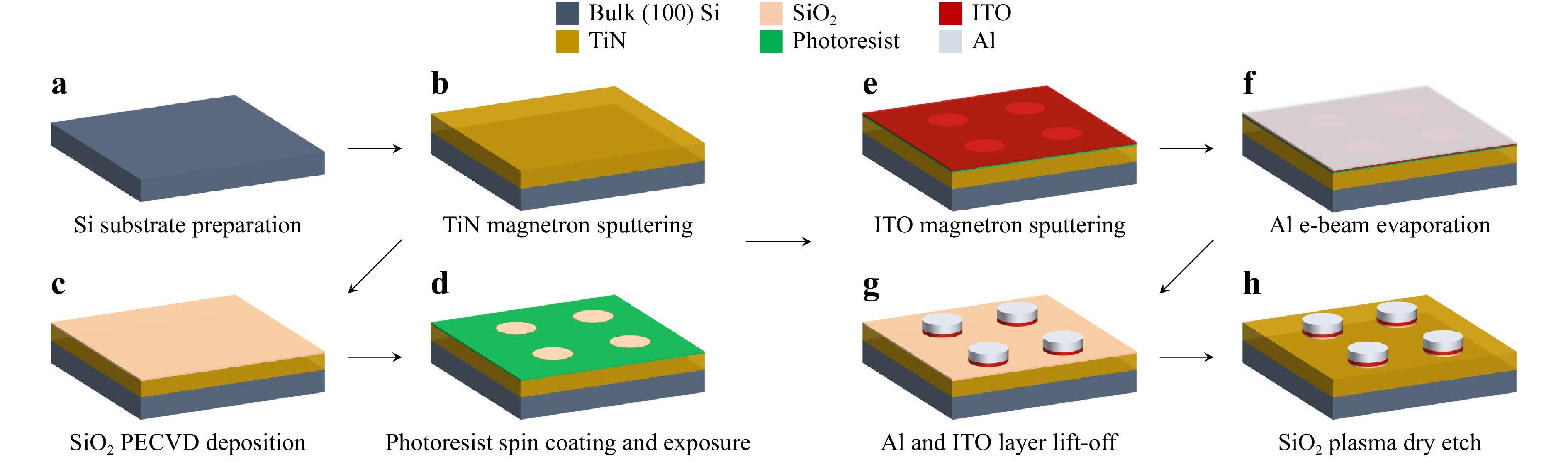
Fig. 4 TiN/Si-integrated MISM—Fabrication process: a Si wafer preparation; b magnetron sputtering of polycrystalline TiN; c SiO2 dielectric deposition; d photoresist spin coating, exposure, and development; e magnetron sputtering of ITO; f electron beam evaporation of Al; g ITO and Al lift-off; and h selective dry plasma etching of SiO2.
The poly-TiN films were deposited at a substrate temperature and bias of 700 °C and −120 V, respectively, using DC magnetron reactive sputtering of one Ti target operated at a power of 90 W in an Ar-nitrogen (N2) reactive atmosphere of 5 mTorr total pressure fed by 27 sccm of Ar and 2.2 sccm of N2 flow rates. The poly-TiN deposition rate was about 1.15 nm per min. A poly-TiN thickness of 100 nm corresponds to a deposition duration of about 75 min, high enough to ensure adequate electrical conductivity because the resistivity of thin metallic films with thicknesses lower than 100 nm is dominated by interface scattering effects36. Fig. 5a displays a grazing incidence X-ray diffraction (GIXRD) measurement performed on the grown poly-TiN layer with indexed plane peaks, confirming the polycrystalline nature of the grown thin film. Atomic force microscopy (AFM) imaging results of the grown poly-TiN film show a measured RMS roughness of approximately 1.12 nm (refer to the Supplementary Information document).

Fig. 5 TiN thin film characterization—a GIXRD survey measurement of the grown TiN layer. b IV measurements performed across two points on the grown TiN layer after dry SiO2 etching with 300 μm separation distance.
Then, as shown in Fig. 4c, an approximately 20-nm-thick SiO2 was deposited using PECVD at 330 °C, with 170 sccm SiH4/N2 and 710 sccm N2O gas flow rates and 20 W radiofrequency (RF) forward power for around 16 seconds, forming the oxide dielectric layer of the MISM. AFM imaging results of the deposited SiO2 film show a measured RMS roughness of approximately 1.36 nm (refer to the Supplementary Information document). To define the regions where Al/ITO junctions were to be formed, a bilayer lift-off process was employed whereby two PMGI SF7 and Shipley S1811 photoresist layers with total thicknesses of around 800 nm and 1 μm were successively spin-coated at 1500 and 5000 rpm, respectively, to ensure a smooth lift-off process of the ITO (~20 nm) and Al (~250 nm) relatively thick film stack. The resultant pattern is shown in Fig. 4d. An approximately 20-nm-thick ITO layer was then sputtered using RF magnetron sputtering of one ITO target (90% In2O3 and 10% SnO2 w/w%) at 150 W for 270 seconds with 50 sccm Ar and 0.50–0.80 sccm oxygen (O2) gas flows ($ {F_{{{\rm{O}}_2}}} $) at room temperature (Fig. 4e). This was followed by depositing a 250-nm-thick Al layer using an e-beam evaporator (Fig. 4f). As depicted in Fig. 4g, the deposited ITO/Al layers were lifted-off overnight in a Remover PG solution, followed by a one-minute Remover PG bath and a one-minute IPA bath, both at room temperature. The sample was then rinsed in DI water. Finally, the exposed area of the SiO2 layer was dry-etched at 20 °C using 38 sccm Ar and 12 sccm CHF3 gas flows for 35 seconds to render accessible the poly-TiN bottom electrode for electrical measurements (Fig. 4h). Fig. 5b displays current-voltage (IV) measurements performed across two points on the grown poly-TiN layer (300 μm apart) after SiO2 dry etching. These measurements show that the poly-TiN layer is conductive with a series resistance of around 26.20 Ω, confirming the complete removal of the SiO2 film after the dry plasma etch process.
-
Fig. 6 depicts a schematic illustration of the CHPW modulator fabrication process. This multi-layer-structure (i.e., a-Si/Al/SiO2/ITO) CHPW device comprises a high-index bottom dielectric layer, a low-index dielectric spacer, a metal layer, a high-index top dielectric layer, and an ITO layer that is incorporated as part of the spacer layer. For integration with Si photonics, a Soitec Unibond SOI wafer was chosen as the device platform, which has a 220-nm-thick single-crystalline Si layer serving as the bottom high-index layer. SiO2 and Al, respectively, were selected as the spacer and metal layers to ensure compatibility with CMOS processes. The top high-index layer was chosen to be a 200-nm-thick a-Si deposited at room temperature to avoid Al diffusion or oxide formation at higher deposition temperatures. Based on our previous analysis65, the width of the CHPW modulator was fixed at around 200 nm to minimize IL levels. Light is coupled in and out of the active CHPW components using 775 nm wide Si nanowires. Contact pads for the modulator were designed with 100 μm-wide pitch to match that of a commercial high-speed RF probe.

Fig. 6 a-Si/Al/SiO2/ITO CHPW modulator—Fabrication process: a SOI wafer preparation; b substrate passivation using e-beam evaporated SiO2 (5 nm); c W alignment mark deposition and lift-off; d magnetron sputtering of 10-nm-thick ITO electro-optic layer; e e-beam evaporation of 20-nm-thick SiO2; f e-beam evaporation of Al; g magnetron sputtering of 200-nm-thick a-Si; h a-Si trench formation using DRIE; i formation of Si nanowires and CHPW components by etching through the entire waveguide stack; j selective-area etching of the a-Si layer; k sputtering and subsequent lift-off of 200-nm-thick Al contact pads. Inset: Electron microscopy imaging—Bird’s-eye SEM view of a fabricated 10-μm long SiO2/ITO CHPW modulator.
To fabricate the CHPW, a bottom-up fabrication approach was implemented via the lift-off technique because of the overall higher reproducibility and device yield. The stacked layers were deposited only at the desired regions, eliminating inconsistencies from wet etching processes. The CHPW fabrication process started with SOI substrate preparation Figs. 6a–c. As depicted in Fig. 6a, the substrate was cleaned using a piranha solution ([4:1] H2SO4:H2O2 for 10 minutes), a buffered oxide etchant (BOE, for 10 seconds), and an RCA solution ([6:1:1] H2O:HCl:H2O2 for 10 minutes at 60 °C). The SOI wafers were cleaned using piranha, BOE, and RCA solutions to remove metals and organic contamination to which nanoscale waveguide operation can be sensitive. The substrate was then passivated with a sputtered 5-nm-thick SiO2 layer (at 3 mTorr working pressure, 300 W magnetron power, and 30 sccm Ar flow rate for 72 seconds at room temperature) as shown in Fig. 6b before sputtered 60-nm-thick tungsten (W) markers (at 3 mTorr working pressure, 200 W magnetron power, and 30 sccm Ar flow rate for 720 seconds at room temperature) were patterned via a lift-off process (using a patterned MMA/PMMA resist) as shown in Fig. 6c. After that, a 10-nm-thick ITO layer was sputtered to create the electro-optic layer in the modulator device region (Fig. 6d), followed by an e-beam evaporation of 20-nm-thick SiO2 layer (Fig. 6e) at room temperature. E-beam evaporated SiO2 was used instead of PECVD in the case of CHPW fabrication, given that it follows ITO deposition and ITO electro-optic properties are sensitive to high-temperature processing. This SiO2 layer would serve as the low-index spacer for the CHPW. A 10-nm-thick Al layer was then e-beam evaporated (Fig. 6f) to form the metal layer for the CHPW device and serve as an etch mask for the ITO thin film. To obtain the functional CHPW device, the areas where the input and output Si nanowires are located on the sputtered a-Si layer (Fig. 6g) were selectively patterned and etched (Fig. 6h) using deep reactive-ion etching (DRIE) to expose the regions where the input/output Si nanowires will eventually be located. The patterning was performed using an electron beam lithography tool to achieve the desired high-resolution features (100 kV accelerating voltage and beam current of 50 nA and 1 nA for the bulk and sleeve regions, respectively). The Si nanowires and CHPW components were created by etching through the entire waveguide stack (Fig. 6i), while the a-Si layer was etched afterward to reveal regions where device contacts will be made (Fig. 6j). Finally, as shown in Fig. 6k, 200-nm-thick Al pads were sputtered and lifted off to create the contact layers.
A bird’s-eye view scanning electron microscopy (SEM) image of a fabricated CHPW modulator is shown in the inset of Fig. 6. Contacts were formed by extending the Al and ITO layers away from the waveguide region via fingers that are 475 nm-wide and separated by 2 μm gaps. This was to ensure minimal disturbance to the optical mode. The anode (S) and cathodes (G), consisting of 200-nm-thick Al layers, are sputtered onto the extended Al and ITO regions. To facilitate probing, the area of the Al pads is larger than that of the existent contact region. Under an external bias, carriers are injected through the contacts, and the formation of a voltage-induced accumulation layer as the SiO2/ITO interface enables optical modulation.
Si-integrated Al/ITO/SiO2/TiN MISM
CHPW modulator
-
At the waveguide region, the Al/SiO2/ITO stack is equivalent to an MIS described by a capacitance $ C_ {\rm{MIS}} $ and a parallel (or shunt) resistance $ R_ {\rm{MIS}} $. Fig. 7 displays the capacitance-voltage ($ CV $) measurements that were performed on circular MISMs with a radius size of 100 μm. While the area-normalized capacitance values shown in Fig. 7 are reported for $ CV $ measurements performed with a small-signal frequency component of 1 MHz, the Supplementary Information document provides $ CV $ measurements performed with small-signal frequency components of 10 kHz and 100 kHz. The electrical probe station used to measure this structure is described in the materials and methods section under electronic properties. To have a properly functioning MISM device, the phase angle ($ \theta $) between the current through and voltage across the device must be around −90°C, implying that there is no significant influence of series resistance ($ R_ {\rm{s}} $) on the measured impedance ($ Z $) and hence it is entirely imaginary considering the following expression for a capacitor impedance
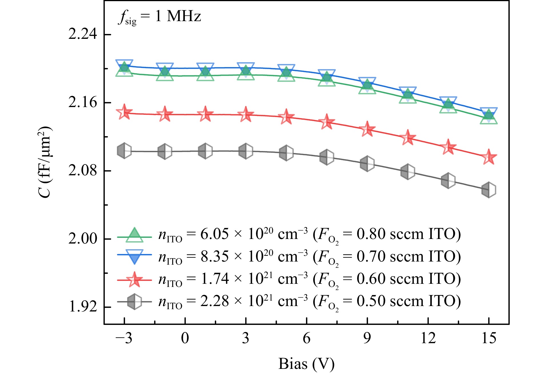
Fig. 7 MISM CV plots—Frequency response curves of fabricated SiO2/ITO MISMs with different nITO levels as functions of bias voltage.
$$ Z = R_ {\rm{s}} + \frac{1}{j\omega C} $$ (6) where $ j = \sqrt{-1} $ is the imaginary unit and C is the measured capacitance. In this case, the electrical reactance $ X_ {\rm{C}} $ is defined as $ X_ {\rm{C}} = -1/(\omega C) $ and the phase angle $ \theta_{Z} $ between the current and voltage can be calculated using
$$ \theta_{Z} = \arctan{\Bigg(\frac{X_ {\rm{C}}}{R_ {\rm{s}}}\Bigg)} $$ (7) The Supplementary Information document provides $ \theta_{Z} $ adherence curves for the poly-TiN/SiO2/ITO/Al MISM at 10 kHz, 100 kHz, and 1 MHz. By performing a small-signal analysis for the MISM capacitor structure, we calculated a negative bias resistance of 86.7 $ \mu\Omega $ with a capacitance value of 29 fF/μm2 at 20 GHz. These values, alongside the radius of the capacitor, yield an anticipated RC bandwidth of roughly 200 GHz, as obtained from calculated impedance parameters. It is worth noting that the large capacitor area relative to the thickness of the insulator and semiconductor layers yielded relatively small and large lumped series resistance and capacitance, respectively.
For an ITO layer with a $ n_ {\rm{ITO}} $ = 6.05 × 1020 cm−3 at 0.50 V and a small-signal frequency of 1 MHz, the calculated capacitance value based on simulations ranged between 1.9 and 3.07 fF/μm2 depending on the ITO and SiO2 layer thicknesses. The measured capacitance value at 0.50 V and 1 MHz small-signal frequency is 2.19 fF/μm2 as can be seen in Fig. 7. This is within the calculated capacitance range for an MISM device with around a 2.5 nm average increase in ITO and SiO2 layer thicknesses. Therefore, we must note that variations in the actual structural layer thicknesses are not the only factor that affects the measured device parameters. Fabrication process imperfections and defects must have induced parasitic effects, which led to an increase in the “effective”' dielectric and semiconductor layers thicknesses (i.e., the approximately 2.5 nm increase in ITO and SiO2 layers), further contributing to lower measured capacitance levels.
As observed in Fig. 7, with a modest variation in negative bias levels, a significant drop in normalized capacitance levels occurred at higher positive bias levels, illustrating that higher current injection levels are achieved. This is a direct result of carrier accumulation at the SiO2/ITO interface. This mechanism behind the dispersion properties of charge carriers within the semiconductive ITO layer induces the necessary capacitance modulation upon which optical modulation is directly dependent. At all small-signal frequency levels (refer to the Supplementary Information document), capacitance levels are the highest across MISM devices with $ {F_{{{\rm{O}}_2}}} $ of 0.70 sccm (sample 3, $ n_ {\rm{ITO}} = 8.35 \times 10^{20} $ cm−3) and 0.80 sccm (sample 4, $ n_ {\rm{ITO}} = 6.05 \times 10^{20} $ cm−3), demonstrating relatively more robust capacitors when the device is operating close to or well within the ENZ regime. When comparing the $ CV $ measurements performed with a small-signal frequency component of 1 MHz (Fig. 7) with those with small-signal frequency components of 10 kHz and 100 kHz (refer to the Supplementary Information document), it is worth noting that the fabricated MISM devices display relatively high-performance levels when biased with small-signal frequency levels of 100 kHz and 1 MHz. At these small-signal frequency levels, lower noise levels (at 100 kHz and 1 MHz small-signal frequencies) and higher areal capacitance levels (at 1 MHz small-signal frequency) were achieved while maintaining considerable modulation in capacitance values.
MISM devices with ITO films deposited at $ {F_{{{\rm{O}}_2}}} $ = 0.70 and sccm have higher oxygen contents and therefore are less conductive. The ITO optical attributes described in Figure S1 of the Supplementary Information document illustrate how the dielectric constant, and hence the refractive index, varies with carrier concentration. As the carrier concentration increased through doping, there were points where the properties of ITO transitioned from those of a conductor to a semiconductor and then to an insulator66. Therefore, the $ CV $ measurements done on these ITO films deposited at different ${F_{{{\rm{O}}_2}}} $ levels are expected to reflect a trend of increasing refractive index for higher $ {F_{{{\rm{O}}_2}}} $67.
In Fig. 7, we can observe that at a negative bias around −1 V, there are dips in capacitance levels, where depletion occurs and $ {\rm {Re}}\{n\} $ drops, and hence the ITO electrical properties at the interface shift towards those of a conductive dielectric and thus start to exhibit smaller capacitance values. For small positive bias values (partial forward bias), we conjecture that the observed $ CV $ curves follow the $ {\rm{Re}}\{n\}{\text -}V $ curve exhibited in Fig. 2b. As the bias increases, accumulation effects occur, contributing to higher capacitance levels. At negative bias levels, the shape of the $ CV $ curves resembles an inversion-region operation, and hence the capacitance levels start to increase again. We also observe what resembles a roll-out at higher positive bias levels, which is possible cause by other competing effects. For instance, enhanced optical confinement is possible, implying an enhanced overlap with the electric field, which lowers capacitance levels. This phenomenon can be explained by the effects of plasma and the correlations between optical parameters and carrier density68. $ {\rm{Re}}\{\varepsilon\} $ is related to the energy stored within a medium and is affected by capacitance and $ {\rm{Im}}\{\varepsilon\} $ is associated with the loss or gain of energy within a medium. Capacitors with ITO films deposited at higher ${F_{{{\rm{O}}_2}}}$ are more resistive and therefore exhibit higher $ {\rm{Re}}\{\varepsilon\} $, which intuitively explains the greater capacitance levels displayed by ITO films deposited with ${F_{{{\rm{O}}_2}}}$ = 0.70 and 0.80 sccm. Finally, we note that as the operating frequency of the MISM devices gets higher, the $ CV $ curve gets smoother. This is probably caused by the noises being relatively lower in the driving frequency source. While for the 10 kHz operating frequency case, there are more noticeable slight dips in the capacitance levels around −1 V compared to higher operation frequencies. This may be caused by the higher modulation speed of carriers at the SiO2/ITO interface.
-
Fig. 8a displays the forward-biased $ IV $ response of the CHPW, manifesting an irreversible oxide breakdown around 35 V. This corresponds to a SiO2 dielectric strength of 17.5 MV/cm. The tunneling current up until 25 V bias was less than 2 nA, which indicates excellent capacitive coupling characteristics, and thus the shunt path bypassing the capacitor can be neglected (i.e., $ R_ {\rm{MIS}} \rightarrow \infty $). Moreover, the device’s capacitance was determined at an AC frequency and voltage of 1 MHz and 10 mV$ _ {\rm{rms}} $, respectively. Because of the compact device footprint nature and instrument resolution limitation, the high-frequency branch of the MIS $ CV $ curve could not be observed. $ C_ {\rm{MIS}} $ for the 5- and 10-μm long devices were measured to be about 3 fF and 5 fF, respectively, at a bias of 25 V. Fig. 8b displays the photocurrent characteristics. At 10 V, the MIS photodiode exhibited a photocurrent-to-dark ratio of 5.77.
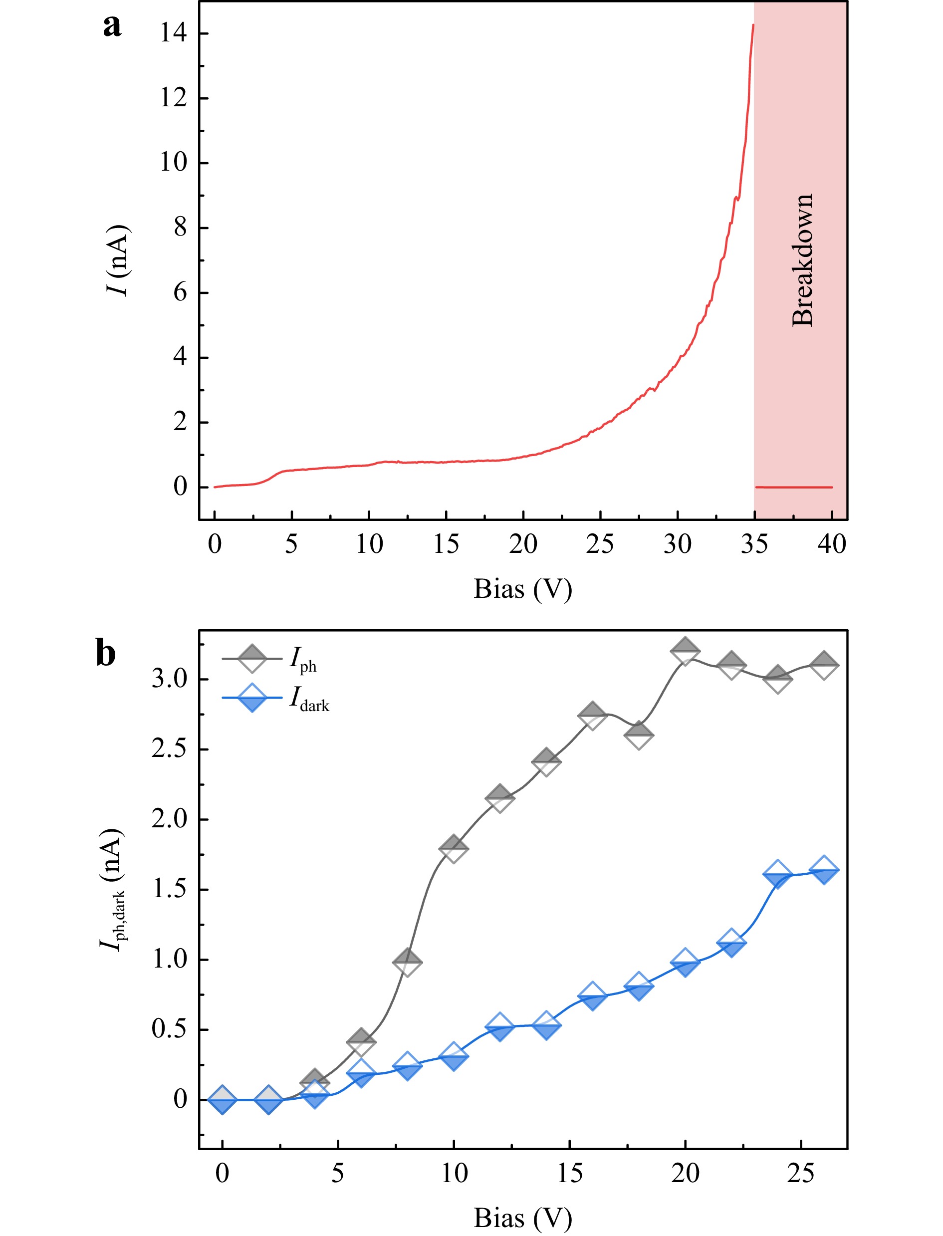
Fig. 8 CHPW IV response—a Measured IV characteristics demonstrating a breakdown voltage around 35 V. b Measured dark- and photocurrent characteristics.
Several contact resistance terms are considered when describing the modulator’s electrical characteristics. The probe contact resistance is negligible as the coaxial high-frequency infinity waveguide probe used for device characterization has a typical contact resistance below 0.1 Ω to Al pads. The series resistance from the sputtered Al contact (around 5 Ω) is small relative to that of the other sputtered thin films, as their resistivities were measured to be between 8 × 10⁻⁷ Ω·cm and 2.9 × 10⁻⁴ Ω·cm. Therefore, the modulator resistance is dominated by the series resistance $ R_ {\rm{s}} $ of ITO and the contact resistance $ R_ {\rm{c}} $ between Al and ITO. Based on the dimensions of the fingers and modulators, $ R_ {\rm{s}} $ was determined to be 911.2 $ \Omega $ and 896.6 Ω for modulator lengths of 5 and 10 μm, respectively.
The $ R_ {\rm{c}} $ for the CHPW modulator was determined via circular transmission line measurement (CTLM). CTLM is preferred over standard transmission line measurement for devices with micron-scale areas as current crowding can be avoided, and electrical isolation is automatically established69. As shown in the inset in Fig. 9, the CTLM test structure consisted of a conducting circular inner region of radius L, an air gap of width d, and a conducting outer part70, 71. Specifically, the total resistance $ R_ {\rm{T}} $ between the internal and external contacts can be expressed as

Fig. 9 Contact resistance characterization—a A plot summarizing CTLM results for the Al (250 nm)/ITO (10 nm) contacts with L = 75 μm. b IV curves for a CTLM structure with d = 10 μm and L = 75 μm.
$$ R_ {\rm{T}} = \frac{R_ {\rm{sh}}}{2\pi L}(d + 2L_ {\rm{T}})\mathbb{C}, $$ (8) where $ R_ {\rm{sh}} $ is the sheet resistance, $ \mathbb{C} $ is a correction factor, and $ L_ {\rm{T}} $ is the transfer length describing the average distance traveled by carriers within the semiconductor region. These two parameters were calculated as $ \mathbb{C}=L/d\ln(1+d/L) $ and $ L_ {\rm{T}} = \sqrt{\rho_ {\rm{c}}/R_ {\rm{sh}}} $, where $ \rho_ {\rm{c}} = R_ {\rm{c}}(\pi L^{2}_ {\rm{T}}) $ is the specific contact resistivity that takes into account all interfacial effects and effects from regions close to the interface71. CTLM results from the ITO/Al interface are depicted in Fig. 9. The conducting regions consisted of 250-nm-thick Al on 10-nm-thick ITO on SOI. Because ITO is a highly degenerate semiconductor, the barrier height and the width of the depletion region at the ITO/metal interface are small. Therefore, ITO forms an ohmic contact with metals, allowing for smooth carrier injection. Using the measured $ R_ {\rm{sh}} $ of 290 $ \Omega/\square $, the $ \rho_ {\rm{c}} $ of the CTLM structures is extracted to be 7.2 × 10⁻³ Ω·cm2. This is significantly lower than the 3 × 10⁻¹ Ω·cm2 previously reported for ITO/Al contacts with similar $ R_ {\rm{sh}} $ values72, but higher than 10−6Ω·cm2 as estimated by the standard metal/semiconductor contact theory 73. Such deviation from theoretical value is common for ITO devices, as the interaction between oxygen and metal has been observed to alter ITO’s carrier density at the interface and thus leads to an increase in $ \rho_ {\rm{c}} $. With contact area of 82.72 μm2, the $ R_ {\rm{c}} $ for the fabricated CHPW modulators was measured to be 8.7 kΩ.
-
Lower carrier concentrations lead to lower optical losses, which result in better modulator’s IL but at the expense of lower conductivity, implying lower $ RC $ time constants. Therefore, we require the carrier mobility to be as high as possible to increase the conductivity without increasing the carrier concentration, leading to lower insertion and optical losses. The sheet resistivity of ITO is strongly correlated with the O2 and Sn contents. The density of free electrons in ITO is directly influenced by O2 vacancies, with an inverse proportionality to the O2 content. On the other hand, the electron mobility in ITO is heavily influenced by the O2 content, as higher O2 contents enhance the crystallization of ITO thin films74.
-
Unbiased-state CHPW modulator characterization has been performed using the cut-back method. As observed in Fig. 10, the IL and CE at $ \lambda = 1550 $ nm were extracted to be around 0.128 dB/μm and 52.50%, respectively. The loss value is higher than the simulated value of 0.03 dB/μm (simulations are not shown here). The higher experimental IL level is attributed to the additional free carrier absorption caused by elevated ITO carrier density and scattering losses from the contact region. Effects from deposited layer roughnesses and various intrinsic defects, such as surface states and oxygen vacancies, could have played an additional role in this higher measured IL level75-77. Nonetheless, IL and CE values exhibit low variations between $ \lambda = 1520 $ nm and 1600 nm, indicating a potential broadband modulator operation.
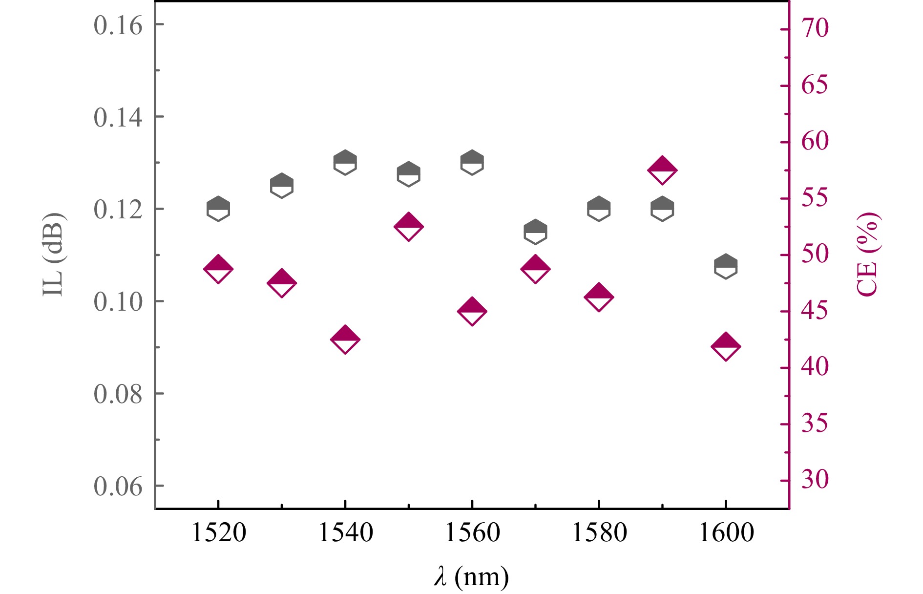
Fig. 10 CHPW unbiased response—Extracted IL and CE values of the CHPW modulator as functions of wavelength.
-
Fig. 11a plots the transmission of 10-μm-long CHPW modulators under forward bias. The maximum voltage was kept below 26 V to avoid oxide breakdown, and the results have been normalized to optical transmission at zero bias. We note that the observed optical transmission level decreases marginally to a small extent as the voltage is increased up to 20 V. After the applied voltage exceeds 20 V, a dramatic increase in optical absorption takes place, and transmission is reduced to −10 dB at 25 V, which corresponds to strong ER of approximately 1 dB/μm, one of the highest measured to-date to our knowledge6. The reason for resorting to applying a high voltage level of 20 V is that a 20-nm-thick SiO2 (rather than a high-κ dielectric material) layer was incorporated in the MOS region of the modulator for simplicity of design, hence the facile integration of SiO2/ITO. In other words, our CHPW design necessitates applying a relatively high electric field, given the relatively low dielectric constant of SiO2, which serves as a reference to other field-confining materials. The voltage can be reduced to improve the modulation efficiency by incorporating a high-κ dielectric material instead, such as hafnium oxide (HfO2).
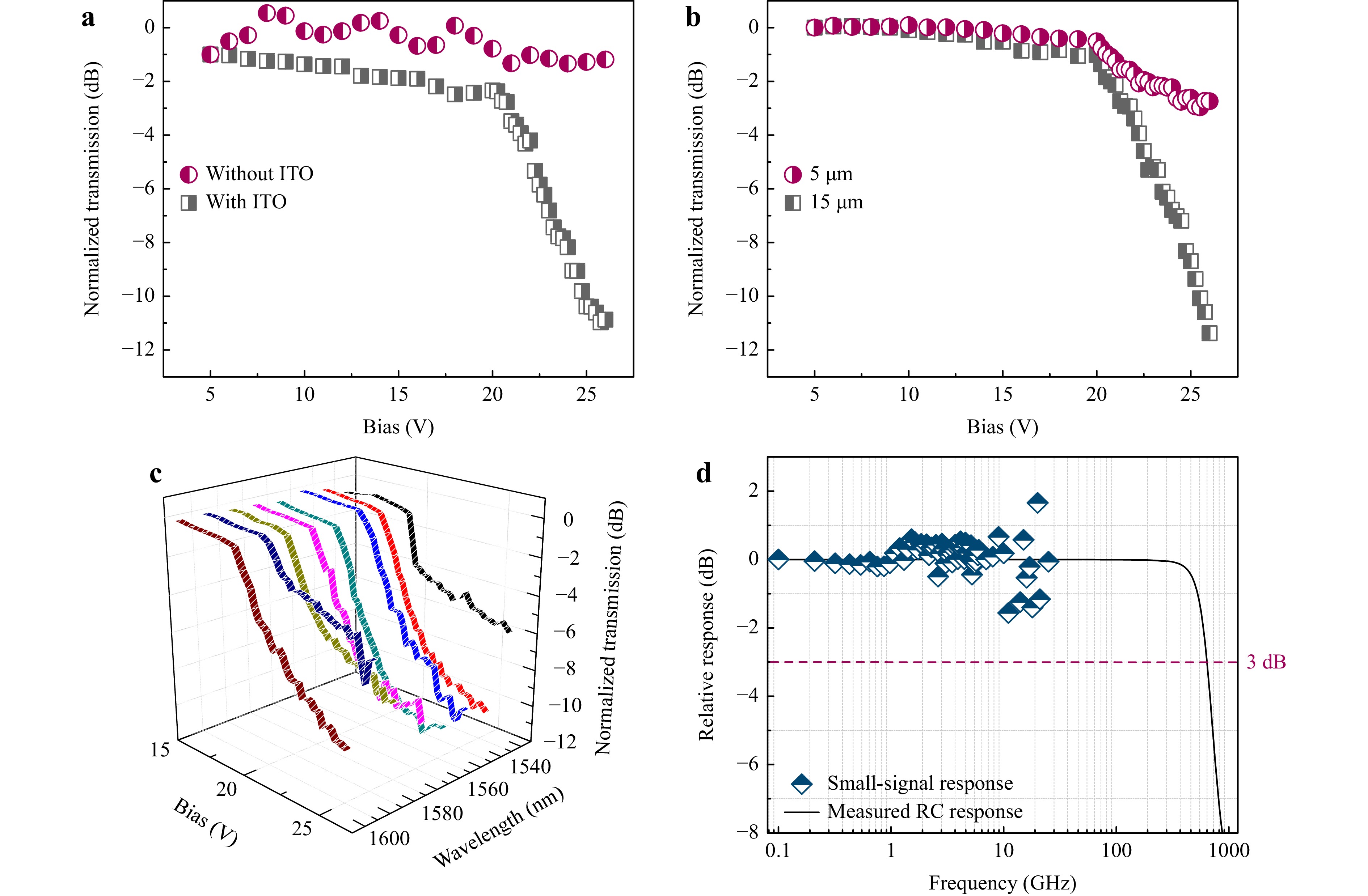
Fig. 11 CHPW DC/AC response—a Normalized transmission curves of a 10-μm-long SiO2/ITO-based CHPW modulator as functions of bias voltage. The behavior of the modulator without an ITO layer is also displayed. b Normalized transmission of 5- and 15-μm-long SiO2/ITO-based CHPW modulators as functions of bias voltage. c Normalized transmission curves of a 10-μm-long SiO2/ITO-based CHPW modulator as functions of bias voltage and wavelength. d Optoelectronic bandwidth measurements of the SiO2/ITO-based CHPW modulator.
The behavior of the same modulator without an ITO layer is also provided for comparison. As no modulation can be observed under both scenarios, the measured modulation response can be attributed to field-induced carrier accumulation rather than drift in the set-up, optothermal effects at high bias voltages, or optoelectronic events in materials other than ITO. Moreover, modulation depth varies with device length, and the normalized transmission for a 15-μm-long modulator can reach −12 dB at 26 V as can be seen in Fig. 11c, where the broadband response of the CHPW modulator is shown. It was verified by measuring the optical transmission as a function of voltage at different wavelengths (from $ \lambda = 1.53 $–1.6 μm), as shown in the figure. Beyond $ \lambda = 1550 $ nm, the modulation depth starts to decrease as the permittivity of ITO moves away from the ENZ regime. However, an ER of about 1 dB/μm was maintained between $ \lambda = 1.53 $ μm and 1.56 μm.
-
Fig. 11d depicts the 10-μm-long modulator’s frequency response. One can observe that the frequency response is flat up to about 26 GHz, and the calculated 3-dB cutoff frequency (i.e., anticipated $ RC $ bandwidth), given a parasitic capacitance of 5 fF, is approximately 636 GHz for 50 Ω load resistance. The frequency response measurement, including the substrate characteristics and effects from the RF probe, was normalized to the response peak point. Using small-signal analysis, we calculated the junction current at 0 V. We extracted the resistance from the real part of the resulting impedance for operating frequencies up to 636 GHz at the CHPW’s SiO2/ITO heterojunction. At static and up to 26 GHz, the resistance was found to be around 75.6 Ω at 0 V, while the junction capacitance was calculated numerically using the finite difference method (i.e., $ dv/dq $ with infinitesimal voltage steps) and was estimated to be around 0.21 fF/μm (normalized to the propagation distance). For operating frequencies from 26 to above 636 GHz (up to 700 GHz), the heterojunction resistance and capacitance levels dropped dismally to approximately 73.6 Ω and 0.18 fF/μm, respectively.
The modulation speed of a CHPW is determined by two factors: (1) the time the accumulation layer inside the semiconductor takes to form, and (2) the delay time arising from parasitic $ RC $ effects. Electron accumulation is a relatively fast process dictated by majority carrier dynamics. The formation time can be estimated using $ \tau = t/v_ {\rm{drift}} $, where, in our case, $ t = t_ {\rm{ITO}} = 10 $ nm and $ v_ {\rm{drift}} $ are the ITO film thickness and the drift velocity of carriers in ITO, respectively. Here, $ v_ {\rm{drift}} $ can be estimated using $ v_ {\rm{drift}} = \mu E $, where μ is the carrier mobility in ITO and $ E $ is the applied electric field. The latter is proportional to the magnitude of applied gate voltage divided by the dielectric film thickness ($ t_ {\rm{SiO _{2}}} = 20 $ nm). Using $ \mu = 33 $ cm2/(V·s) as obtained from Hall measurements, the resulting modulation speed exceeds 300 THz. Similarly, the electron scattering rate of ITO is around 28.65 THz as derived from the collision frequency ($ \gamma = 1.8 \times 10^{14} $ rad/s); hence, the modulator speed is also not limited by the transient response of the accumulation layer when the gate is turned off78. Thus, similar to other MIS-based modulators, our CHPW modulator’s speed is dictated by the $ RC $ time constant79. While the $ RC $ response of the 10-μm-long CHPW modulator has an anticipated 3-dB cutoff frequency above 600 GHz, the bandwidth of the testing instrument used to characterize the modulator is limited to 26 GHz. Because the response of light to the plasma dispersion effect is significantly faster than the $ RC $ limit, delays from strong local field decays can be disregarded, and, as a result, the theoretical electrical modulation speed of 636 GHz is directly relevant to the optical domain.
-
The performance of the 10-μm-long CHPW modulator was characterized over broad wavelength and temperature ranges. The evolution in the modulator’s ER level at elevated stage temperatures (T = 35–100 °C) relative to the modulator’s response at room temperature (ΔERRT, calculated as an absolute numerical difference) is shown Fig. 12 as a function of voltage. Because of power output limitations in the thermoelectric cooler (TEC) source meter, the Peltier heat pump requires a voltage-limited mode of operation, and, therefore, the stage temperature exhibited a ±0.2 °C fluctuation. Regardless of the noise caused by temperature fluctuations, the modulator’s ER performance did not degrade; instead, it increased with increasing stage temperature. For instance, an approximately 0.74 dB increase in ER was detected at 50 °C and 100 °C at 25 V.
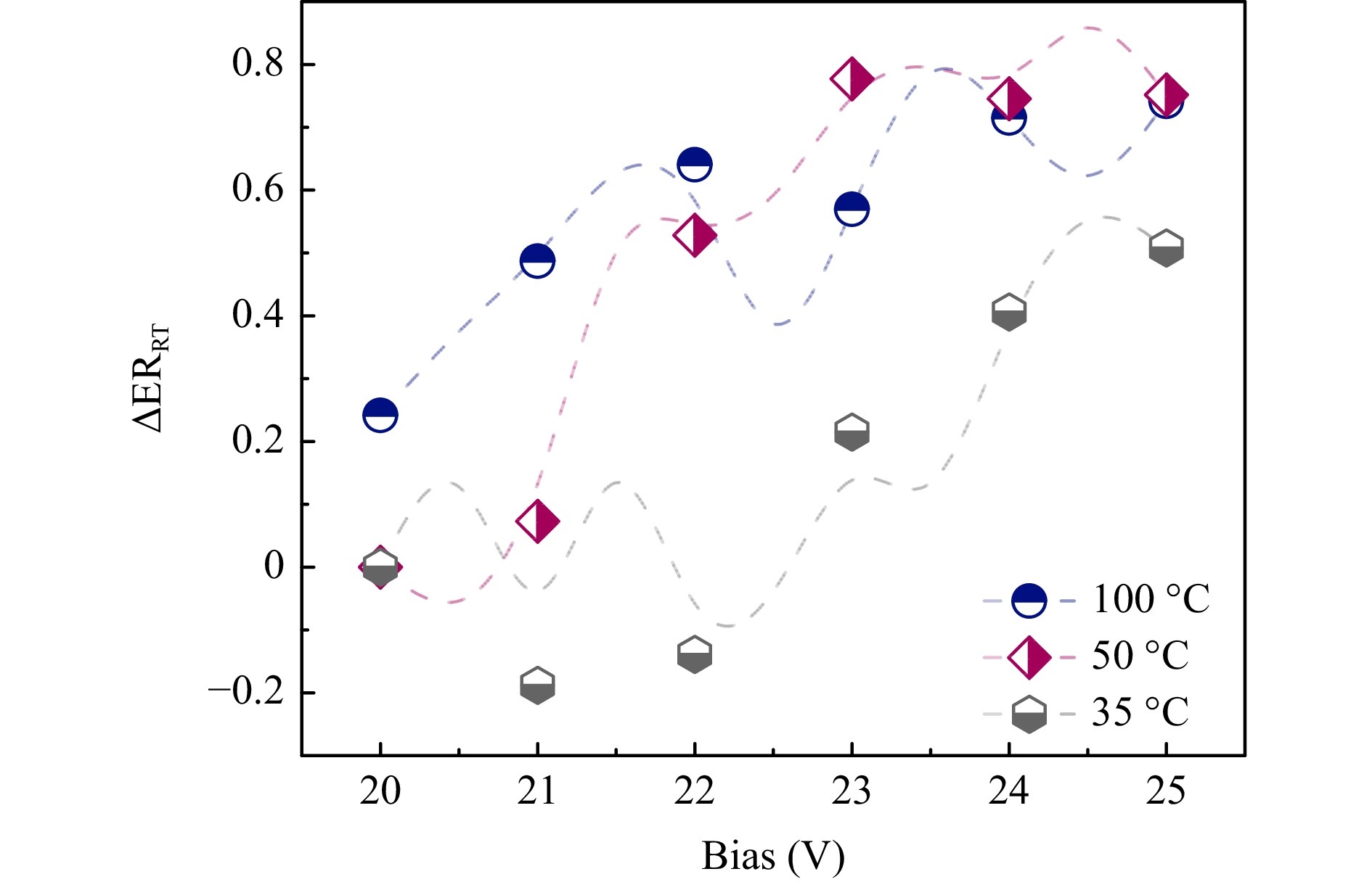
Fig. 12 CHPW ER analysis—Evolution in the modulator’s ΔERRT (its ER level at various elevated stage temperatures relative to its response at room temperature) as a function of bias voltage.
MISM $ CV $ characterization
CHPW electrical characterization
CHPW optical modulator characterization
CHPW unbiased response
CHPW DC response
CHPW AC response
CHPW ER analysis
-
We have successfully demonstrated the facile growth, integration, and characterization of Al/ITO/SiO2 MISM heterojunctions on a poly-TiN/Si platform, facilitating the design and fabrication of practical CHPW devices. The research focus on oxide materials for plasmon-electronics has significantly surged, given its potential to achieve tunable material characteristics. However, achieving optimal device performance requires extended optimization of material quality, device design, and process technology. Herein, we focused on developing insulator–semiconductor device topologies by integrating an electro-optic SiO2/ITO interface in MIS devices housed on bulk Si and SOI platforms. The advantage of this integration scheme is rooted in the use of CMOS-compatible materials, along with breaking the loss-confinement barrier in plasmon-electronic devices by tuning the waveguide architectural characteristics and hence achieving control over supermode attributes. XRD, $ IV $, $ CV $, and parameter analyzer measurements were used to characterize the grown materials and fabricated devices. The fabricated CHPW modulator shows ER and IL levels of around 1 dB/μm and 0.128 dB/μm, respectively, for a 10-μm-long waveguide length. While our initial device performance seems promising, challenges still exist, and these are the development of the ability to produce large-area optoelectronic devices using current material synthesis and device fabrication methodologies. Table 2 summarizes our CHPW modulator performance and provides a performance comparison with select modulator configurations as reported in the literature.
Modulator device structure Footprint (μm2) Speed (GHz) Operation wavelength (nm) Driving voltage (V) ER (dB) Ref. MIS–Schottky CHPW 10 × 0.2 >600 1550 25 10.63 This work MISM capacitor 3 × 10⁴ >200 1550 15 – This work Plasmonic Si Mach–Zehnder 10 × 1 >70 1550 3 6 Haffner et al. 80 Graphene-based Si waveguide 50 × 10 5.9 1550 2.5 5.2 Hu et al. 81 Electro-optic graphene 1.5 × 30 >150 1570 10 28 Phare et al. 82 Table 2. Summary of fabricated CHPW modulator performance parameters, along with performance comparison with select modulator configurations.
-
The ITO and a-Si thin films were deposited using an AJA International twin chamber RF magnetron sputtering system (ATC Orion Series). The ITO and a-Si deposition processes were performed at room temperature with a working pressure of 3 mTorr. The magnetron power was fixed at 150 W and 300 W for the ITO and a-Si targets, respectively. During the a-Si thin film sputtering, an Ar gas flow of 30 sccm was flown for 200 seconds, yielding a 200-nm-thick thin film.
The ITO target was 3 inches in diameter which is 90% In2O3 by weight. Multiple ITO thin films were deposited with an Ar gas flow rate set at 50 sccm at room temperature. The O2 flow rate was varied as follows: ${F_{{{\rm{O}}_2}}}$ = 0.50 (sample 1, $ n_ {\rm{ITO}} = 2.28 \times 10^{21} $ cm−3), ${F_{{{\rm{O}}_2}}}$ = 0.60 sccm (sample 2, $ n_ {\rm{ITO}} = 1.74 \times 10^{21} $ cm−3), ${F_{{{\rm{O}}_2}}}$ = 0.70 sccm (sample 3, $ n_ {\rm{ITO}} = 8.35 \times 10^{20} $ cm−3), and ${F_{{{\rm{O}}_2}}}$ = 0.80 sccm (sample 4, $ n_ {\rm{ITO}} = 6.05 \times 10^{20} $ cm−3). This was done to demonstrate the effects of varying the gas flow on the conductivity of the deposited films. To optimize the material deposition process for optimal conductivity, ITO thin films were deposited on fused silica substrates, then characterized electrically using Hall effect measurements to determine the carrier concentration n and optically using ellipsometry to determine their thicknesses. The growth conditions of sample 4 were ultimately chosen to deposit the ITO thin films used in the MISM and CHPW device fabrication processes, given that it resulted in an optimal modulator’s IL (detailed optimization results are not shown here for conciseness).
-
Crystal structure properties of the deposited TiN thin film were examined by a Panalytical MRD glancing incidence XRD (GIXRD) system using copper (Cu) $ K\alpha $ radiation in line mode. On the incident side, the system is equipped with a mirror and slits, whereas on the receiving side, the system is equipped with a parallel plate collimator.
-
The electrical properties of TiN and ITO, namely the charge carrier density and mobility, as well as the electrical resistivity and Hall coefficient ($ R_ {\rm{H}} $), were determined at room temperature in a van der Pauw configuration of electrodes using a Nanometrics HL5500 Hall measurement system with a constant magnetic flux density of 0.504 T.
MISM: The MISM $ CV $-$ IV $ measurements were performed in an electrical probe station equipped with an Everbeing International Corp. probe station C-8 with a shielding box and vibration isolation. The measurements were collected and analyzed using a Keithley 4200A-SCS Parameter Analyzer with a supply voltage range of 100–240 V$ _ {\rm{rms}} $ at 50 or 60 Hz and 1000 VA current rating.
CHPW: The $ IV $ response of a 10-μm-long Al/SiO2/ITO CHPW structure was measured using an HP 4155A semiconductor parameter analyzer. The device capacitance was determined using an HP 4280 $ CV $ meter. Moreover, the optoelectronic bandwidth of the CHPW modulators up to 6 GHz was measured using an RF signal that was generated by a National Instrument (NI) PXIe-5673E RF vector signal generator (VSG) with 6 dBm peak-to-peak amplitude and a rectangular shape. A bias-tee set before the input of the RF probe was used to combine the RF signal with DC offset from a Keithley 2604B source meter. The resulting amplitude-modulated optical signal was captured via a New Focus 1454 18.5 ps Vis-IR photodetector and amplified with an AMF 00101000-55 amplifier before being fed into an NI PXIe-5663E vector signal analyzer (VSA) for analysis. The electrical bandwidth of the CHPW photodetector was quantified using the NI PXIe-5673E VSG and PXIe-5663E VSA. On the input side, the VSG stimulus was amplified and drove a Fujitsu LiNbO3 Mach–Zehnder modulator, generating intensity-modulated optical signals up to 6 GHz. On the output side, the photocurrent was collected with a coaxial high-frequency Infinity waveguide probe and amplified before feeding into the NI PXIe-5663E VSA. Measurements with the laser beam turned off were also performed to subtract coherent electrical input-output crosstalk. For measurement between 6 and 26 GHz, the same setup with Keysight M9375A PXIe vector network analyzer (26.5 GHz, 6-port) and AMF-4F060180 amplifier were used.
-
The surface morphology of deposited crystals was assessed using Bruker Dimension FastScan atomic force microscope operating in tapping mode. The images were recorded from 4 μm × 4 μm areas with a resolution of 1024 × 1024 pixels at a scan rate of 1 Hz, using a commercial ScanAsyst-Air pyramidal silicon nitride probe.
Thin film deposition and material characterization
X-ray diffraction crystallography
Electronic properties
Atomic force microscopy
-
This work was supported by the Natural Sciences and Engineering Research Council of Canada. The authors acknowledge access to the Quantum-Nano Fabrication and Characterization Facility (QNFCF) and the Waterloo Advanced Technology Laboratory (WATLab) at the University of Waterloo. The authors also acknowledge access to Prof. Nazir Kherani's laboratory at the University of Toronto to conduct Hall effect measurements. N. A. acknowledges the support of the Ibn Rushd Postdoctoral Fellowship Program, administered by the King Abdullah University of Science and Technology (KAUST).

 DownLoad: