


-
Integrated optical signal distributing, processing and sensing networks that rely on complex optoelectronic and plasmonic architecture requires a high degree of miniaturization of basic optical elements, i.e. waveguides1–3, splitters4–6, gratings7–9 and optical switches10,11. In an integrated system, a high field confinement is preferred toward the achievement of functionality at the integrated level. This is given for the case of subwavelength lateral dimension that enables single mode operation. To realize this type of structures, fabrication approaches allowing for high-resolution manufacturing are demanded. On the other hand, curved elements such as bending optical features12 and especially ring resonators13,14, which are popularly employed in integrated networks and exploit interference effects, require even higher fabrication resolution as well as low sidewall roughness. Therefore, fabrication techniques with a precise control of absolute structure dimensions are imperative. So far, several technologies have been developed for the required subwavelength high-resolution manufacturing15, i.e. direct laser writing16–18, multi-photon lithography19–22, electron beam lithography23,24, ion beam lithography25,26 and domino lithography27,28. However, the fabrication systems based on these techniques are costly and complex. In addition, the involved fabrication processes are usually time-consuming. Nanoimprint lithography is an emerging replication technique for high-resolution and efficient manufacturing29–31. However, it requires high-quality master stamps, which are usually produced using the aforementioned costly and relatively slow electron beam lithography. In contrast, optical contact lithography32,33 and projection photolithography34,35 using high-resolution masks from commercial photoplotters are also being developed for micro- and nanostructuring. While possessing the advantages of lower cost and improved efficiency, they can only achieve resolution down to a few micrometers. The realization of subwavelength resolution still remains challenging.
In this work, we demonstrate a cost-efficient and user-friendly fabrication approach, called UV-LED-based microscope projection photolithography (MPP), for rapid high-resolution manufacturing of optical elements within seconds. This approach implements structuring by transferring structure patterns on a photomask to a photoresist-coated substrate under UV illumination. The fabrication system was established using standard optical and optomechanical elements. Instead of a mercury lamp or a laser, an extremely low-cost UV-LED with a wavelength of 365 nm was employed as the light source for this system. To obtain the structure-patterned chromium mask required in MPP, preceding process steps including the structure design, printing on a transparent foil, as well as a subsequent lithography for the preparation of a chromium photomask were developed. A lithography setup was established as well for the preparation of photomasks. With this setup, structure patterns printed on a transparent foil can be transferred to a chromium photomask, by combining a subsequent wet ecthing process.
On the basis of this approach and the developed systems, subwavelength resolution was achieved through optimizations in each processing step. First, printing approaches including inkjet printing and laser plotter printing were employed to print the designed structure patterns onto a transparent foil with their printing quality and resolution compared. For the chromium photomask preparation, two different lenses were also respectively implemented into the setup for transfer of structure patterns from the transparent foil to the chromium and the photoresist-coated substrate. Their performance in structuring accuracy (referring to the printing error of the fabricated dimension to the designed value) due to field-dependent aberrations was compared and analyzed. On that basis, final structuring using UV-LED-based MPP was demonstrated. To minimize the imaging aberrations, tube lenses were employed in the established setup to create an infinity corrected optical system with the combination of a microscope objective. By use of a 100x objective with a numerical aperture (NA) of 1.4 (Carl Zeiss), a minimum feature size down to approximately 85 nm was successfully achieved. Furthermore, an economic 100x microscope objective with a NA of 1.25 (Müller Optronics) was employed for the realization of structures using the same chromium photomask to verify the stability and functionality of the developed approach. With this economic objective, a minimum feature size of approximately 100 nm was realized. In addition, gratings with an area size of 100 µm × 100 µm and a pitch of 1 µm were fabricated using both objectives and another 100x microscope objective (NA 0.95, Carl Zeiss), respectively, and the structure formation, measured gap sizes and linewidths were compared. The grating produced with the economic objective exhibits a little out-of-focus area at the grating corner and a larger gap size than the other two higher-cost objectives, which probably results from the remaining field curvature. Nevertheless, the results show that the proposed fabrication approach is able to realize high-resolution structuring with sub-100 nm feature size, which is below the diffraction limit.
-
Three processing steps are mainly included towards the proposed UV-LED-based MPP. First, desired structure patterns were designed using CorelDraw and printed on a transparent foil. Afterwards, the printed transparent foil was placed into a home-built setup to transfer the structure patterns onto a fresh photoresists-coated chromium mask. A structure-patterned photomask was obtained with a subsequent wet etching, which was then placed into the developed MPP setup for the micro- and nanostructuring. This process chain was developed to ensure high flexibility for the pattern structuring and minimize the time expense for location transfer for different processing steps. Regarding fabrication resolution, it is restricted by the diffraction limit of the optical manufacturing system. On the other hand, it is also determined by the printing quality and accuracy of patterns on the transparent foil and the chromium photomask. Here, we report the investigation of the printed pattern accuracy and quality on the transparent foil by different approaches and the performance of two different optical lenses employed in the optical system for the preparation of the chromium photomask.
-
Two approaches, inkjet printing (Canon, iP4850) and laser plotter printing (Bungard Elektronik, Filmstar Plus), were employed to create the designed patterns onto a transparent foil, which is used subsequently for the preparation of chromium photomask with a 10 to 1 demagnification projection setup (see the next subsection). It has to be noted that the transparent foil used is a standard copy transparency in the case of inkjet printing and a commercial transparent film (Bungard Elektronik) in the case of laser plotter printing. Both materials are basically transparent for the 407 nm illumination. To compare the printing accuracy and quality, multiple lines with different widths in the range from 10 µm to 1000 µm were designed using CorelDraw. They were then printed using both approaches, with microscope images of some line patterns shown in Fig. 1. Fig. 1a, b display optical microscope images of lines with different designed widths printed on a transparent foil using an inkjet printer with a theoretical printing resolution of 600 dpi (equal to approximately 32.44 µm) and a laser plotter with a high printing resolution of 16,256 dpi (equal to approximately 1.56 µm), respectively. Measured linewidths of all lines are plotted in Fig. 1c.

Fig. 1 Comparison of printing results using an inkjet printer and a laser plotter. Microscope images of printed lines with different designed widths (Wdesign) by the use of inkjet printer (a) and laser plotter (b), respectively. a Lines with different designed linewidths printed by an inkjet printer with a theoretical printing resolution of 600 dpi. The minimum linewidth that can be achieved by this printing approach is approx. 75 µm. b Lines with different designed linewidths printed by a laser plotter with a printing resolution of 16,256 dpi. Much better printing quality and higher printing resolution were achieved with this printing approach. c Comparison of printed linewidths using inkjet printing and laser plotter printing.
For the case of inkjet printing, it can be seen that the measured structural dimensions remain similar for lines with designed widths below 100 µm and agree with the designed dimensions starting from 200 µm. For lines with designed widths up to 100 µm, printed linewidths of approx. 75 µm were measured. This is the minimum linewidth that can be achieved by this approach, which is different from the aforementioned theoretical printing resolution. The reason is that the overall achievable resolution of the inkjet printing also depends on the positioning accuracy of the ink nozzle and the pointing-instability of the flying droplets. In the subsequent photolithography processes, the printed dimension will be demagnified. For example, a line structure with a printed dimension of 200 µm yields to a minimum feature size of 2 µm and 200 nm, respectively, with a demagnification of 100x and 1000x. The sawtooth appearing on the edge of the line results from the use of ink droplets in the printing process. This edge roughness will also be transferred to the chromium mask and subsequently to the final lithographic structures. To ensure better functionalities of optical structures, this effect should be minimized.
In the case of the laser plotter, structure patterns were printed into a photosensitive silver layer, which is embedded into a transparent polymer foil. It can be clearly seen from Fig. 1b that this approach enables a smoother edge of the printed patterns. A difference of linewidths compared to the inkjet-printed ones is obvious. The result shown in Fig. 1c exhibits a good agreement between structural and designed dimensions. A minimum dimension down to 10 µm can be achieved. This yields a theoretical minimum feature size of 100 nm and 10 nm, respectively, with the demagnification of 100x and 1000x. The minimum feature size that can be achieved in reality is also limited by the optical diffraction limit. Compared to the results obtained via inkjet printing, laser plotter printing is advantageous in both printing resolution and quality. It exhibits the potential of achieving sub-100 nm feature size below the diffraction limit.
-
To transfer the structure patterns onto a photomask for the subsequent MPP, an optical setup was established to enable the preparation of chromium photomasks with desired patterns. A sketch of this setup is shown in Fig. 2a. An UV-LED at 407 nm with high-power output of 4.9 W was employed as the light source. The printed transparent foil was placed under a Fresnel lens. Structure patterns can be transferred onto the photoresist-coated chromium mask layer using a focusing lens or lens system. The chromium mask was prepared by depositing a chromium layer onto an 1 inch glass substrate with a thickness of 1 mm using magnetron sputtering. The chromium layer thickness is approximately 100 nm. A photoresist was spin-coated onto the top of the chromium layer used for structuring of the chromium mask. Here, resists, i.e. S1805 (Shipley), AZ1505 (MicroChemicals) or ma-P 1205 (micro resist technology) can be employed. The spin-coating parameters were taken from the processing guidelines of the corresponding photoresist. This photoresist-coated chromium mask was placed into the focal plane of the focusing lens. The pattern on the transparent foil was transferred onto the photoresist layer after UV illumination of approx. 60 s. With a subsequent development and wet etching process, the patterns can be transferred into the chromium layer. This structure-patterned chromium mask can then be used for the MPP process.
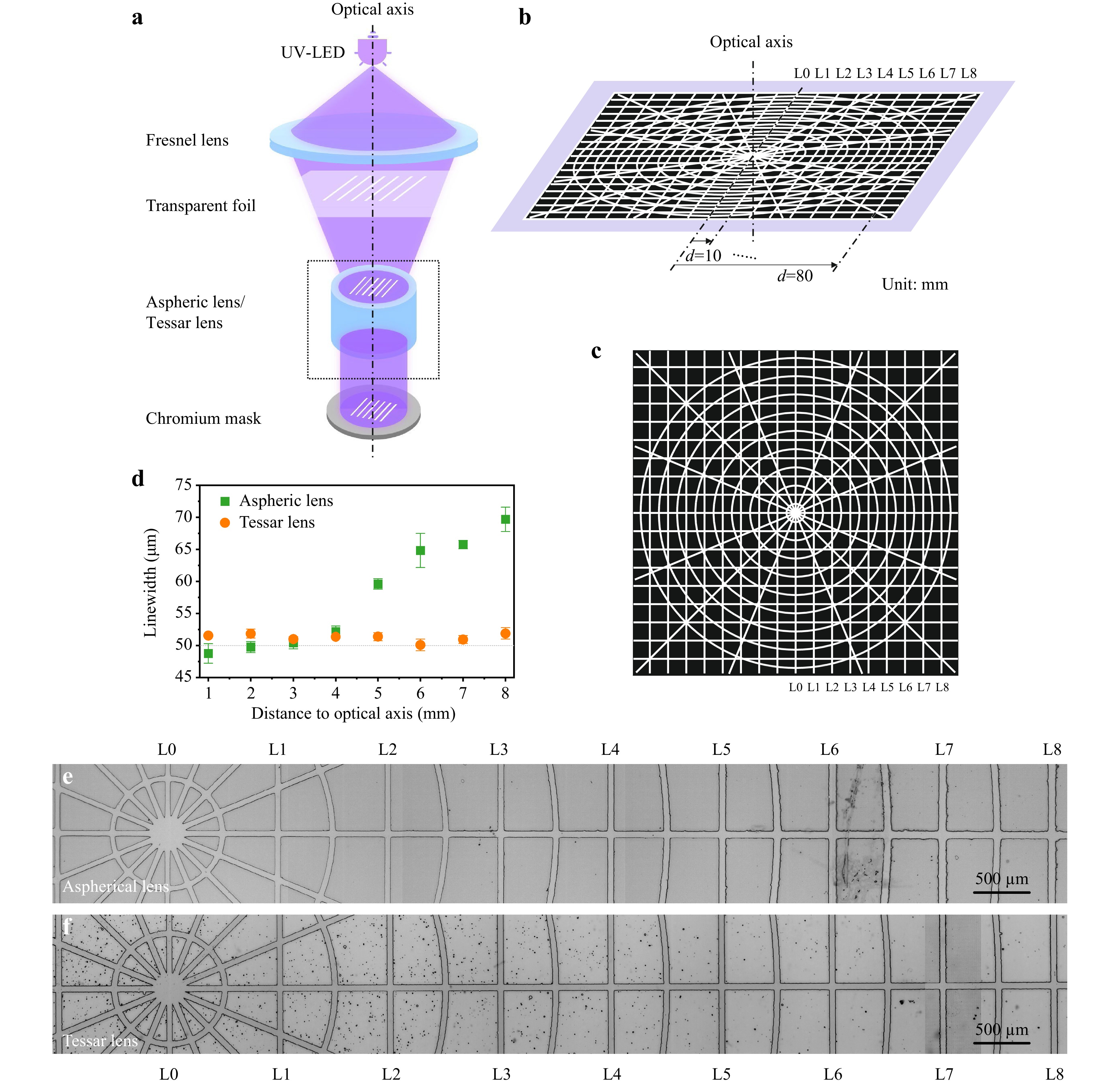
Fig. 2 Structure patterns on chromium mask layers obtained using an aspheric lens and a Tessar objective lens, respectively. An organic-inorganic hybrid photosensitive polymer was used for the structuring. a Schematic illustration of the optical setup for the preparation of the patterned chromium photomask. A high-power UV-LED was used as the light source, and a Tessar objective lens was employed as the imaging lens to minimize the field-dependent aberrations that can not be corrected by an aspheric lens. b Sketch of the printed transparent foil. c The designed structure patterns. d–f Measured widths (d) and microscope images (e–f) of lines on the chromium layer obtained using an aspheric lens and a Tessar objective lens.
As only one light wavelength is used for the photolithography process for the preparation of chromium mask in the demonstrated system, chromatic aberration can be neglected. In contrast, the spherical aberration resulting from lenses in the optical system should be considered. For high-resolution structuring it is desirable to minimize this effect. On this issue, employment of an aspheric lens instead of a convex imaging lens is usually the approach for minimization. However, this approach is not able to improve the field-dependent aberrations, which in turn could prominently affect the fabrication resolution. To correct these aberrations, a Tessar objective lens (Carl Zeiss), a well-known four-lens system enabling an imaging quality free of astigmatism and at the same time compensating the field curvature, was assembled. This lens system eliminates the field-dependent aberrations, thus ensuring a good and accurate formation of patterns onto the chromium photomask with a 10:1 demagnification in the established optical projection setup.
To investigate the improvement performance of the employed Tessar objective lens, a line array consisting of both straight and circular lines with the same linewidth of 500 µm was designed and printed on a transparent foil (see Fig. 2b). The designed pattern is shown in Fig. 2c. The straight lines are distributed with lateral distances to the center (d) increasing from 10 mm to 80 mm with a step of 10 mm. The circles are distributed symmetrically in the same manner. Their radii increase from 5 mm to 75 mm with a step of 10 mm. The printed transparent foil (Fig. 2b) was placed into the optical projection setup with its center on the optical axis of the setup. Here, the key point is to investigate and compare the performance of the aspheric lens and the Tessar objective lens in transferring patterns onto the chromium mask layer. For this purpose, an organic-inorganic hybrid photosensitive polymer36 was used and spin-coated onto the chromium layer for the investigation. Using this photopolymer, the unexposed area was washed away in the development process with the exposed area remaining on the substrate. Structure patterns on the chromium layer were prepared using both the aspheric lens and the Tessar objective lens, respectively, with the results after development process observed and compared. Here, the patterns on the chromium photomask were 10x demagnified. Eight straight lines with increasing distances of 1 mm (L1), 2 mm (L2), 3 mm (L3), 4 mm (L4), 5 mm (L5), 6 mm (L6), 7 mm (L7) and 8 mm (L8) to the structure center were considered. The measured linewidths versus distance to optical axis are displayed in Fig. 2d and microscope images of the lines obtained using both lenses are shown in Fig. 2e, f, respectively. It can be seen that the lines created using the aspheric lens exhibit larger width with the increase of the lateral distance (d) to the optical axis due to the remaining field-dependent aberrations, while the linewidth remains stably around 50 µm in the case of the Tessar objective lens, with a maximum difference of approx. 3.5% from the theoretical linewidth (50 µm). This result demonstrates the field-dependent aberrations improvement of the optical system by the use of the Tessar objective lens, which is significant toward high-resolution fabrication.
-
With the described setup configuration, a chromium mask with improved pattern quality could be obtained after the wet etching process. This patterned chromium mask was placed into the MPP setup for the subsequent structuring. In the MPP process, patterns on the chromium photomask are projected onto a photopolymer-coated substrate with a certain demagnification, which is determined by the employed microscope objective. Here, a 100x plan-apochromat oil-immersion microscope objective with a NA of 1.4 (Carl Zeiss) was used to produce a series of lines with designed widths varying from 75 nm to 975 nm with a step of 25 nm after the 1000x demagnification. With this costly plan-apochromat objective, field curvature and optical aberration caused by the objective are minimized. The already mentioned organic-inorganic hybrid photosensitive polymer36 was used and spin-coated on a glass substrate for this structuring. An overview SEM image of the fabricated lines is shown in Fig. 3a. It can be seen that all of the lines from the chromium photomask were successfully fabricated on the glass substrate. To investigate the performance of this optical fabrication setup with the use of different objective lenses, an economic 100x E-Plan oil-immersion microscope objective with a NA of 1.25 (Müller Optronics) was employed for fabrication of the same lines. An overview SEM image of the obtained lines is shown in Fig. 3b. Except for the line with a width of 75 nm, all other lines were successfully fabricated. Lines with sizes above 400 nm exhibit less sharp edges compared to those obtained by the Zeiss objective.
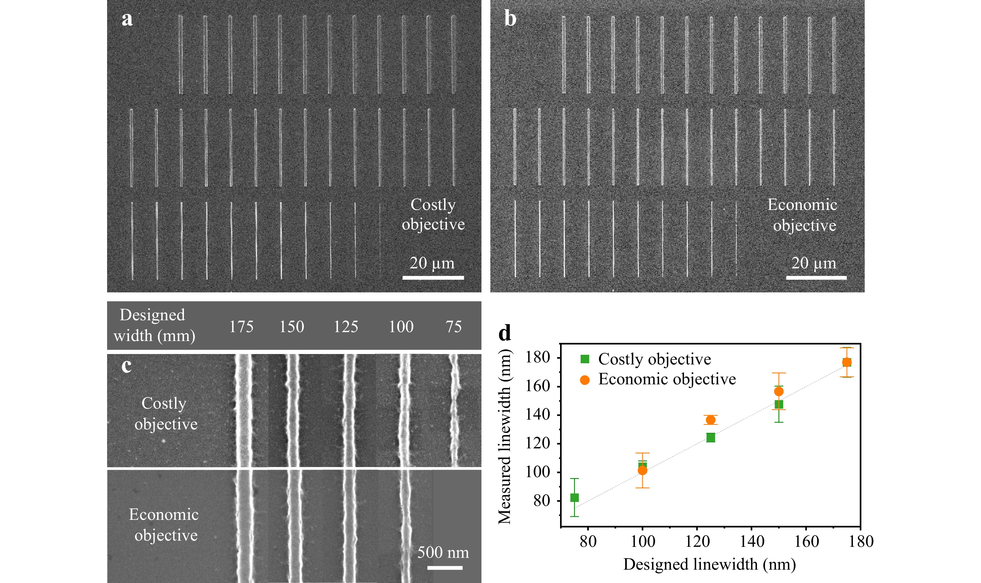
Fig. 3 Lines fabricated using different microscope objectives. a-b SEM images of lines with designed widths ranging from 75 nm to 975 nm (step: 25 nm) produced using a costly objective (a) and an economic objective (b). Both objectives were able to perform high-resolution structuring. Minimum feature sizes of 75 nm and 100 nm were realized by the costly objective and economic objective, respectively. The lines produced with the economic objective exhibits less sharp edges compared to that made by the costly microscope objective. c SEM images of produced small-featured lines with linewidths of 75 nm, 100 nm, 125 nm, 150 nm and 175 nm. d Comparison of fabricated linewidths versus designed linewidths. Lines fabricated using the economic objective is slightly broader than those made by the costly objective. Nevertheless, both objectives were able to perform high-resolution structuring.
Further comparison and analysis of downscaling fabrication by both objective lenses were performed. Fig. 3c shows detailed views of SEM images of small-featured lines (designed widths of 75 nm, 100 nm, 125 nm, 150 nm and 175 nm). It can be seen that with both objectives, lines can be projected well onto the substrate, enabling the high-quality fabrication. With the costly objective, a minimum measured feature size down to 85 nm (corresponding to a designed width of 75 nm) can be achieved, which is not enabled by the economic microscope objective. The minimum width that can be achieved with the latter is approx. 100 nm. Measured widths of the fabricated lines shown in Fig. 3c are plotted in Fig. 3d. As can be seen there, lines produced using the economic objective are in general slightly broader than those made by the costly objective. Nevertheless, feature sizes at the scale of 100 nm can be achieved by both objectives.
Furthermore, a grating structure with an area size of 100 × 100 µm, a pitch of 1 µm and a linewidth of 500 nm was also fabricated using both objectives, respectively. The gratings were made of the positive photoresist ma-P 1205 (micro resist technology). The employment of this positive photoresist indicates that the exposed area is washed away in the development process, while the unexposed area remains on the substrate, which forms the grating in the end. Fig. 4a, b display SEM images of grating structures made by the costly objective (100x, NA 1.4) and the economic objective (100x, NA 1.25), respectively. Both gratings exhibit good smoothness and the lines are distinguishable. Compared to the result shown in Fig. 4a, the grating in Fig. 4b displays a tiny defocused area at the corner (marked orange). This defocus results from the field curvature caused by the economic objective. It indicates that this economic objective has a smaller useful field of view than the costly objective. To further explore the capabilities of the proposed approach in high-resolution structuring, a non-oil-immersion objective was employed for MPP as well. The same grating was produced using a microscope objective (Carl Zeiss) with the magnification of 100x and NA of 0.95. The SEM image of the structure is shown in Fig. 4c. A very good structure formation was achieved with this objective.
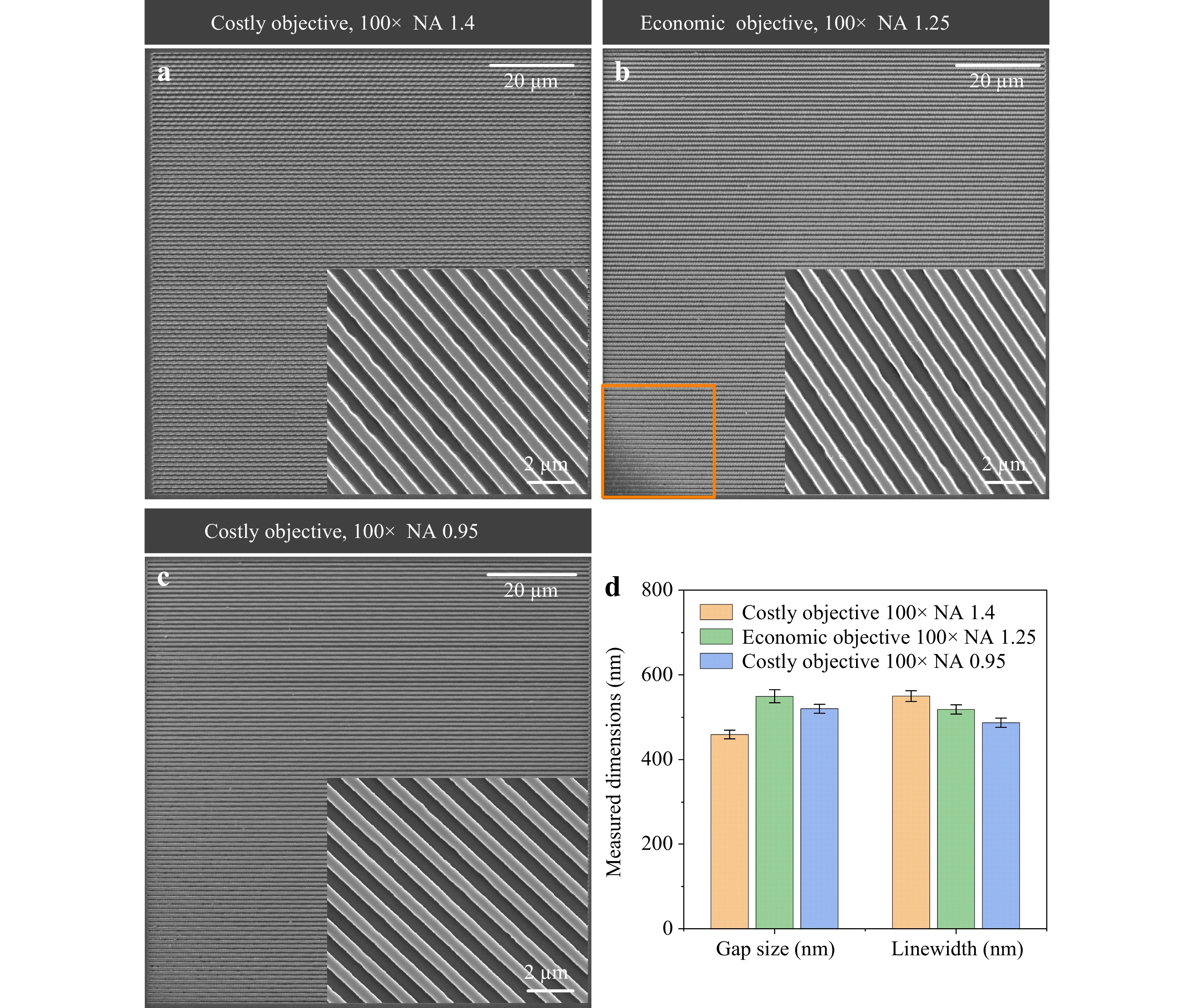
Fig. 4 Gratings fabricated using different microscope objectives. SEM images of gratings fabricated using a costly 100x objective with a NA of 1.4 (a), an economic 100x objective with a NA of 1.25 (b) and a costly 100x objective with a NA of 0.95 (c), respectively. A positive photoresist S1805 was used for the fabrication. The grating arrays produced by the costly objectives exhibit good structure formation, while the grating array obtained using the economic objective has a tiny defocused area. d Measured gap sizes and linewidths of produced gratings. The smaller gap size obtained in the case of costly 100x objective with the NA of 1.4 indicates a narrower exposure region, while the larger gap size obtained with the economic 100x objective with the NA of 1.25 reveals a wider exposure region. The costly objective with the NA of 1.4 exhibits better performance in high-resolution fabrication.
To investigate the performance of these objectives on structured size, the gap sizes between adjacent gratings lines and the linewidths of the obtained gratings were measured and compared. The measured result is plotted in Fig. 4d. The grating fabricated by the costly 100x objective with the NA of 1.4 shows the smallest gap of 459 ± 10 nm, while a lager gap (550 ± 15 nm) is obtained with the economic objective (100x, NA 1.25). The third 100x objective with the NA of 0.95 (Carl Zeiss) enables a gap size of 520 ± 10 nm. This result might be due to the better corrected chromatic aberration of the high-cost objectives compared to the economic objective. In addition, light transmission of the economic objective might also affect the structured dimension and needs to be further investigated. The measured linewidths achieved by the employed three objectives are 550 ± 12 nm (Carl Zeiss, 100x, NA 1.4), 518 ± 11 nm (Müller Optronics, 100x, NA 1.25) and 487 ± 11 nm (Carl Zeiss, 100x, NA 0.95), respectively. With a designed pitch of 1 µm, it can be seen that the costly objectives exhibit higher demagnification accuracy than the economic objective. This comparison demonstrates that the costly objectives from Carl Zeiss exhibit better performance regarding minimized field curvature and structuring resolution. In spite of this, it can still be concluded that high-resolution structures can be fabricated by both costly and economic objective lenses.
-
In this work, a highly efficient and low-cost microscope projection photolithography approach was implemented and used for micro- and nanostructuring. By optimizing the printing approach and developing optical elements with minimized field-dependent aberrations, high-resolution structures with a feature size down to 85 nm were successfully fabricated. In addition, an economic microscope objective was employed to produce high-resolution structures. A minimum feature size of approximately 100 nm was realized using this economic component. The results demonstrate the capabilities of the developed fabrication system in high-resolution fabrication. The demonstrated fabrication approach offers great potential in low-cost and highly efficient production of structures for applications in fields, i.e. optical sensing37–40, optoelectronics41,42 and nanophotonics43–45.
-
Materials used in the fabrication include the commercial positive photoresists S1805 (Shipley) and ma-P 1205 (micro resist technology), as well as a self-synthesized organic-inorganic hybrid photopolymer36. S1805 is a positive photoresist engineered for advanced integrated circuit device fabrication in wet etching and lift-off processes. It is optimized for g-line exposure and exhibits excellent adhesion and coating uniformity. In this work, this material was spin-coated on the chromium layer and structure patterns were transferred from transparent foil onto this positive photoresist layer after UV exposure. An etchant, Chrome Etch N°1 (MicroChemicals GmbH), was used in the wet etching process. The photoresist ma-P 1205 is designed for standard lithography and exhibits spectral sensitivity in the wavelength range 350-450 nm. The self-synthesized hybrid photopolymer is a low-shrinkage material designed for lithography. It exhibits a measured absorbance of approximately 32% at 365 nm in its liquid state and high transmission in the visible range.
-
The fabrication of structures is implemented by using light emitted by an UV-LED and a standard microscope objective to transfer structure patterns on a photomask to a photoresist-coated substrate. A sketch of the working principle as well as the corresponding UV lithography system is shown in Fig. 5a. This system was established using off-the-shelf standard components. A LED with a wavelength of 365 nm and output power of approx. 690 mW (Roithner LaserTechnik GmbH) was employed as the light source. Light emitted by the LED was collimated using an aspheric lens. Two tube lenses (Carl Zeiss, focal length 164.5 mm) were employed and combined with the microscope objective mounted below the beam splitter to create an infinity-corrected imaging system. This configuration is able to minimize the imaging aberrations. The first tube lens was placed above the beam splitter. A chromium photomask was placed between the convex lens and the tube lens at the position where the focal plane of the tube lens is, such that the structure patterns on the chromium photomask can be transferred onto the substrate with a minimized aberration under illumination. The other tube lens was placed between the beam splitter and CCD camera sensor, which is positioned at the focal plane of the tube lens. A substrate with spin-coated photopolymer on it was placed on a sample holder, the position of which can be controlled by moving motorized stages. To focus the substrate into the focal plane of the microscope objective, a red LED (wavelength 650 nm) was employed as the light source and an autofocus module was developed as well for easy and quick implementation of the focusing process. Depending on pattern size and resolution requirement, microscope objectives with different magnification and numerical aperture can be flexibly integrated into this system.
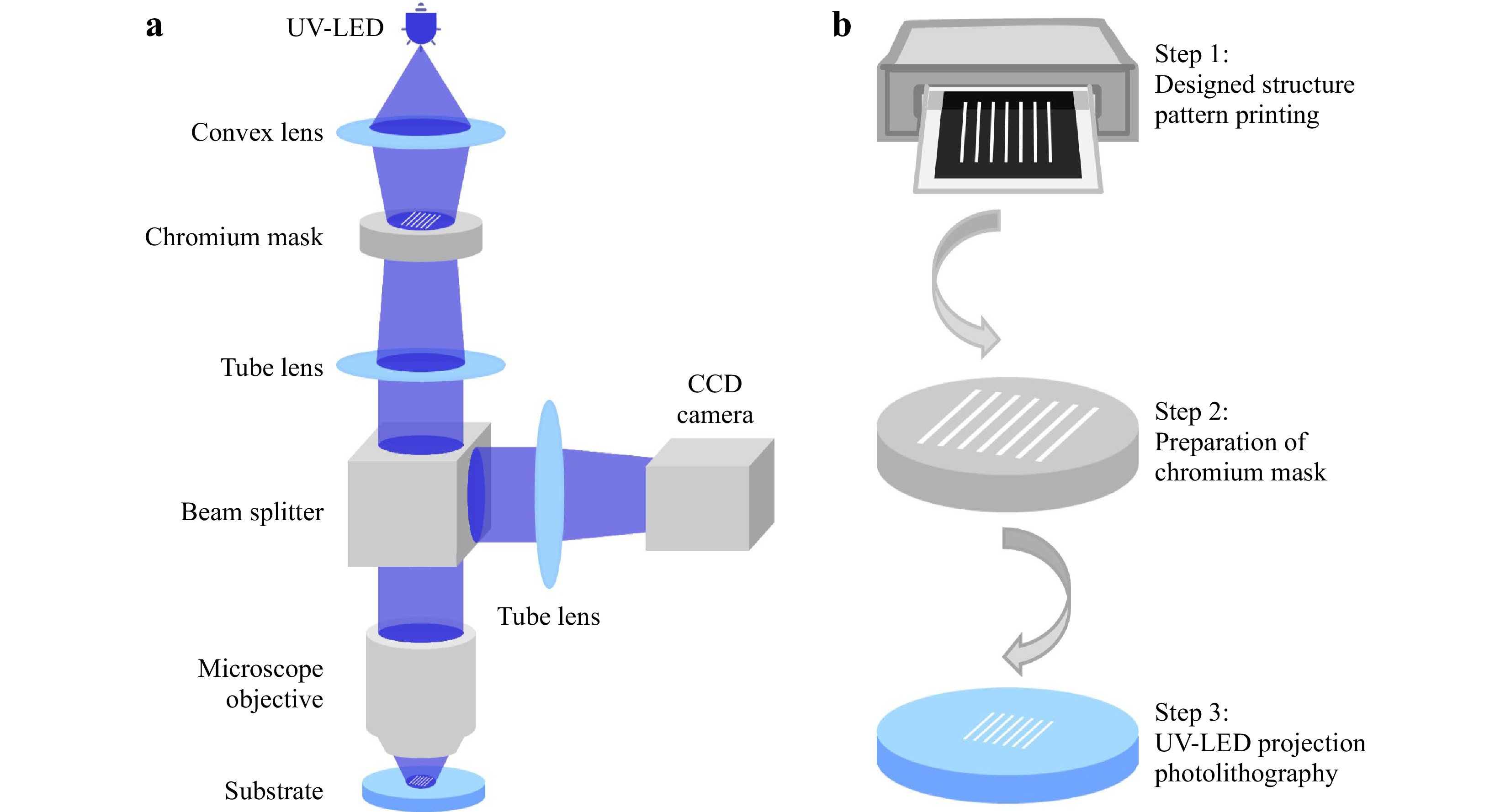
Fig. 5 Process illustrations. a Sketch of the employed UV-LED-based microscope projection photolithography. b Process chain including steps from structure design to the final projection lithography.
The fabrication of structures is realized via an established process chain, which mainly includes three steps (see the sketch in Fig. 5b): first, the desired structure pattern is designed in a vector graphic software and subsequently printed on a transparent foil using a laser plotter with a resolution of 16,256 dpi. The second step is to transfer the pattern from the foil to a chromium photomask. This is implemented using a home-built setup. A detailed description of this setup (see Fig. 2a) and the experimental investigation including process optimization can be found in the results and discussion section. With the prepared chromium photomask, the final structuring process can be implemented using the established UV-LED-based MPP system. In this step, the structure pattern projected from the photomask is focused onto the photosensitive material layer, which was spin-coated onto the substrate. Materials such as positive or negative tone photoresists, photopolymers like ormocer or homemade silica-zirconia polymer compounds can be employed in this fabrication process. The spin-coating parameters were usually taken from the processing guidelines offered by the materials manufacturers. For homemade materials, a spin-coating program with a rotation speed of 3000 rpm for 30 s was usually used. Meanwhile, the focus of the UV light on the photopolymer layer is synchronized as well. With the UV light on, the light projects structure pattern onto the material layer and the patterned photoresist area is exposed. Desired patterns were obtained with a subsequent development process.
-
The authors acknowledge the financial support from the German Research Foundation (DFG) under Germany’s Excellence Strategy within the Cluster of Excellence PhoenixD (EXC 2122, Project ID 390833453).
Feature size below 100 nm realized by UV-LED-based microscope projection photolithography
- Light: Advanced Manufacturing 4, Article number: (2023)
- Received: 14 April 2023
- Revised: 21 September 2023
- Accepted: 24 September 2023 Published online: 16 November 2023
doi: https://doi.org/10.37188/lam.2023.033
Abstract: The demand for miniaturization and integration of optical elements has fostered the development of various micro- and nanofabrication technologies. In this work, we developed a low-cost UV-LED-based microscope projection photolithography system for rapid and high-resolution fabrication. This system can be easily implemented using off-the-shelf components. It allows for micro- and nanostructuring within seconds. By optimizing the process, a minimum feature size down to approximately 85 nm was successfully realized. In addition, investigations on fabrication of the same structures using both costly and economic microscope objectives were performed. Feature sizes below 100 nm can be stably achieved. The demonstrated approach extends the technology capabilities and may find applications in fields such as nanophotonics, biophotonics sensing and material science.
Research Summary
Feature size below 100 nm realized by UV-LED-based microscope projection photolithography
The demand for miniaturization and integration of optical elements has fostered the development of fabrication technologies for high-resolution structuring. Lei Zheng from Leibniz University Hannover reported a low-cost UV-LED-based microscope projection photolithography approach towards rapid and high-resolution optical fabrication. This fabrication system can be easily established using off-the-shelf components and allows for micro- and nanostructuring within seconds. Accompanied with optimizations of the system and structuring process, a minimum feature size down to approximately 85 nm was successfully realized. In addition, fabrication of the same structures using both costly and economic microscope objectives was also implemented, with their performance compared. Feature sizes down to 100 nm can be stably achieved by the economic objective. The demonstrated approach extends the technology capabilities and may find applications in fields such as nanophotonics, biophotonics sensing and material science.
Rights and permissions
Open Access This article is licensed under a Creative Commons Attribution 4.0 International License, which permits use, sharing, adaptation, distribution and reproduction in any medium or format, as long as you give appropriate credit to the original author(s) and the source, provide a link to the Creative Commons license, and indicate if changes were made. The images or other third party material in this article are included in the article′s Creative Commons license, unless indicated otherwise in a credit line to the material. If material is not included in the article′s Creative Commons license and your intended use is not permitted by statutory regulation or exceeds the permitted use, you will need to obtain permission directly from the copyright holder. To view a copy of this license, visit http://creativecommons.org/licenses/by/4.0/.

 DownLoad: