


-
Photonic integrated circuits (PIC) are about to disrupt a variety of applications, ranging from high-speed data transmission1 and ultra-broadband signal processing2,3 to distance metrology and light detection and ranging4–7 (LiDAR) and further to chemical sensing and medical diagnostics8–12. This success largely relies on advanced wafer-level fabrication of miniaturized photonic devices that combine outstanding functionality and robustness with unprecedented performance and scalability. However, while cost-efficient mass production of PIC has become widely available through dedicated foundry services13,14, scalable photonic packaging and system assembly still represents a major challenge and an obstacle towards accelerated commercial uptake. Specifically, package-level optical chip-to-chip and fiber-to-chip connections often rely on so-called butt coupling, where device facets are brought in close proximity or even in direct physical contact to each other. This approach often requires high-precision active alignment with sub-micrometer accuracy, thereby complicating assembly processes. Moreover, matching of the mode fields can represent a challenge, in particular when connecting waveguides with vastly different refractive-index contrasts. This challenge may be overcome by coupling of devices via intermediate discrete optical components such as ball lenses15 or graded-index (GRIN) structures16–18. While this approach increases the design flexibility and opens a path towards integrating free-space optical elements such as polarization beam splitters or optical isolators19 into the beam paths between optical chips, it renders the assembly process even more complex by increasing the number of components that have to be aligned. There is hence a strong need for scalable and flexible packaging concepts that can complement wafer-level mass fabrication of the underlying PIC.
In this paper, we show that 3D-printed facet-attached microlenses (FaML) offer an attractive option for advanced photonic system assembly. FaML can be printed with high precision to the facets of optical components20 using multi-photon lithography, thereby offering the possibility to shape the emitted beams by freely designed refractive or reflective surfaces. Specifically, the emitted beams can be collimated to a comparatively large diameter that is independent of the device-specific mode fields. This relaxes both axial and lateral alignment tolerances to the extent that costly active alignment becomes obsolete and can be replaced by passive15,21 assembly techniques based on machine vision and/or simple mechanical stops. Moreover, in contrast to direct butt coupling, the FaML concept opens the possibility to insert discrete optical elements such as optical isolators into the free-space beam paths between PIC facets. Building upon our previous work20, we show the viability and the versatility of the scheme in a series of selected demonstrations of high technical relevance. In a first set of experiments, we couple fiber arrays to arrays of edge-coupled silicon photonic (SiP) chips, reaching insertion losses of 1.4 dB per interface with a translational lateral 1 dB alignment tolerance of ±6 µm. To the best of our knowledge, this is the lowest loss so far demonstrated for an edge-emitting SiP waveguide interface with micron-scale alignment tolerances. We also demonstrate that the outstanding alignment tolerance of our scheme allows for contactless pluggable fiber-chip interfaces using conventional injection-molded parts such as a LEGO brick for detachable mechanical connections. In a second set of experiments, we demonstrate free-space transmission over distances in the mm-range, using standard machine-vision techniques for alignment. In this experiment, we further insert a discrete optical polarization beam splitter into the beam path between a single-mode fiber (SMF) array and array of edge-coupled indium-phosphide (InP) photodetectors. A third set of experiments is dedicated to interfaces between InP lasers and SMF arrays. In this context, we demonstrate coupling with ultra-low back-reflection by connecting planar devices through non-planar beam paths that only comprise tilted optical surfaces. We estimate only −44 dB of spurious back-reflection, comparable to the levels achieved via advanced lensed fibers with anti-reflection (AR) coating. Based on these exemplary demonstrations of the outstanding versatility of FaML-based assembly concept, we believe that the concept opens an attractive path towards advanced photonic system assembly that may overcome most of the current challenges.
-
The concept of using facet-attached microlenses (FaML) for assembly of integrated optical systems is illustrated in Fig. 1, which shows an exemplary case for an optical transmitter consisting of an array of InP lasers with angled facets, an optical isolator block, and an array of modulators on a silicon-photonic (SiP) chip. The output of the SiP chip is connected to a pluggable array of single-mode fibers (SMF) in a mechanical transfer (MT) ferrule, which is positioned by mechanical alignment pins. The Insets (i), (ii), and (iii) show magnified views of different free-form FaML, which can be designed to collimate the free-space beams to diameters of up to 60 µm, thereby greatly relaxing translational alignment tolerances. Inset (i) shows the schematic of a FaML assembly printed to the facet of an angled edge-emitting InP laser. The FaML assembly consists of a free-form lens and a prism, which jointly expand, collimate and redirect the beam. The angled plane surfaces and the strongly curved lens surface reduce unwanted back-reflections into the laser cavity. Insets (ii) and (iii) show schematics of other FaML, which are printed to the facet of an edge-coupled SiP chip and to the facets of SMF, respectively.
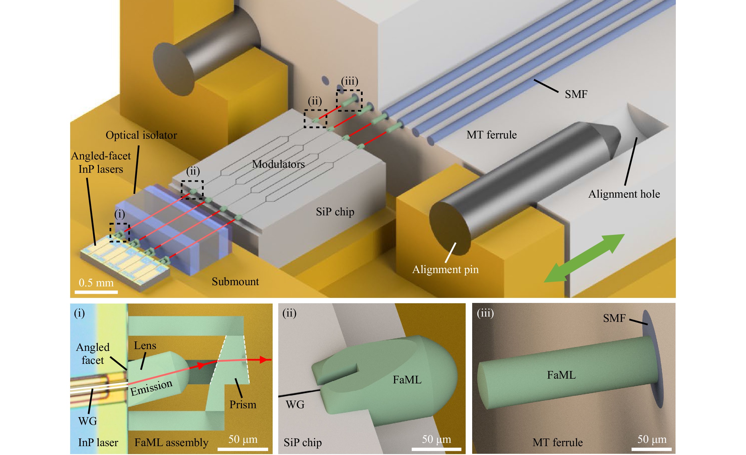
Fig. 1 Illustration of an optical assembly based on 3D-printed facet-attached microlenses (FaML). The assembly consists of an array of angled-facet InP lasers, an optical isolator block, and a silicon photonic (SiP) chip with an array of modulators. The output of the SiP chip is connected to an array of single-mode fibers (SMF) in a mechanical transfer (MT) ferrule. The ferrule is part of a pluggable connector (green arrow) and is positioned by mechanical alignment pins. Free-form FaML on each facet, Insets (i), (ii), and (iii), expand and match the mode fields of the different components, and enable low-loss coupling with relaxed alignment tolerances. Inset (i): Schematic of a FaML assembly printed to the facet of an angled edge-emitting InP laser. An assembly with a free-form lens and a prism expands, collimates and redirects the beam. The angled plane surfaces and the strongly curved lens keep parasitic back-reflections into the laser cavity minimal. Insets (ii) and (iii): Schematic of free-form FaML, printed to the facet of an edge-coupled SiP chip and to the facet of a SMF, respectively. These FaML can be designed to collimate the free-space beams to diameters of up to 60 µm, thereby greatly relaxing translational alignment tolerances and enabling highly reproducible pluggable connections.
The concept shown in Fig. 1 illustrates four key functionalities that are generic for advanced optical assemblies: Redirection of beams emitted by arrays of angled-facet lasers, which is key to efficient coupling of such lasers to device arrays with standard facet-normal emission, optical coupling over mm-scale distances, which allows for insertion of discrete micro-optical elements such as isolators into the free-space beam paths, low-loss coupling to arrays of edge-emitting SiP chips with relaxed alignment tolerances, as well as assembly by passive positioning and pluggable optical connections, that allow for reproducible low-loss coupling to PIC facets based on mechanical alignment structures. In the following sections, we describe a series of proof-of-concept experiments that demonstrate these generic functionalities using FaML in different settings involving SiP chips, active and passive InP dies, as well as single-mode fiber arrays.
-
In our first set of experiments we demonstrate low-loss coupling to edge-emitting SiP chips as well as pluggable optical connections based on simple mechanical alignment structures. To this end, we print an array of FaML to the edge of a SiP chip and investigate the coupling efficiency to an array of lensed single-mode fibers (SMF) along with the associated alignment tolerances. We further highlight the benefit of relaxed alignment tolerances by demonstrating pluggable fiber-chip connections based on a pair of off-the-shelf injection-molded LEGO® bricks. For our experiments, we use standard SMF arrays and SiP chips, which contain inverse-tapered edge couplers (EC), arranged in a loopback-configuration with a pitch of 127 µm, see Fig. 2. Details on the SiP chips can be found in the Materials and Methods. Using multi-photon lithography, we 3D-print FaML directly to the facets of the SiP chip and the fiber array (FA), see Insets (i) and (ii) of Fig. 2, targeting an expanded mode-field diameter (MFD) of 25 µm. In this work, the MFD is defined as diameter of the contour line at which the intensity profile has decayed to 1/e2 (13.5%) of the value of its maximum. We measure the spots generated by the FaML using an IR microscope, see Supplementary Section 1 for details. When coupling 1550 nm-light to the SMF, the lenses produce round spots with a consistent MFD of 25 µm at a distance of 150 µm from the lens apex, as expected. For the FaML attached to the SiP chip, the measured spots turn out to be slightly elliptical with a size of 25 µm × 20 µm at a distance of 280 µm away from the lens apex, i.e., the extension in the vertical direction is slightly smaller than designed.
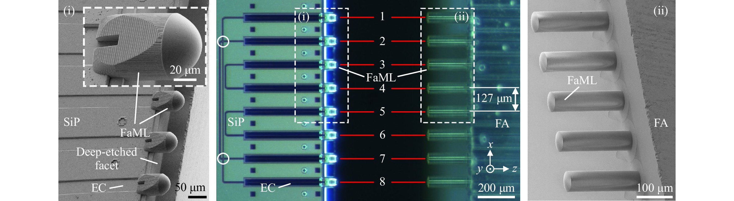
Fig. 2 Coupling between a single-mode fiber array (FA) and an array of edge-emitting SiP waveguides using 3D-printed facet-attached microlenses (FaML, microscope image in the center). The Insets (i) and (ii) to the left and to the right show magnified scanning electron microscope (SEM) images of the FaML on the SiP and FA sides, respectively. The SiP chip contains waveguides that arranged in a loopback-configuration with a pitch of 127 µm and that are terminated by tapered edge couplers (EC). The outer loopbacks contain a pair of waveguide crossings, marked by the white circles, that have been optimized for operation in TE polarization. We conduct coupling experiments with the chip fixed in place and the fiber array (FA) mounted on a six-axis stage. First, light at a wavelength of 1550 nm is coupled into the fiber of Channel 1, and the output power is recorded at the loopback Channel 8. For the coupling, all degrees of freedom of the six-axis stage are used to maximize the signal of the Loopback (1, 8). After that, the signals through the other Loopbacks (2, 7), (3, 4) and (5, 6) are simultaneously measured, resulting in an average loss of 1.44 dB per fiber-chip interface for TE-polarized light, see Table 1. The fiber array is then moved with respect to the fixed SiP chip to extract the lateral and angular alignment tolerances, see Fig. 3.
To characterize the performance of the FaML-based interfaces we conduct coupling experiments with the chip fixed in place and the FA mounted on a six-axis positioning stage. First, light at a wavelength of 1550 nm is coupled into the fiber of Channel 1, and the output power is recorded at the loopback Channel 8, see Fig. 2. In this step, we use quasi-TE polarization, having a dominant electric field component parallel to the substrate of the SiP chip. We optimize all six degrees of freedom of the stage to achieve maximum received power after the Loopback (1, 8). We then keep the position and measure the signals through the other Loopbacks (2, 7), (3, 4) and (5, 6). Assuming that both fiber-chip interfaces in each loopback have the same performance, we estimate the coupling losses per interface, each comprising a pair of FaML and a waveguide-based edge coupler (EC) on the SiP chip. The results for the four loopbacks are very uniform with an average value of 1.44 dB, see Table 1, which represents a significant improvement to our previous results22 of 4 dB. The numbers given are obtained after correction for on-chip losses, see Materials and Methods. Using 3D-printed microlenses without anti-reflection coating, we cannot avoid Fresnel reflection at the two lens surfaces, which amount to a total of approximately 0.4 dB, estimated for perpendicular incidence and a refractive index of the lens material (VanCore A, Vanguard Automation GmbH) of n = 1.53. The remaining loss of approximately 1.0 dB is attributed to transition losses within the EC and to mode mismatch. We also repeated the same measurement for quasi-TM polarization, having a dominant magnetic field component parallel to the substrate. Note that the Loopbacks (1, 8) and (2, 7) contain two waveguide crossings each, indicated by white circles in Fig. 2, which were designed only for TE polarization and thus prevent a measurement of these loopbacks in TM-polarization. For the remaining Loopbacks (3, 4) and (5, 6), we find a loss of 2.2 dB per fiber-chip interface in TM-polarization. This value is slightly larger than for TE-polarization due to polarization-dependent loss (PDL) of the edge-coupler transition as specified in the Process Design Kit of the associated foundry, see Materials and Methods.
TE loopback path (1, 8) (2, 7) (3, 4) (5, 6) avg. Loss per fiber-chip interface [dB] 1.46 1.43 1.45 1.40 1.44 Table 1. Losses for simultaneous coupling of 8 channels from a fiber array to a SiP-chip after active alignment.
Besides low coupling losses, the translational and rotational alignment tolerances are of key importance for highly scalable packaging processes. To investigate this aspect, we switch back to quasi-TE polarization and first extract the translational lateral alignment tolerance by moving the fiber array in the (x, y)-plane perpendicular to the fiber axis, see Fig. 2, while recording the output power of Loopback (1, 8). In this experiment, the angular orientation of the fiber is kept as previously optimized. Fig. 3a shows the excess coupling loss per fiber-chip interface as a function of the lateral misalignment. The dashed-dotted red circle with radius of 6 µm indicates the theoretical 1 dB coupling tolerance for a Gaussian beam with an MFD of 25 µm, see Supplementary Section 2.5, which is in excellent agreement with measured data. Note that the slightly asymmetric spot generated by the FaML on the SiP side results in a hardly noticeable asymmetry of the measured 1 dB contour line.
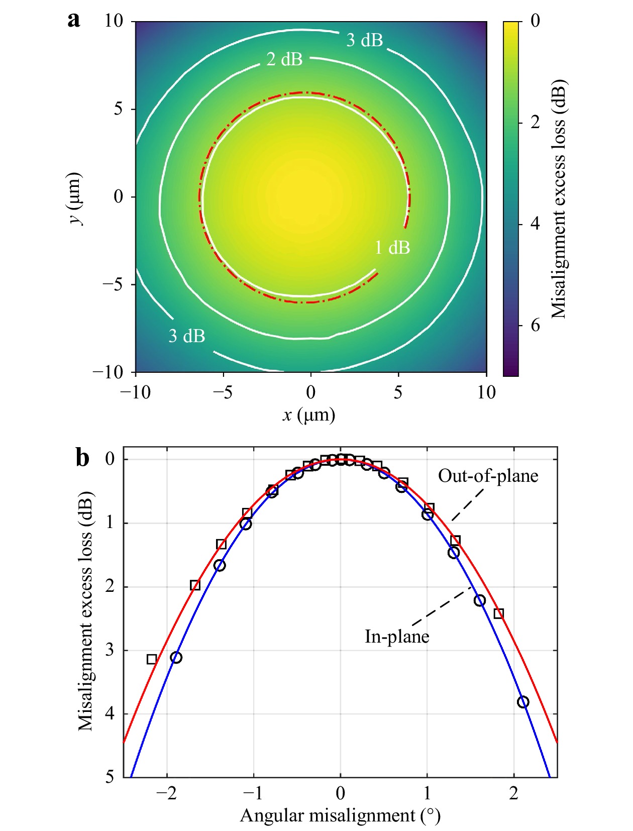
Fig. 3 Relative power loss for translational lateral and for rotational misalignment of the FaML-based coupling interface between the SMF-array and the SiP chip shown in Fig. 2. The depicted values refer to the loss per coupling interface in Loopback (1, 8), where each interface comprises an FaML pair and an EC, see Fig. 2. The optimum position corresponds to a coupling loss of 1.46 dB, see Table 1. a Translational lateral alignment tolerances in the (x, y)-plane of Fig. 2. The 1 dB tolerance amounts 6 µm in the radial direction and corresponds to the predicted contour line for a Gaussian beam with a MFD of 25 µm (red dash-dotted circle), see Supplementary Section 2.5. b Rotational (angular) tolerances measured for an in-plane rotation (circles, rotation in the (x, z)-plane of Fig. 2) and for an out-of-plane tilt (squares, rotation in the (y, z)-plane of Fig. 2). The solid lines represent a fit based on a Gaussian-beam model, leading to a beam waist diameter of 25 µm and 23 µm for the in-plane and the out-of-plane data, respectively. The model function can be found in Supplementary Section 2.2.
For measuring the angular alignment tolerances, Fig. 3b, the fiber array is rotated, followed by a pivot-point correction of rotation-induced translation and a measurement of the transmission through Loopback (1, 8). We record data points for a rotation in the (x, z)-plane of Fig. 2 (in-plane rotation, circles in Fig. 3b), as well as a for a rotation in the (y, z)-plane (out-of-plane tilt, squares in Fig. 3b). The solid lines in Fig. 3b show fits of the rotational coupling tolerance based on a Gaussian beam model according to Supplementary Section 2.2. In case of the in-plane rotation, the fit corresponds to a beam waist diameter of 25 µm, well in line with the lens design. For the out-of-plane tilt, the fit corresponds to a slightly smaller beam waist diameter of only 23 µm, which is consistent with the fact the spot generated by the lens on the SiP side was indeed slightly smaller in the vertical direction than in the horizontal direction. In summary, we find a translational 1 dB alignment tolerance of 6 µm in the radial direction and a rotational alignment tolerance of 1.1°. Note that translational and rotational tolerances are subject to a fundamental trade-off, see Supplementary Section 2, in particular Supplementary Fig. S3. Note also that translational misalignment in the axial direction, see Supplementary Section 2.3, is usually not crucial if beam-expanding FaML pairs are used, with typical 1 dB-alignment tolerances of hundreds20 of micrometers or even more.
For coupling of waveguide and fiber arrays, one would expect a slight deviation of the optimum coupling positions for the various channels. To investigate this aspect, we return to the previous optimum fiber-array position and orientation for Loopback (1, 8) and move the fiber array laterally while measuring the power transmission through the various loopbacks. In this measurement, we keep the angular alignment of the fiber array fixed. We find that the optimum positions for the various loopbacks deviate by less than 1 µm, mainly in the horizontal x-direction. This confirms the high precision of the fabricated FaML, given the fact that the spacing of the fibers within the array is specified by the manufacturer with an accuracy of ±0.3 µm23,24. Note that the excess loss associated with sub-1 µm transverse misalignments is negligible for a MFD of 25 µm, translating into an excess loss of less than 0.05 dB per FaML pair, see Supplementary Section 2.5.
Finally, we investigate the uniformity of the emission direction of the various FaML. To this end, we individually maximize the transmission of each of the Loopbacks (2, 7), (3, 4), and (5, 6) by optimizing the position and the orientation of the fiber array in all six degrees of freedom. In the respective optimum positions and orientations, we then compare the fiber axis rotation angles
${R_{x, y, z}}$ to the ones previously found when optimizing the signal to the Loopback (1, 8). We find that the individual optimum angles are highly consistent, making it impossible to measure any deviations within the measurement accuracy of$ \pm 0.05^\circ $ of our six-axis stage. This highly reproducible emission direction of the individual FaML is of utmost importance when aligning waveguide and fiber arrays, in particular when bigger distances in the millimeter-scale need to be bridged to allow for inserting of discrete micro-optical elements, see Fig. 1. In this context, automated fabrication of FaML with high alignment precision to on-chip structures is key to achieve the necessary reproducibility, see Materials and Methods for details.The alignment tolerances of FaML-based optical coupling interfaces, Fig. 3, can be met by high-precision of injection-molded plastic parts that can be mass-produced at low cost. We demonstrate this by building a pluggable connection based on off-the-shelf LEGO bricks – in analogy to Reference25, where a similar fiber-to-chip connection has been built for surface coupling using a combination of grating couplers and discrete fused-silica microlenses. Fig. 4a shows a schematic view of our assembly. The LEGO connection consists of a fixed (yellow) brick and a removable (dark transparent) brick with an attached plane aluminum cover plate (grey). The SiP chip is glued on the submount first, and the FA is subsequently aligned actively and glued onto the cover plate on the right-hand side, while the LEGO bricks are stuck together. No significant drift is observed while curing the UV glue, see Materials and Methods. Finally, the insertion loss is measured after disassembling and re-establishing the LEGO connection for a total of N = 50 times. The mean transmission per connection amounts to
$\bar \eta = 0.65$ with a standard deviation of${\sigma _\eta } = 0.08$ . The interval$\bar \eta \pm {\sigma _\eta }$ corresponds to losses between 1.41 dB and 2.46 dB, with a mean loss of 1.9 dB, see Fig. 4c. This is approximately 0.5 dB higher than the value initially found with active alignment, see Table 1, but still lower than the mean losses of the pluggable connection demonstrated in Reference25, which additionally required separate active alignment of the fused-silica lenses with respect to the fiber array and with respect to the on-chip grating couplers.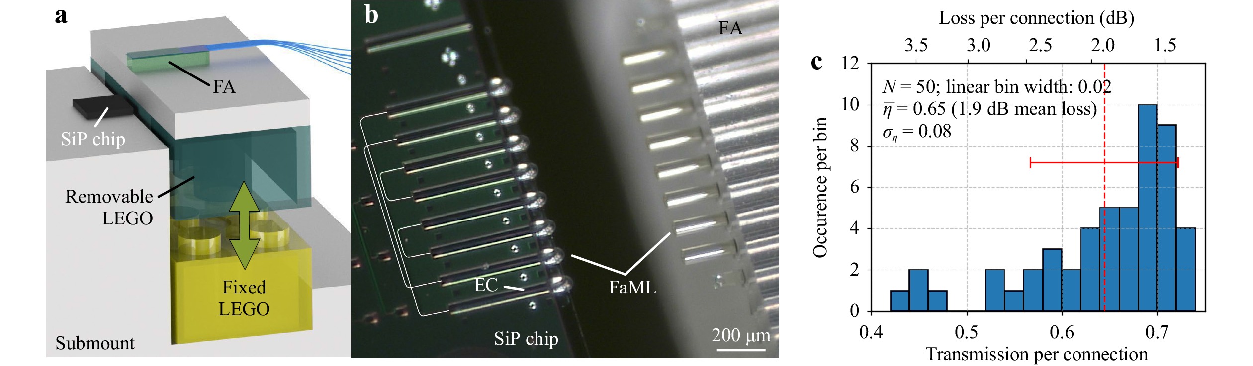
Fig. 4 Pluggable single-mode fiber-chip connection using FaML and plastic injection-molded LEGO bricks. a Schematic view of the assembly. The LEGO-plug consists of a fixed (yellow) brick and a removable (dark, transparent) brick with an attached plane cover plate (grey). The direction of separation and reconnection is indicated by a green double arrow. The silicon photonic (SiP) chip is glued on the submount first, and the fiber array (FA) is subsequently aligned actively and glued onto the removable part, with the LEGO bricks stuck together. No significant drift is observed while curing the UV-glue. Finally, the insertion loss is measured after breaking and re-establishing the connection, indicated by the green arrow. b Zoom-in of the FaML-based optical interconnects. c Histogram of measured power transmission factors per fiber-chip interface, each comprising an FaML pair and a tapered edge coupler (EC), see Fig. 2. The connection was re-plugged N = 50 times, and the histogram is shown with a linear binning of the power transmission factor η with a bin width of 0.02. The mean transmission per connection amounts to
$\overline \eta $ = 0.65 with a standard deviation of σn = 0.08. The interval$\overline \eta \pm \sigma_n $ corresponds to losses between 1.41 dB and 2.46 dB around a mean loss of 1.9 dB, about 0.5 dB higher than the value found with active alignment, see Table 1. The mean loss is indicated by a vertical dashed red line, and the corresponding error bar represents the standard deviation ±σn.We furthermore measure the spectral bandwidth of our FaML-based fiber-chip interfaces, see Fig. 5. The depicted transmission again refers to one coupling interface, comprising an FaML pair as well as an EC, see Fig. 2. The waveguide loss specified by the foundry for a wavelength of 1550 nm was subtracted. We find a noticeable wavelength-dependence and clear differences between TE and TM polarization, which we attribute to the transmission characteristics of the EC rather than to the FaML. We confirm this notion by simulating the wavelength dependence of the FaML, which would lead to variations of the coupling efficiency well below 0.1 dB within the wavelength range used in our measurements. The 1 dB bandwidth significantly exceeds the 150 nm tuning range of our laser sources both for TE and TM polarization. Independently of the polarization, the transmission is virtually flat (±0.1 dB) within the C-band (1530 nm to 1570 nm, blue shaded region in Fig. 5).
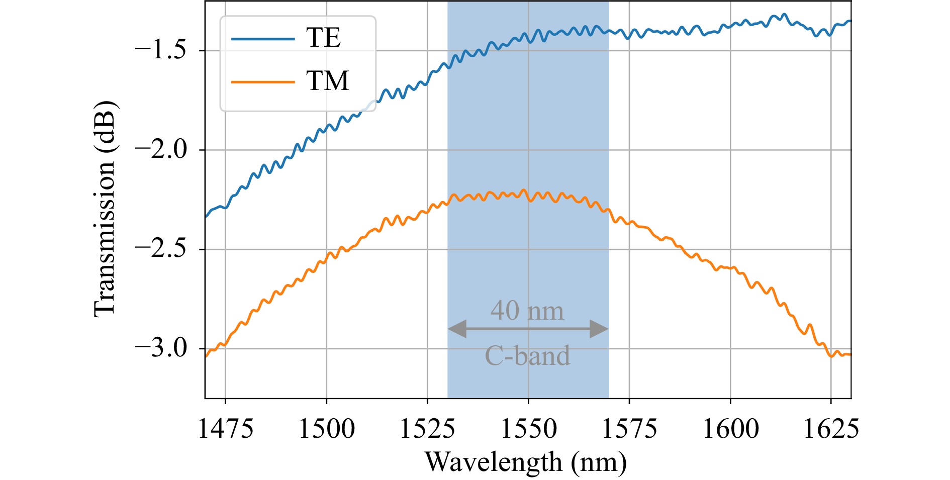
Fig. 5 Measured wavelength-dependent transmission per fiber-chip interface, each including a FaML pair and an EC, see Fig. 2. We attribute the noticeable wavelength dependence and the differences between TE and TM polarization to the transmission characteristics of the tapered edge coupler (EC) – the wavelength dependence of the FaML would lead to variations of the coupling efficiency well below 0.1 dB within the wavelength range used in our measurements. Still, the 1 dB bandwidth significantly exceeds the 150 nm tuning range of our laser sources.
-
In the previous section, the FaML were designed to produce a beam-waist diameter of 25 µm, presenting a good trade-off between translational and rotational alignment tolerances, see Supplementary Section 2.7 for details. Clearly, the structures can be designed to produce even larger beam diameters, thereby reducing the beam divergence. This allows for large, e.g., mm-scale distances between the FaML of the associated coupling interface, such that discrete micro-optical components such as optical isolators can be inserted in the beam paths between optical chips, see Fig. 1. At the same time, larger beam diameters further relax the translational alignment tolerances at the expense of their rotational counterparts. In the following, we describe our proof-of-concept demonstrations related to large-distance optical coupling with and without intermediate micro-optical elements.
For our experiments, we use standard SMF arrays and edge-coupled InP photodiode arrays (PDA, Finisar / II-VI Inc.). We 3D-print FaML to the fiber array (FA), Inset (i) of Fig. 6a, and to the PDA chip, Inset (ii) of Fig. 6a. With these components, we demonstrate a passive SMF-array-to-chip assembly with a free-space coupling distance as large as 3.3 mm. The lenses on the FA transform the SMF mode-field diameters of 10 µm to a free-space Gaussian beam having a waist of 60 µm diameter at a distance of 1.65 mm from the FaML apex, i.e., in the center of the free-space beam path. The PDA chip was designed for butt-coupling to SMF, containing an on-chip tapered spot-size converter that produces a MFD of 10 µm at the chip facet. We print lenses to the chip having the same optical design as those printed to the FA, transforming an incoming Gaussian beam with a waist diameter of 60 µm to a Gaussian spot with a 10 µm diameter at the PDA chip facet.
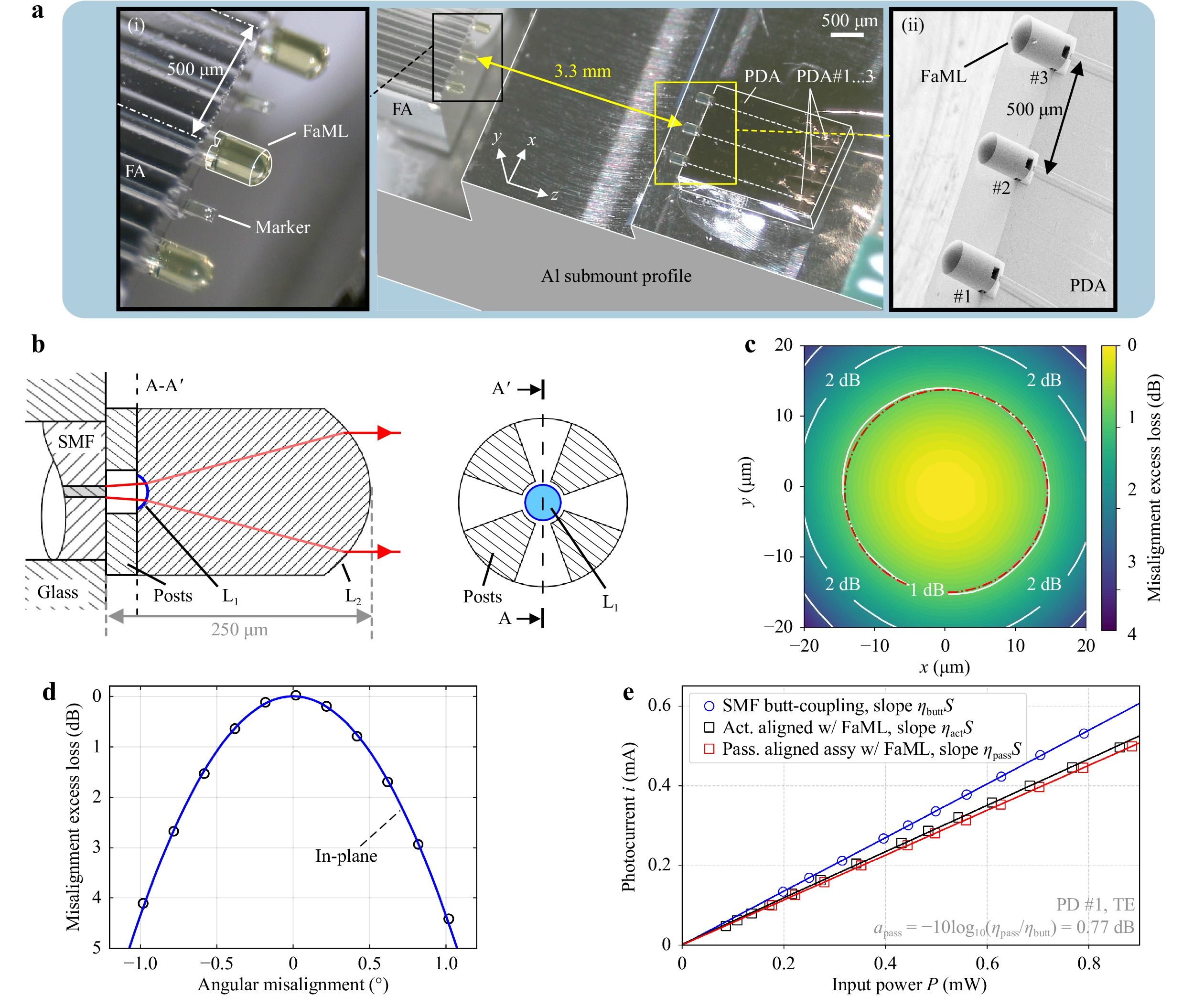
Fig. 6 Passively aligned assembly using FaML for coupling over large distances. In a proof-of-concept experiment, we couple a single-mode fiber array (FA) to an InP photodiode array (PDA) over a free-space distance of 3.3 mm, which allows for inserting optical components such as beam splitters or optical isolators into the beam path, see Fig. 1 and Fig. 7. a Three fibers of the fiber array (FA), Inset (i), are coupled to three waveguides leading to the photodiodes PD#1, #2, #3 of an edge-coupled InP photodiode array (PDA), Inset (ii). Fiber cores and on-chip waveguides are illustrated by dashed lines. FaML are printed to the facets of the FA and the PDA chip. In the assembly process, we first glue the lensed PDA chip to an aluminum submount and then align the lensed FA passively using an automated assembly machine (ficonTEC Service GmbH), see Materials and Methods as well as Supplementary Section 3 for details. The aligned components are fixed with a UV-curable glue. Printed alignment markers help with the detection of the FA during the assembly process, see Inset (i) and Supplementary Section 3 for details. b Design drawing of the FaML on the FA side. The FA end-faces are flush with the embedding glass block. The body of the lens sits on four posts with a small air gap between the waveguide end-face and the first refractive surface of the lens, see cross section along the line A–A’ sketched on the right. This lens surface is concave (L1, highlighted in blue) and increases the divergence of the beam. The second lens surface (L2) is convex and collimates the beam. Both surfaces form a Galilean telescope, which enlarges the SMF mode field diameter (MFD) of 10 µm to a beam waist diameter of 60 µm over the shortest possible axial distance. The choice of the expanded beam diameter considers tolerances of the 3D-printing and of the passive assembly processes. The original PDA chip is designed for butt-coupling using SMF with a MFD of 10 µm. We therefore use the same optical lens design as for the FA. c Relative loss for a translational lateral shift of the FA with respect to the optimum position. The 1 dB tolerance amounts to 14.4 µm in radial direction and corresponds fairly well to the predicted contour line for a coupling loss of 1 dB calculated for a Gaussian beam with a MFD of 60 µm (red dash-dotted circle), see Supplementary Section 2.5 for the underlying model. d Measured excess loss for an in-plane rotation in the (x, z)-plane of the FA with respect to the PDA. The rotational 1 dB tolerance amounts to 0.48° only and corresponds to the predicted coupling loss for a Gaussian beam with a MFD of 57 µm (blue line), see Supplementary Section 2.2 for the underlying model. e Power dependent photocurrent
$i=S \times (\eta P) $ of PD#1 in TE polarization in different stages of the assembly experiment: Blue circles refer to a measurement prior to printing the FaML using SMF butt-coupling with coupling efficiency$\eta_{\rm{butt}} $ , black open squares give the results for active alignment after printing the FaML (no glue, coupling efficiency$\eta_{\rm{act}} $ ), and red squares refer to passive alignment using the automated assembly machine (FA fixed with glue, coupling efficiency$\eta_{\rm{pass}} $ ). The measurements confirm that FaML allow for low-loss coupling via passive alignment without any performance penalty compared to active alignment. The excess alignment loss$a_{\rm{pass}}=-10\log_{10}(\eta_{\rm{pass}}/\eta_{\rm{butt}}) $ amounts to only 0.77 dB.The lens design for the FA is shown in Fig. 6b. The FA end-faces are flush with the embedding glass block. The body of the lens sits on four posts with a small air gap between the waveguide end-face and the first refractive surface of the lens. This lens surface is concave (L1, highlighted in blue) and increases the divergence of the beam. The second lens surface (L2) is convex and collimates the beam. Both surfaces form a Galilean telescope which enlarges the incoming beam diameter at the shortest possible axial distance. The PDA lens follows the same design.
In the assembly process, we first glue the lensed PDA chip to an aluminum submount and then align the lensed FA passively with a custom assembly machine (ficonTEC Service GmbH, see Materials and Methods, and Supplementary Section 3 for details). The aligned FA is fixed with glue. The three waveguides leading to the photodiodes PD#1, #2, #3 on the PDA chip are spaced by 500 µm, while the FA has a pitch of 250 µm. We therefore print a lens on every second fiber of the FA only, while the remaining fiber facets are used for printing alignment markers for the passive assembly process, see Inset (i) of Fig. 6a and Supplementary Section 3 for details.
The choice of the expanded beam diameter of 60 µm is a compromise and considers the tolerances of the passive assembly process. In particular, the measurement of the orientation of the FA and the PDA relies on detecting the edges of these objects by machine vision and is thus subject to measurement errors, which could lead to misalignment in the assembly process. The resulting beam-pointing error leads to a coupling loss which is the smaller the larger the mode field diameter becomes. However, too large a mode field diameter leads to a low tolerance with respect to an angular misalignment. These considerations specific to passive alignment are elaborated in Supple-mentary Section 2.8. The measured excess loss for a translational lateral shift of the FA with respect to the optimum position is shown in Fig. 6c. The 1 dB tolerance amounts to 14.4 µm in the radial direction and corresponds to the predicted contour line for a Gaussian beam with a MFD of 60 µm, indicated by a red dash-dotted circle in Fig. 6c, see Supplementary Section 2.5 for the underlying model. The measured excess loss for an in-plane rotation in the (x, z)-plane of Fig. 6a is given by the black circles in Fig. 6d. The rotational 1 dB tolerance amounts to 0.48° only and corresponds to the predicted coupling loss for a Gaussian beam with a MFD of 57 µm (blue line), see Supplementary Section 2.2 for the corresponding model.
To quantify the absolute losses of the coupling interface, we measure the photocurrents
$ i = S \times (\eta P) $ at different stages of the assembly process while varying the input power into the associated SMF, see Fig. 6e for results obtained from PD#1 in TE polarization. In a first stage, we butt-couple an SMF to the PDA chip facet and measure the photocurrents of PD#1, #2, #3 – the results for TE-polarized light (dominant electric field components parallel to the substrate plane) coupled to PD#1 are indicated by blue circles in Fig. 6e. This measurement and the associated coupling efficiency${\eta _{{\text{butt}}}}$ is used as a baseline for the subsequent experiments. We then print the lenses both on the FA and the PDA, adjust the alignment for PD#1, #2, #3 actively, and again record the photocurrents, black squares, leading to the coupling efficiency${\eta _{{\text{act}}}}$ . In the third stage, we use an automated procedure to passively align height, lateral position, and tilt of the FA, which is then fixed with glue applied to the edges of the glass block. The measurement results are indicated by red squares in Fig. 6e, leading to the coupling efficiency${\eta _{{\text{pass}}}}$ . Within the measurement uncertainty of ±3%, the coupling efficiencies$\eta_{\rm{act}} $ and$\eta_{\rm{pass}} $ do not differ. This is the consequence of the high position and angular orientation accuracy of the passive alignment. Starting from the passive alignment (prior to gluing), an additional lateral active alignment corrected the position by only 2 µm. An angular correction was not required within the angular accuracy of ±0.1°. The optical excess loss for the passive alignment is found by comparing to butt coupling. With the ratio of the respective photocurrents, we find$a_{\rm{pass}}=-10\log_{10}(\eta_{\rm{pass}}/\eta_{\rm{butt}}) $ . For better accuracy we fit straight lines to the recorded photocurrents in Fig. 6e and extract the respective slopes$\eta \times S $ to estimate$a_{\rm{pass}} $ . We find$a_{\rm{pass}} $ = 0.77 dB. We repeat the same experiment for TM polarization, finding very similar behavior as for TE, see Table 2.Photodiode number and polarization type #1 #2 #3 TE TM TE TM TE TM SMF butt-coupling: $\eta_{\rm{butt}} S$ [A/W] 0.67 0.54 0.68 0.55 0.66 0.55 Active alignment w/ FaML, no glue applied: $\eta_{\rm{act}} S$ [A/W] 0.58 0.47 0.58 0.48 0.58 0.47 Passively aligned assembly w/ FaML, fixed with glue: $\eta_{\rm{pass}}S $ [A/W] 0.56 0.48 0.59 0.49 0.57 0.45 Assembly loss $a_{\rm{pass}} $ [dB] 0.77 0.59 0.61 0.50 0.67 0.86 Table 2. Slopes
$\eta S=i/P $ measured from graphs as in Fig. 6(e). Three cases are compared: SMF butt-coupling without FaML ($\eta_{\rm{butt}}S $ ), coupling via FaML with active alignment but without glue ($\eta_{\rm{act}}S $ ), and coupling via FaML with passive alignment and fixed with glue ($\eta_{\rm{pass}}S $ ). The assembly losses$a_{\rm{pass}}=-10\log_{10}((\eta_{\rm{pass}}S)/(\eta_{\rm{butt}}S)) $ are calculated from the ratio of measured slopes of the photocurrent i as a function of optical input power P.Using the same type of lensed FA and lensed PDA chips, we additionally demonstrate that discrete optical components can be inserted into the collimated free-space beam path. In our proof-of-principle assembly, we use a polarization beam splitter (PBS), see Fig. 7, which consists of two right-angle glass prisms and a dielectric polarization-sensitive reflecting surface Spol in between. The beam paths in Fig. 7 and Inset (iii) are shown as dashed lines. The input fields at points A and B are arbitrarily polarized, i.e., the linearly polarized constituents could have different amplitudes and phases. For coupling to a polarization-sensitive PIC, it would be desirable that all output beams
${\color{khaki}{\text A}_{\color{khaki}\bot }}$ ,${\color{red} {{\text{A}}_\parallel }} $ , and$ {\color{blue}{{\text{B}}_ \bot }} $ (beam$ {\color{red}{{\text{B}}_\parallel }} $ is lost) are identically polarized. To this end, the PBS is equipped with a half-wave plate (λ/2) that rotates the “vertical” linear polarizations (blue, yellow) into the orientation of the “horizontal” linear polarization. Such an assembly could be used as a dual-polarization coherent receiver with the signal supplied by FA1 and the local oscillator by FA2, when replacing the rather simple PDA by a chip carrying a pair of 90° optical hybrids, each followed by a pair of balanced photodiodes. In our experiments, we use a simple PDA chip to simplify the characterization of the various coupling losses.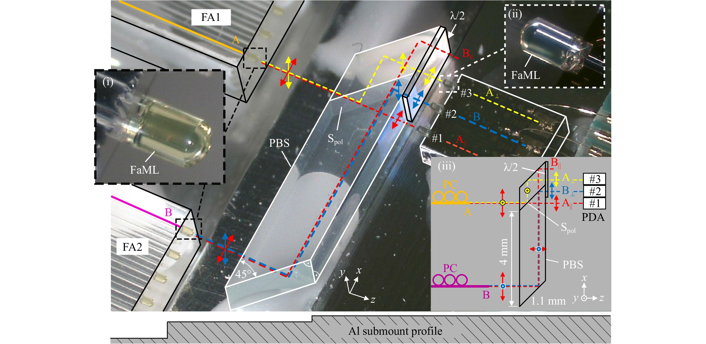
Fig. 7 Demonstration of an optical assembly using FaML, see Insets (i) and (ii) for a magnified view, including a discrete polarization beam splitter (PBS) in the collimated free-space beam path between a pair of FA and an optical chip with a PDA. The PBS consists of two right-angle glass prisms with a dielectric polarization-sensitive reflecting surface Spol in between. The beam paths are shown as colored dashed lines in the figure and in the top-view schematic shown in Inset (iii). The input fields at point A of FA1 and point B of FA2 are arbitrarily polarized, i.e., the linearly polarized constituents could have different amplitudes and phases. For coupling to a polarization-sensitive photonic integrated circuit (PIC), all output beams
${\color{khaki}{{ \rm A}}_{\color{khaki}\bot}}$ ,${\color{red}{{\rm A}_ {\|}}}\, $ , and${\color{blue}{{\rm B}_ {\bot}}} $ (beam${\color{red}{{\rm B}_ {\|}}} $ is lost) should be identically polarized. To this end, a half-wave plate (λ/2) is used to rotate the “vertical” linear polarization (blue, yellow) into the orientation of the “horizontal” linear polarization. Such an assembly could be used as a dual-polarization coherent receiver with the signal supplied by FA1 and the local oscillator by FA2, when replacing the rather simple PDA by a chip carrying a pair of 90° optical hybrids, each followed by a pair of balanced photodiodes. For measuring the coupling loss of each beam path, we subsequently feed the assembly with optical power through the FA1 and FA2 and maximize the photocurrents of PD#1, #2, #3 using fiber-based polarization controllers (PC). The resulting photocurrents are again compared to those obtained by directly feeding horizontally polarized light to the PDA chip via butt-coupled SMF. The losses are calculated according to the procedure described in the context of Table 2. We find an excess loss compared to butt coupling of 0.95 dB for path A–PD#1 (red), 1.44 dB for path A–PD#3 (yellow), and 2.18 dB for path B–PD#2 (blue). For the assembly, we first glue the PDA chip to the aluminum submount, followed by passive alignment and gluing of the PBS. The stepped profile of the aluminum submount is illustrated in the cross-sectional view at the bottom of the figure. In a second step, we align each FA passively with respect to the PDA chip and we again compare our passive alignment to an active alignment. Contrary to the previous demonstration without PBS, see Fig. 6, we now find a significant lateral (x-axis) offset between passive and active alignment positioning of the FA. Most prominently, the optimum entry points of paths A–PD#1 and A–PD#3 differ by 9 µm. We attribute these deviations to the manufacturing tolerances of the PBS, which are specified with ±25 µm for all length dimensions and ±0.2° for all cut angles, and which are significantly larger than the 2 µm translational and sub-0.1° rotational deviations that we have estimated for our FaML-assisted assembly process in the context of Fig. 6.To this end, we subsequently feed the assembly with optical power through FA1 and FA2 and subsequently maximize the photocurrents of PD#1, #2, #3 using fiber-based polarization controllers (PC). The resulting photocurrents are again compared to those obtained by directly feeding horizontally polarized light to the PDA chip via butt-coupled SMF. The losses are calculated using the procedure described in the context of Table 2. We find an excess loss compared to butt coupling of 0.95 dB for coupling from FA1 to PD#1 (path A–PD#1, red), of 1.44 dB for coupling from FA1 to PD#3 (path A–PD#3, yellow), and of 2.18 dB for coupling from FA2 to PD#2 (path B–PD#2, blue). The free-space beam in the connection B–PD#2 has an optical path length of 8.3 mm, which is 5 mm longer than the free-space path in connection A–PD#1. However, because we wanted to use one single lens design for all paths, the longer optical path length widens the beam and leads to higher losses. A free-space coupling distance of 3.3 mm would have been optimum.
For the assembly, we first glue the PDA chip to the aluminum submount, see Fig. 7, followed by passive alignment and gluing of the PBS. In a second step, we align FA1 and FA2 passively with respect to the PDA chip and again compare our passive alignment to an active alignment. This time, we find considerable lateral (x-axis) offsets between passive and active alignment of the FA. Most prominently, the optimum positions of FA1 for paths A–PD#1 and A–PD#3 differ by 9 µm. For our proof-of-principle demonstration, we therefore manually fix FA1 in the middle between the optimized positions for PD#1 and PD#3.
These deviations between passive and active alignment are in sharp contrast to our results from the assembly experiments without PBS, see Fig. 6. In those experiments, the free-space path length was also 3.3 mm as in the connection A–PD#1, but the optimum position of the FA could directly be found by passive alignment techniques, relying on machine vision only. We attribute the deviations in the experiment shown in Fig. 7 to the manufacturing tolerances of the PBS, which are specified to ±25 µm for all length dimensions and ±0.2° for all cut angles. This is significantly worse than the 2 µm translational and sub-0.1° rotational deviations that we have estimated for our FaML-assisted assembly process in the context of Fig. 6. This demonstrates that the level of precision that can be achieved with FaML-based optical microsystems is on par with or even exceeds the accuracy levels offered by standard discrete micro-optical components.
-
Finally, in our third set of experiments, we consider FaML assemblies printed to angled chip facets, see Inset (i) of Fig. 1, which are commonly used for semiconductor lasers and amplifiers, where unwanted back-reflections need to be effectively suppressed. In our experiments, we couple an InAlGaAs-based discrete-mode26 distributed-feedback (DFB) laser array to a single-mode fiber array (FA) using dedicated FaML both on the active chip and the fiber side. Fig. 8a shows a single connection of the assembly. The FaML are specifically designed to produce a non-planar beam path between the two facets, that contains only tilted or strongly curved optical surfaces S1, S2, S3, and S4, thereby greatly reducing back-reflections into the DFB chip. Note that the non-planar beam path is designed such that the top-view projection of the free-space section between the FaML is perpendicular to the chip and the FA edge, see Fig. 8b. This greatly simplifies alignment of the devices in assembly processes that are based on top-view camera vision in combination with linear translation parallel to the chip edges.
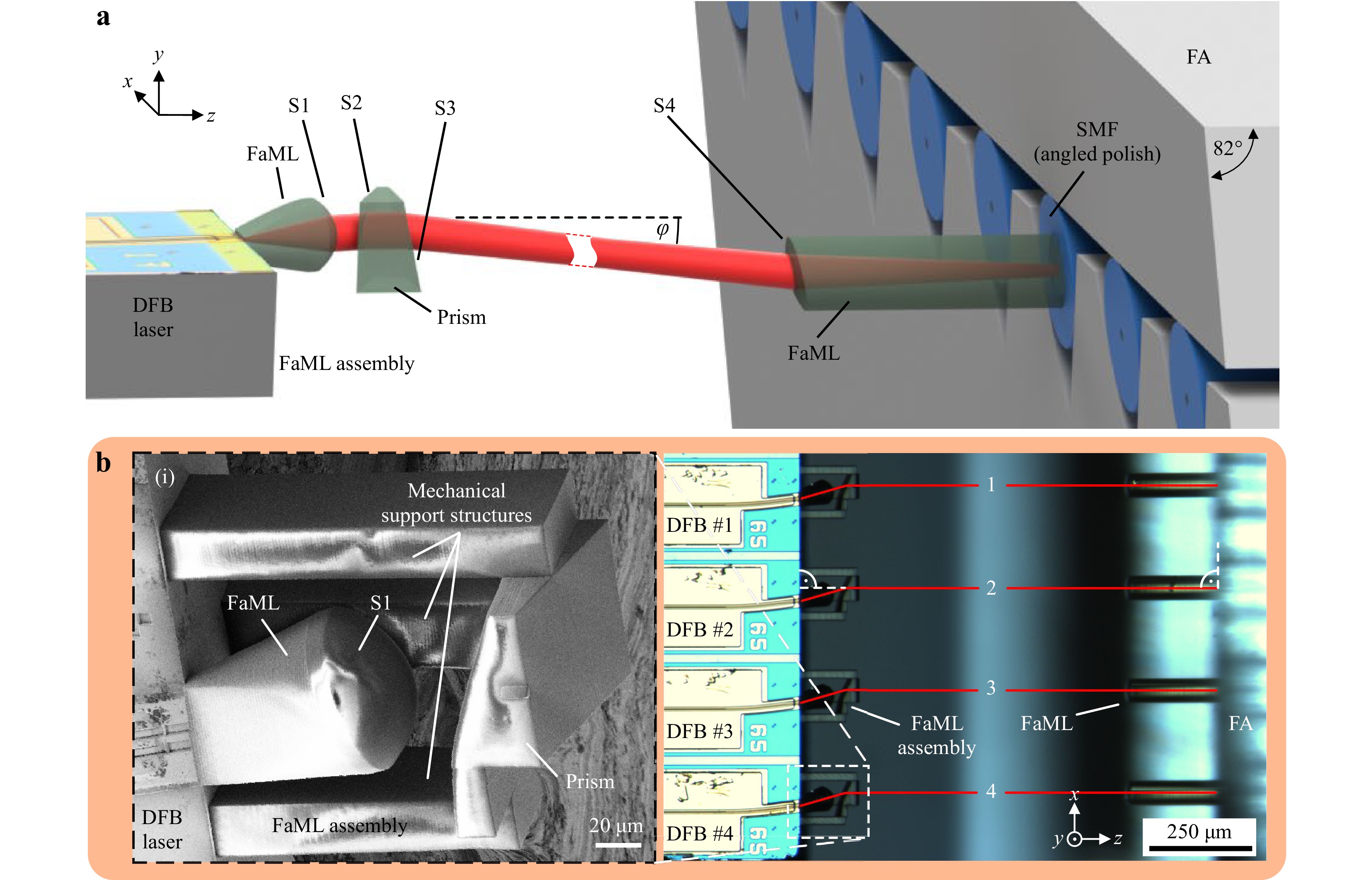
Fig. 8 Demonstration of an assembly consisting of an angled DFB laser array coupled to a single-mode fiber array (FA) through dedicated FaML both on the laser and the fiber facets. a Artist’s view of a single connection of the assembly. The FaML are designed to produce a non-planar beam path between the two facets that contains only tilted or strongly curved optical surfaces S1, S2, S3, and S4 and thereby avoids unwanted back-reflection into the laser. On the DFB side (left), a combination of a free-form lens and a prism expands, collimates, and redirects the beam. Mechanical support structures are omitted for better visibility. The strongly curved lens surface S1 collimates the beam to a diameter of 25 µm. The beam is then bent to the right with respect to the beam propagation direction by the first prism surface S2. Inside the prism, the light propagates parallel to the surface-normal of the DFB facet (z-axis). The second prism surface S3 then deflects the beam downwards in the (y, z)-plane by φ = 7° with respect to the z-axis. The FA features an end-face, which is polished at an angle of 8° from the (x, y)-plane, and which is equipped with a corresponding 3D-printed off-axis free-form lens (lens surface S4) that receives the beam. This arrangement shows minimal back-reflections and a coupling loss of about 2 dB, see Table 3. b Top-view image of the assembly. An array of four angled InP lasers is coupled to four fibers of an FA. Inset (i) shows an SEM picture of the FaML assembly on the laser side including mechanical support structures that hold the prism in place
The laser and fiber arrays used in the experiment feature a pitch of 250 µm. At the DFB side, a combination of a free-form lens and a prism expands, collimates, and redirects the beam. The strongly curved lens surface S1 collimates the beam to a diameter of 25 µm. The beam is then bent to the right with respect to the propagation direction by the first prism surface S2. Inside the prism, the light propagates parallel to the surface-normal of the DFB facet (z-axis). The second prism surface S3 then deflects the beam downwards in the (y, z)-plane by
$\varphi = 7{\text{° }}$ with respect to the z-axis, Fig. 8a. The FA features an end-face, which is polished at an angle of 8° from the (x, y)-plane and which is equipped with a corresponding 3D-printed off-axis free-form lens that receives the beam.For proper evaluation of the coupling efficiency in the assembly process, we first measured the laser output power vs. the injection current (P-I-curve) of each DFB laser prior to printing the FaML, see blue curve Fig. 9a. We then fabricate the FaML and actively align the FA to the DFB chip. In this step, the DFB chip is fixed in place, while the FA is positioned such that the light of DFB#1 and #4 is optimally coupled to the respective fiber, see Fig. 8b for the corresponding numbering. We again measure the P-I-curve of each laser through the fibers, see black trace in Fig. 9a for DFB#4. In a next step, we fix the FA with an UV glue, see Materials and Methods, and measure the P-I-curves again, see red trace in Fig. 9a for DFB#4. Comparing the P-I-curves before and after assembly, we find identical threshold currents and no indication of mode-hopping. Table 3 indicates the measured coupling losses before and after gluing the FA for all four DFB. Prior to gluing the FA, the coupling losses are very consistent with an average of 1.92 dB. For DFB#4, this value remains essentially unchanged after gluing the FA, whereas a small deviation is visible for DFB#1…3. This is attributed to the fact that the glue used for fixing the FA in our experiment was slightly thicker than designed. Specifically, the experiment relied on a milled aluminum submount containing a step to account for the different thicknesses of the DFB chip and the FA. This step came out slightly larger than designed, which had to be compensated by an approximately 400 µm-thick layer of glue, which is subject to shrinkage during the curing process. More precise fabrication of the submount step-height should alleviate this problem, see description of our first set of experiments in Section “Facet-attached microlens on an SiP chip” above. Still, the average loss per FaML pair amounts to 2.28 dB only, which is only 0.36 dB higher than the losses found for optimum alignment, see Table 3. We also investigated the relative loss for a translational lateral and for a rotational misalignment with respect to the optimum position prior to gluing the FA, see Fig. 9b, c, respectively. We find a slight deviation from an ideal rotationally symmetric characteristic, while the tolerances are similar to the ones observed in our first set of experiments in Section “Facet-attached microlens on an SiP chip” above.
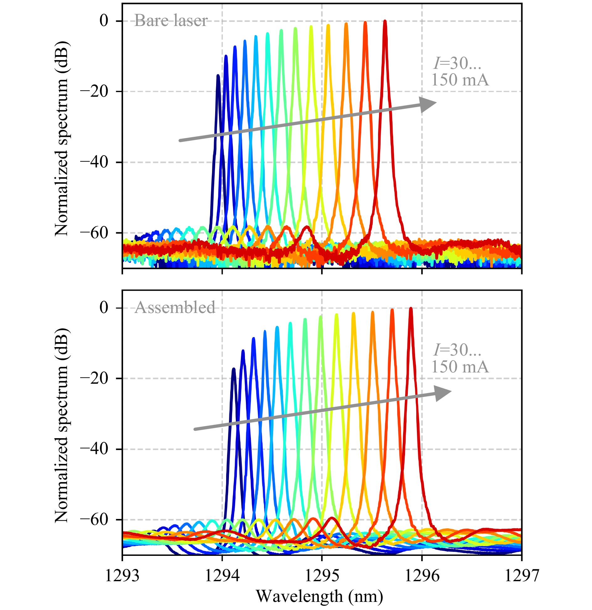
Fig. 9 Comparison of current-dependent emission spectra (resolution bandwidth 0.01 nm) of DFB#2 with and without the coupling arrangement shown in Fig. 8. For measuring the spectra of the bare laser, we pick up the light with a fiber placed deliberately at a large distance from the emitting facet (upper plot) to avoid back-reflections. The emission spectra remain essentially unchanged when packaging the device (lower plot) using the arrangement of Fig. 8. We only observe a small spectral shift, which we attribute to slight temperature differences. We conclude that our coupling scheme can reduce back-reflections to a level where they do not spoil the laser spectrum. The measurement and the influence of back-reflections is discussed in detail in Supplementary Section 4.
Laser number 1 2 3 4 avg. Loss per FaML pair
(actively aligned) [dB]1.9 1.9 2.0 1.9 1.92 Loss per FaML pair
(glued assembly) [dB]2.3 2.5 2.3 2.0 2.28 Table 3. Coupling losses for simultaneous coupling of a bar of 4 angled InP lasers to a fiber array.
We furthermore compare the spectra for one angled laser with and without the coupling arrangement of Fig. 8. For the spectra of the bare laser as a function of the operating current, see upper plot in Fig. 10, we pick up the light with a fiber placed deliberately at large distance for avoiding back-reflections. For the measurement of the packaged laser, lower plot in Fig. 10, we use a dual stage fiber optic in-line isolator (approximately 60 dB isolation), since the input to the optical spectrum analyzer (OSA) uses a mating sleeve for an open-ended fiber FC/PC connector without angle-polish. The spectra of the packaged device remain essentially unchanged, besides a small spectral shift, which we attribute to the commonly rather high thermally induced frequency shifts of InP-based DFB lasers (22 GHz/K) in combination with the fact that the temperature of the submount was not stabilized. From the results shown in Fig. 10, we conclude that the back-reflections of our FaML assembly do not spoil the laser spectrum, even for highly sensitive DFB devices. In our experiments, we also observed that leaving out the fiber-optic in-line isolator in the connection to the OSA lead to significantly broadened and distorted spectra due to reflections from the open fiber end. We further investigate the influence of back-reflections by conducting a separate experiment, in which we replace the isolator by a variable optical attenuator with angled physical contact (APC) connectors, see Supplementary Section 4. From this experiment, we estimate the spurious back-reflections from our FaML to be below −44 dB, see Supplementary Section 4 for details. The estimated amount of back-reflections is comparable to the levels achieved via advanced lensed fibers with anti-reflection (AR) coating27.
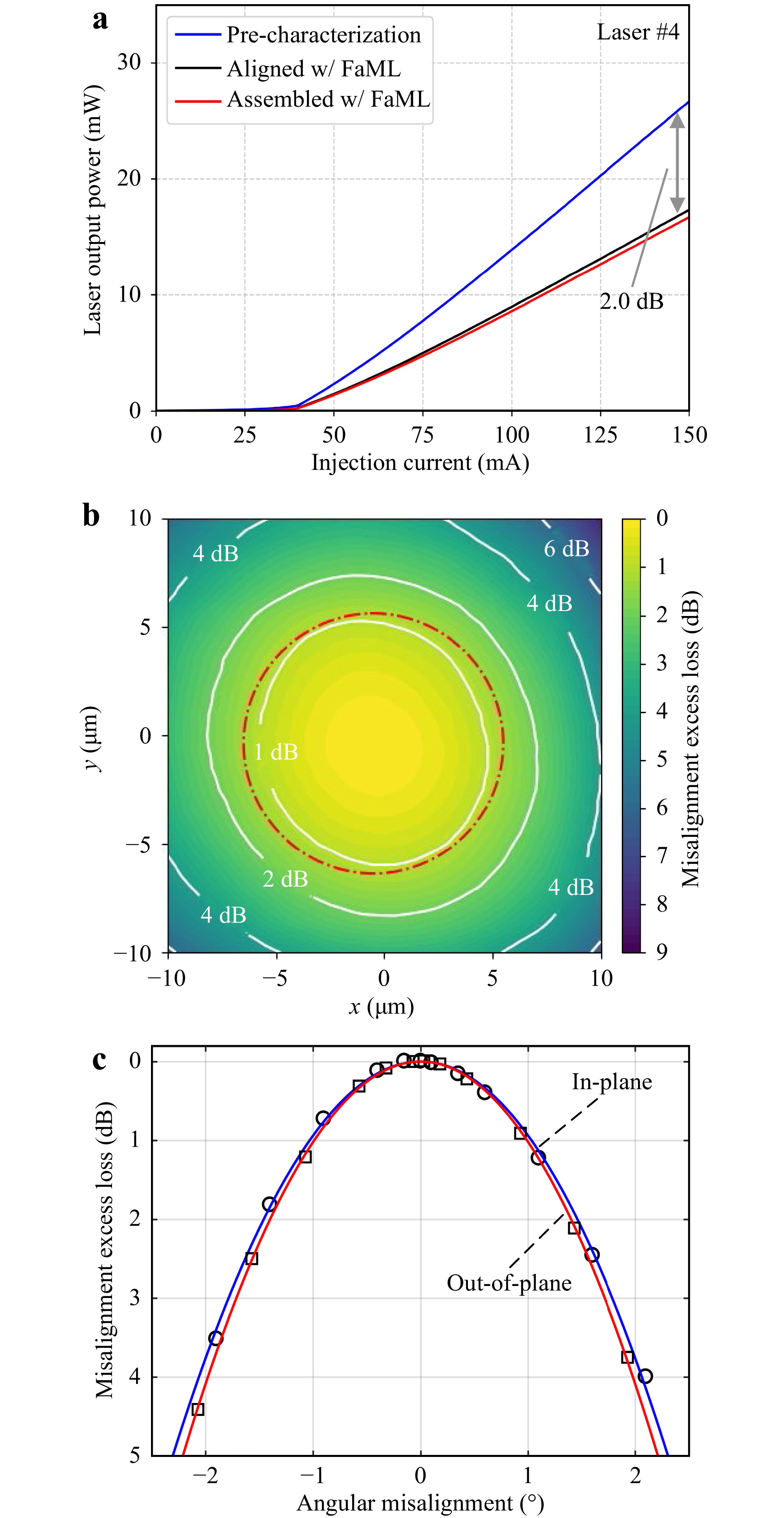
Fig. 10 Coupling losses and alignment tolerances for the laser-to-SMF assembly with angled facets, see Fig. 8. a Laser output power vs. injection current (P-I-curves) for the bare DFB#4 measured using an integrating sphere (pre-charaterization, blue), for the actively aligned device after printing the FaML and before applying the UV glue (aligned w/ FaML, black), and after glueing (assembled w/ FaML, red). The threshold current remains unchanged, and we find an assembly loss of 2.0 dB. b Excess loss for lateral misalignment in the (x, y)-plane of Fig. 8. The red dash-dotted circle indicates the expected radial 1 dB tolerance for a Gaussian beam with a MFD of 25 µm, see Supplementary Section 2.5. c Excess loss for rotational misalignment both in the substrate plane (circles, in-plane) and vertically to the substrate plane (squares, out-of-plane). The solid lines indicate Gaussian fits, which yield a waist diameter of 27.4 µm and 26.3 µm in the vertical and the horizontal directions. These values are reasonably close to their designed counterparts of 25 µm.
-
3D-printed facet-attached microlenses open a path towards efficient assembly of advanced photonic systems that may combine chip-based photonic integrated circuits (PIC) with free-space micro-optical elements. The concept offers an attractive alternative to currently used approaches for optical chip-chip and fiber-chip connections that mainly rely on grating couplers (GC) or edge couplers (EC). Grating couplers are mainly used in high index-contrast integration platforms such as SiP and suffer from strong polarization sensitivity28 and narrow spectral bandwidth29. Moreover, sophisticated designs such as bottom reflectors30 are required to achieve low insertion loss, and package geometries with “out-of-plane” fibers connected to the top of the chip are often unfavorable. Using EC, it is possible to achieve very low insertion loss, large spectral bandwidth, and low sensitivity to polarization31. However, EC require very tight alignment tolerances, often on the sub-micrometer level such that active alignment is unavoidable. This leads to technically complex assembly processes, in particular when simultaneous coupling of multiple channels is required. Specifically, active alignment necessarily requires an optical test signal to be generated during the assembly process, which is often associated with operating parts of the optical system via suitable electrical probes, thus further complicating the workflow. Moreover, tight lateral tolerances render assembly processes particularly sensitive with respect mechanical misalignment by practically unavoidable shrinkage of glue during curing. In addition, proper matching of mode fields may represent a challenge, especially when connecting waveguides with vastly different refractive-index-contrasts. Recently, a highly scalable passive edge-coupling approach was demonstrated, which couples light from a ribbon fiber to a SiP chip using metamaterial suspended-membrane tapers32,33 and etched V-grooves, offering insertion losses of 0.9…1.5 dB. However, additional process steps are required for the metamaterial under-etch, which are not generally available. Furthermore, the proposed method requires tapers of around 1 mm and V-grooves of around 300 µm length, thereby consuming precious design space on the PIC. Photonic wirebonding34,35 represents another alternative that circumvents the need for active alignment. However, the method is only suited for bridging comparatively short distances (typically < 400 µm) between devices and requires good accessibility of the facets upon fixing the chips, thereby restricting the design freedom for the assembly architectures.
Our work demonstrates that FaML can overcome these problems, enabling low-loss edge coupling with relaxed alignment tolerances over mm-scale distances. These prospects were partly mentioned as a theoretical possibility in our earlier publication20, however without proving the practical feasibility under real technical constraints related, e.g., to limited angular and translational alignment accuracy of assembly machines, to shrinkage of glues during curing, or to fabrication inaccuracies of the FaML, which may lead to pointing errors of the emitted beams. The work presented here provides this proof and additionally covers highly relevant use cases for FaML, comprising pluggable fiber-chip connections, coupling with ultra-low reflection based on angled interfaces, as well as free-space coupling over large distances with intermediate micro-optical elements. On a quantitative level, we demonstrate low-loss FaML-based coupling interfaces for edge emitting SiP chips, featuring insertion losses of 1.4 dB per interface along with transverse 1 dB-alignment tolerances of ±6 µm. This corresponds to the lowest loss so far obtained for edge-emitting silicon photonic waveguide interface with micrometer-scale alignment tolerances. The results are highly reproducible, which is confirmed by the low variances of the losses obtained in our array coupling experiments, see Tables 1-3. The high degree of reproducibility is a direct consequence of the relaxed alignment tolerances – we quantify this aspect and support it by Monte Carlo simulations in Supplementary Section 2.9. For properly designed FaML, the accuracy of the machine used in our experiments should, in most cases, not lead to any measurable excess loss due to passive alignment.
The relaxed alignment tolerances open a path towards passive assembly techniques exploiting machine vision and/or simple mechanical stops and even permit re-pluggable fiber-to-chip connectors based on mass-producible injection-molded plastic parts. In comparison to the aforementioned metamaterial-based suspended-membrane tapers32,33, our method provides similar coupling performance while being much more flexible. Facet-attached microlenses are compatible with all photonic integration platforms and can be applied to vastly different multi-chip and fiber-chip assemblies – without any need for technologically demanding under-etching at the chip facet. Our approach further allows to insert discrete micro-optical components into the collimated beams between chip-based PIC, and the design of FaML based micro-optical coupling elements can be easily adapted for angled facets with low-back-reflection. We further believe that our approach is highly scalable from a fabrication point of view. Printing on facets of FA and cleaved bars of InP devices can be efficiently accomplished by working with device stacks that can be processed from the surface-normal direction of the facets. In case of chips with deep-etched optical facets, FaML can be printed on a wafer level from a direction normal to the wafer surface, see Materials and Methods. With respect to fabrication throughput, the writing time for the FaML is clearly an important aspect and probably the main scalability bottleneck of today’s lithography systems. In general, the writing time of a given FaML depends on many parameters such as the volume, the required printing resolution, as well as the size, the curvature, and the required quality of the optically relevant surfaces. While small lenses typically require writing times of the order of a minute, the writing times for bigger lenses as needed for large beam diameters can currently still exceed ten minutes. In the future, these writing times may be reduced by orders of magnitude, using, e.g., novel multi-photon printing techniques such as light-sheet 3D microprinting36 or projection printing with spatio-temporal focusing37, rendering the FaML-approach even more attractive. Exploiting fully automated direct-write 3D laser lithography might hence open a path towards highly scalable and robust assembly processes of advanced photonic integrated systems.
-
We demonstrate the potential of 3D-printed facet-attached microlenses (FaML) for advanced photonic system assembly. FaML can be printed with high precision to the facets of optical components using multi-photon lithography, thereby offering the possibility to shape the emitted beams by freely designed refractive surfaces. The beams can be collimated to comparatively large diameters that are independent of the device-specific mode fields, thereby relaxing both axial and lateral alignment tolerances. This renders costly active alignment obsolete and opens the possibility to insert discrete optical elements such as optical isolators into the free-space beam paths between PIC facets. We show the viability and the versatility of the concept in a series of selected demonstrations. In a first set of experiments, we couple fiber arrays (FA) to arrays of edge-coupled silicon photonic (SiP) chips, reaching insertion losses of 1.4 dB per interface with a translational lateral 1 dB alignment tolerance of ±6 µm and a rotational 1 dB alignment tolerance of 1.1°. To the best of our knowledge, this is the lowest loss so far demonstrated for an edge-emitting SiP waveguide interface with micron-scale alignment tolerances. We also show that the outstanding alignment tolerance of our scheme allows for reproducible coupling using a simple LEGO brick for detachable mechanical connection. In a second set of experiments, we further demonstrate free-space transmission over distances in the millimeter-range, using standard machine-vision techniques for alignment of the respective devices. In this experiment, we insert a discrete micro-optical polarization beam splitter prism into the beam path between a single-mode fiber (SMF) array and array of edge-coupled indium-phosphide (InP) photodetectors. A third set of experiments is dedicated to interfaces between angled DFB lasers and SMF arrays. In this context, we demonstrate coupling with ultra-low back-reflection by connecting planar devices through non-planar beam paths that only comprise tilted optical surfaces. We achieve coupling losses of approximately 2 dB and estimate −44 dB of spurious back-reflection. Based on these exemplary demonstrations of the outstanding versatility of the FaML concept, we believe that the approach opens an attractive path towards advanced photonic system assembly that may overcome most of the current limitations.
-
Silicon photonic (SiP) chips: The SiP chips used in our experiments were fabricated at IMEC, Belgium, using the ISIPP50G platform. The test chips contain edge couplers (EC) with so-called inverse tapers, which are arranged in a loopback-configuration with a pitch of 127 µm, see Fig. 2. By observation with an IR microscope objective (Olympus LMPlan IR 100x/0.80) with a numerical aperture (NA) of 0.8, the mode-field diameter (MFD) was measured to be 2.5 µm at the chip facet. For calculating coupling losses, we assume a waveguide loss of 0.17 dB/mm and 0.08 dB/mm for TE and TM-polarization, respectively. For the Loopbacks (1, 8) and (2, 7), see Fig. 2, we further account for a loss of 0.3 dB per waveguide crossing. The polarization-dependent loss (PDL) of the EC amounts to 0.5 dB. These numbers are specified by IMEC’s Process Design Kit (PDK).
Multi-photon lithography: The 3D-printed microlenses were fabricated from negative-tone photoresist (VanCore A, Vanguard Automation GmbH, Karlsruhe, Germany; refractive index n = 1.53 at 1550 nm) using an in-house-built lithography system with a 63x/1.4 objective (Zeiss Plan-Apochromat 63x/1.4 Oil DIC M27), galvanometer-actuated mirrors, and a 780 nm femtosecond laser (Menlo C-Fiber 780 HP, pulse width 58 fs). We use automated procedures for detection of the height and tilt of chips and FA. For the SiP chips, we reach a lateral and vertical alignment precision35 of the order of 100 nm. Further information on the resist material and on the stability of printed FaML structures is given in Supplementary Section 6.
Lenses are printed to the fiber arrays (FA) with the axis of the lithography beam perpendicular to the fiber facets, while the fiber cores are back-illuminated for easier detection. Similarly, the lenses on the InP components are printed “from the front”, with the axis of the lithography laser beam perpendicular to the chip facets, and the geometry of the ridge waveguide structure is detected for position referencing. In contrast to this, we print the SiP lenses “from top” with the axis of the lithography perpendicular to the top surface of the chip. This allows for precise detection of marker structures on the chip surface and opens a path towards wafer-level printing of FaML to deep-etched device facets prior to chip separation. When printing to vertical device facets “from top”, the opaque chip edge blocks part of the lithography beam, thus reducing the power in the focus. This is compensated by using a position-depend dose adaptation close to the device facet.
Passive alignment and assembly process: For passive alignment and assembly we use a custom assembly machine (ficonTEC Service GmbH) that relies on industry-standard machine vision techniques, see Supplementary Section 3 for details. The alignment is based on data from a top-view and a bottom-view camera, as well as on high-precision distance measurements using a sensor that exploits a chromatic confocal measurement principle38. To aid the detection of fiber arrays, we use 3D-printed markers, see Inset (i) of Fig. 6a and Supplementary Section 3 for details. Once aligned, the components are fixed in place using UV glue (Optocast 3410 Gen 2, EMI Inc.). This glue contains silica filling material and features low shrinkage to permit gluing gaps of variable widths up to at least 200 µm without notable displacement of the devices during curing.
Microlens simulation: For the numerical optimization of microlens surfaces, we use an in-house simulation software written in Python and running on a graphic processing unit (GPU). The software relies on the scalar wide-angle unidirectional wave-propagation method proposed in Ref39. This allows for fast and reliable wave-optical modeling of micro-optical components beyond the thin-element approximation and for wave-optical assessment of alignment and fabrication tolerances both in the lithography and the assembly processes. Various simulated field plots are found in Supplementary Fig. S9.
-
This work was supported by the Deutsche Forschungsgemeinschaft (DFG, German Research Foundation) under Germany’s Excellence Strategy via the Excellence Cluster 3D Matter Made to Order (EXC-2082/1-390761711) and the Collaborative Research Center WavePhenomena (CRC 1173), by the Bundesministerium für Bildung und Forschung (BMBF) via the projects PRIMA (# 13N14630), DiFeMiS (# 16ES0948), which is part of the programme “Forschungslabore Mikroelektronik Deutschland (ForLab), and Open6GHub (# 16KISK010), by the European Research Council (ERC Consolidator Grant ‘TeraSHAPE’; # 773248), by the H2020 Photonic Packaging Pilot Line PIXAPP (# 731954), by the Alfried Krupp von Bohlen und Halbach Foundation, and by the Karlsruhe School of Optics and Photonics (KSOP).
3D-printed facet-attached microlenses for advanced photonic system assembly
-
Yilin Xu1, 2, *, ,
 ,
, - Pascal Maier1, 2,
- Mareike Trappen1, 2,
- Philipp-Immanuel Dietrich1, 2, 3,
- Matthias Blaicher1, 2,
- Rokas Jutas1,
- Achim Weber3, 4,
- Torben Kind4,
- Colin Dankwart4,
- Jens Stephan5,
- Andreas Steffan5,
- Amin Abbasi6,
- Padraic Morrissey7,
- Kamil Gradkowski7,
- Brian Kelly8,
- Peter O’Brien7,
- Wolfgang Freude1,
-
Christian Koos1, 2, 3, *, ,
- Light: Advanced Manufacturing 4, Article number: 3 (2023)
- Received: 29 July 2022
- Revised: 06 January 2023
- Accepted: 10 January 2023 Published online: 17 April 2023
doi: https://doi.org/10.37188/lam.2023.003
Abstract: Wafer-level mass production of photonic integrated circuits (PIC) has become a technological mainstay in the field of optics and photonics, enabling many novel and disrupting a wide range of existing applications. However, scalable photonic packaging and system assembly still represents a major challenge that often hinders commercial adoption of PIC-based solutions. Specifically, chip-to-chip and fiber-to-chip connections often rely on so-called active alignment techniques, where the coupling efficiency is continuously measured and optimized during the assembly process. This unavoidably leads to technically complex assembly processes and high cost, thereby eliminating most of the inherent scalability advantages of PIC-based solutions. In this paper, we demonstrate that 3D-printed facet-attached microlenses (FaML) can overcome this problem by opening an attractive path towards highly scalable photonic system assembly, relying entirely on passive assembly techniques based on industry-standard machine vision and/or simple mechanical stops. FaML can be printed with high precision to the facets of optical components using multi-photon lithography, thereby offering the possibility to shape the emitted beams by freely designed refractive or reflective surfaces. Specifically, the emitted beams can be collimated to a comparatively large diameter that is independent of the device-specific mode fields, thereby relaxing both axial and lateral alignment tolerances. Moreover, the FaML concept allows to insert discrete optical elements such as optical isolators into the free-space beam paths between PIC facets. We show the viability and the versatility of the scheme in a series of selected experiments of high technical relevance, comprising pluggable fiber-chip interfaces, the combination of PIC with discrete micro-optical elements such as polarization beam splitters, as well as coupling with ultra-low back-reflection based on non-planar beam paths that only comprise tilted optical surfaces. Based on our results, we believe that the FaML concept opens an attractive path towards novel PIC-based system architectures that combine the distinct advantages of different photonic integration platforms.
Research Summary
Multi-photon lithography: 3D-Printed microlenses enable scalable photonic system assembly
3D-printed facet-attached microlenses (FaML) can improve the scalability of the assembly of photonic integrated circuits (PIC). Currently, the assembly of PIC relies on complex and expensive active alignment techniques. FaML can be printed onto the facets of optical components using multi-photon lithography, offering the possibility to collimate the emitted beams to a comparatively large diameter that is independent of the specific device, thereby relaxing both axial and lateral alignment tolerances. The FaML concept allows for passive assembly using industry-standard machine vision or simple mechanical stops. Experiments show the versatility of the concept in creating pluggable fiber-chip interfaces, in combining PIC with discrete micro-optical elements, and in coupling light with ultra-low back-reflection. Based on these results, the authors believe that FaML may offer an attractive path towards novel PIC-based system architectures.


Rights and permissions
Open Access This article is licensed under a Creative Commons Attribution 4.0 International License, which permits use, sharing, adaptation, distribution and reproduction in any medium or format, as long as you give appropriate credit to the original author(s) and the source, provide a link to the Creative Commons license, and indicate if changes were made. The images or other third party material in this article are included in the article′s Creative Commons license, unless indicated otherwise in a credit line to the material. If material is not included in the article′s Creative Commons license and your intended use is not permitted by statutory regulation or exceeds the permitted use, you will need to obtain permission directly from the copyright holder. To view a copy of this license, visit http://creativecommons.org/licenses/by/4.0/.

 DownLoad: