


-
Micrometre-scale light-emitting diode (micro-LED)1-8 displays have attracted significant interest owing to their exciting features, such as high brightness and contrast ratio, low power consumption, and prolonged lifetime9-11. In 2021, Ji et al. comprehensively summarised the progress and future challenges of micro-LED displays and considered them as next-generation displays8. Nevertheless, some technical bottlenecks remain that should be resolved for the further advancement of this technology for mass production. In addition to the mass-transfer challenge, significant differences in electroluminescence (EL) efficiencies and the threshold voltages of red, green, and blue (RGB) LEDs12 inevitably complicate the driving circuit design of display panels. Furthermore, blue LEDs exhibit relatively better stability characteristics than their red and green counterparts, which can result in a high risk of colour shift after long-term usage. Therefore, alternative strategies should be explored to harness the full potential of micro-LED technology for high-performance full-colour displays. Therefore, blue micro-LEDs integrated with red and green colour conversion materials (CCMs) have recently emerged as an effective method of developing efficient full-colour displays4. RGB emissions can be attained by combining phosphors or quantum dots (QDs) with ultraviolet (UV) or blue LEDs13-19. In 2022, Triana et al. comprehensively summarised the progress of luminescent nanomaterials, including QDs, as efficient energy converters for advanced displays20. In addition to the fine patterning of QD films as colour conversion layers (CCLs)21-24 for efficient and complete photoconversion, another major bottleneck is the crosstalk effect among adjacent pixels because of the wide view-angle feature of LED chips15. In 2020, we successfully demonstrated a 4-inch full-colour prototype incorporating a bottom-emitting blue micro-LED backlight and QD CCLs25. The colour gamut of this display reached up to 129% of the National Television Standards Committee (NTSC). However, the tolerance of the fabrication process was rather small, because it was fabricated on a colourless polyimide substrate with a thickness of 10 μm. Maintaining the vertical distance between the blue light emission and the CCLs at ≤10 μm is considerably difficult because certain deviations may occur during thin-film transistor (TFT) manufacturing, micro-LED bonding, or module assembly steps. Thus, there remains a high probability of the crosstalk effect under undemanding fabrication conditions.
In this study, we focused on conventional top-emitting structure and systematically simulated the factors that contribute to the crosstalk effect and observed that filling the space between each micro-LED chip with a light-blocking matrix (LBM) can be a promising solution to alleviate this risk. Based on the simulation results, a black LBM matrix was finely moulded on the top-emitting blue micro-LED backlight through a moulding and plasma etching technique. With the black LBM, the view-angle of the backlight was reduced by 40° and the crosstalk effect was efficiently suppressed. Eventually, a full-colour display was manufactured by integrating an LBM-moulded blue micro-LED backlight with red and green QD CCLs. The colour gamut of our display prototype can reach as high as 122% of the NTSC.
-
Because of the emanative emission of the inorganic micro-LED and QD layers, the crosstalk of the QD-LED display system significantly affects the colour purity and colour gamut. To determine potential solutions for alleviating the crosstalk risk in top-emitting colour-converted micro-LEDs (Fig. 1), we conducted a series of simulations. First, we performed a simulation of conventional top-emitting structures without an LBM (Fig. S1 in the Supplementary Information). In this model (Fig. S2a, Supplementary Information), three components, including the micro-LED pitch, black bank critical dimensions (CDs), and gaps (the vertical distance between the sapphire surface and CCLs), were considered the main factors contributing to the photoconversion performance. Based on this model, the crosstalk (XT%=Lsubpixel/Lmicro-LED, where Lsubpixel is the luminance of adjacent pixels and Lmicro-LED is the luminance of the lit blue micro-LED) was estimated by comparing the brightness difference of blue emissions between the lit micro-LED and adjacent sub-pixels. Severe crosstalk (XT%=19.9%) was observed in the 4-inch chip pixel design (Fig. S3, Supplementary Information), because the pitch was similar to that of the micro-LED chips. XT% was still as high as 16.01%, even after the gap was reduced to 0 μm. A lower crosstalk effect was observed when the micro-LED pitch was increased, and the XT% was 1.3% at a 450 μm pitch. Under this condition, both the gap and black bank CD factors had a limited influence on the crosstalk. The detailed simulation results for this model are provided in Table S1 (Supplementary Information). Nevertheless, such a high micro-LED pitch conflicts with the demand for high-resolution displays. Therefore, alternative techniques are crucial for mitigating the risk of the crosstalk effect without compromising display performance.
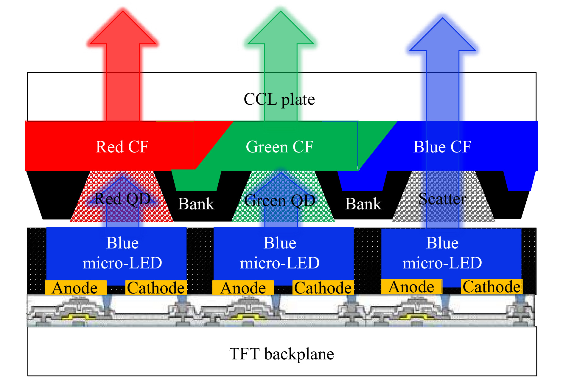
Fig. 1 Schematic architecture of the top-emitting colour-converted full-colour micro-LED display prototype.
Considering that crosstalk occurs among adjacent micro-LED chips, a potential solution could be to separate them by incorporating LBMs. To confirm our hypothesis, we designed another simulation model (Fig. S2b, Supplementary Information). In this model, in addition to the gap, two other factors, the transmittance and thickness of the LBM, were considered. As indicated in Table 1, the crosstalk decreased significantly when an LBM with absolute light-blocking ability and thickness equal to that of the micro-LEDs was employed. The colour gamut of the resulting prototype reached ~120% NTSC, even when the gap was maintained at approximately 20 μm. Considering the limited light-blocking ability of conventional capping materials, we simulated the crosstalk effect under different LBM transmittances. Under an equal LBM height to the micro-LED and with a 0 μm gap, the crosstalk was as low as 0.2%, and the colour gamut was higher than 126% NTSC when the transmittance of the LBM was less than 1% (Table S2, Supplementary Information). When the LBM height was increased by 10 μm compared with that of the micro-LED chips, no influence on the crosstalk was observed, whereas the emission brightness was reduced by 9%. These simulation results indicated that the crosstalk can be efficiently curbed by introducing an LBM matrix with a transmittance of <1% to the micro-LED backlights.
Gap Red Green Blue XT% Gamut (NTSC) 0 μm 


0 128.0% 10 μm 


0.22% 125.4% 15 μm 


0.57% 122.0% 20 μm 


1.3% 118.7% 25 μm 


2.0% 116.5% 30 μm 


3.6% 114.0% Table 1. Crosstalk simulation of photoconversion performance for the top-emitting model with the black LBM under different gaps between the blue backlight and CCL plate.
Based on the TFT backplane manufacturing, micro-LED transfer and bonding procedure described in our previous paper25, a 4-inch pristine blue micro-LED backlight was first fabricated. Nevertheless, it is not a simple task to effectively introduce an LBM into micrometre-scale spaces between adjacent micro-LEDs. Meanwhile, the side emissions among adjacent blue micro-LEDs should be completely blocked, whereas the forward emissions should be maintained. Therefore, we proposed three schemes: press-assisted moulding, inkjet printing (IJP), and metal stencil printing (MSP) (Fig. 2). Based on the corresponding LBM materials for these three approaches (semi-solid gel, liquid ink, and paste state), we conducted three experiments to introduce the LBM into micro-LED panels. As indicated in Fig. 2a, the LBM was completely moulded inside the micro-LED spaces using the first approach. However, a “U” shape film morphology (Fig. 2b) and rough patterns (Fig. 2c) were achieved through the IJP and MSP methods. In the following, we focus on the moulding method to fabricate the LBM on micro-LEDs. The “U” shape morphology can be attributed to the fluid dynamics of IJP inks, which made it difficult to realise square edges. For the rough patterns fabricated using the MSP method, the difficulties primarily fall on the design of suitable metal stencil patterns and the development of suitable black pastes. Designing a metal mask with completely blank rings surrounding micro-LED chips is impossible. Thus, we designed a mask with approximate rings, where the metal blocks corresponding to the micro-LED positions were connected using narrow metal stripes (Fig. S4, Supplementary Information). Based on this design and the fluid characteristics of the pastes, it was anticipated to encircle the micro-LED chips with black paste while failing. The following section focuses on the first approach.
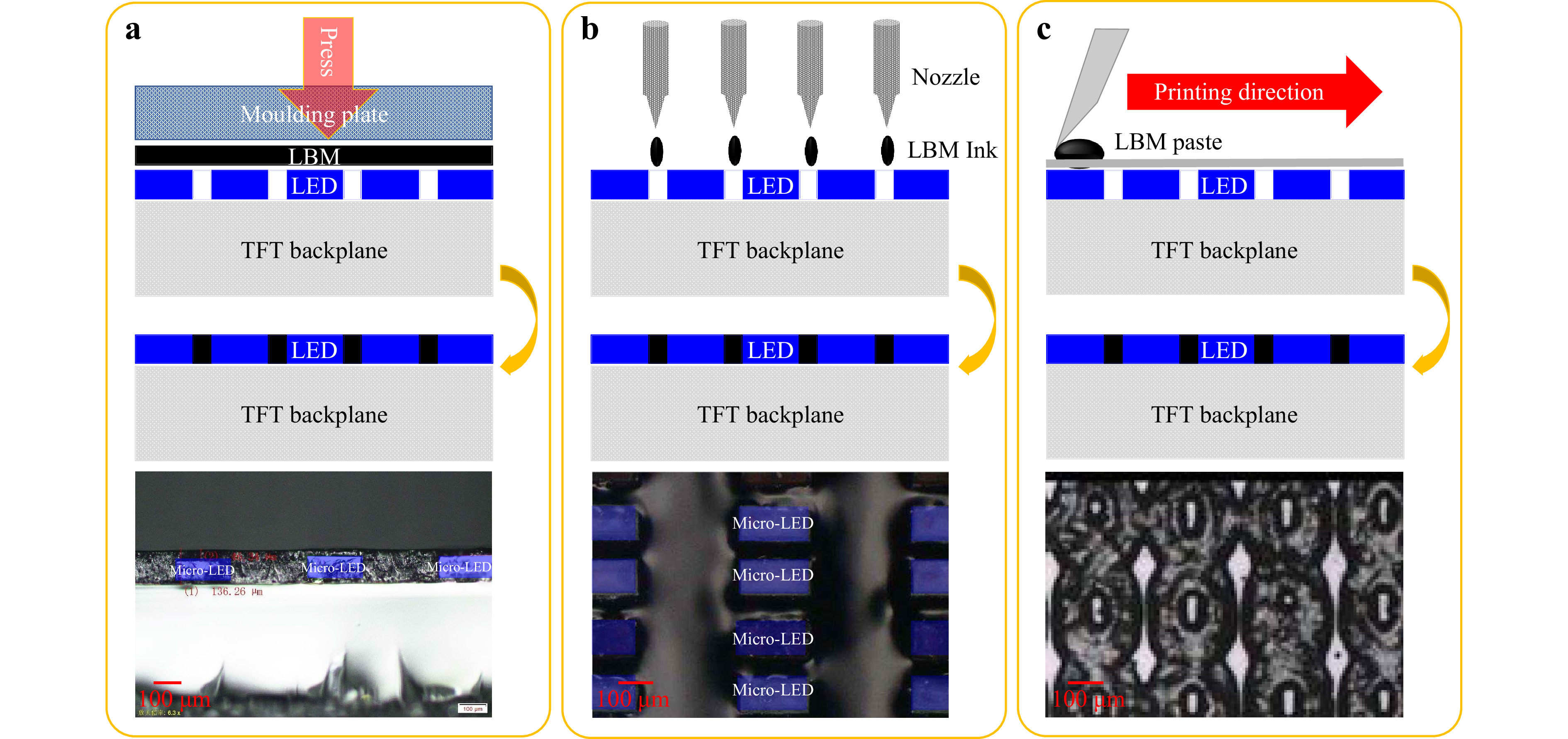
Fig. 2 Proposed schemes to fabricate LBM for the blue micro-LEDs backlight. Schematic process and corresponding LBM morphologies of a press-assisted molding, b IJP, and c metal stencil printing techniques.
Before fabricating the LBM matrix on a 4-inch pristine blue micro-LED backlight, the transmittance of the corresponding black LBM (thermosetting silica gel) was measured. As shown in Fig. S5a (Supplementary Information), when the film thickness was higher than 40 μm, the corresponding transmittance in the blue emission range was lower than 0.1%, which can also be verified in Fig. S5b (Supplementary Information). According to the aforementioned findings, the light-blocking ability fully satisfied the requirement for the LBM, considering that the space of adjacent micro-LEDs was wider than 50 μm. Based on the aforementioned black silica gel, an LBM matrix was moulded on top of the pristine backlight (Fig. S6a). As shown in Fig. S6b, the fabricated backlight displayed a high luminance uniformity along the full panel, indicating that the moulded LBM layer was very smooth. The crosstalk phenomenon (Fig. 3a, c) was successfully curtailed (Fig. 3b) with the aid of the LBM, and the panel view angle at half brightness maximum was also successfully reduced by almost 40° (Fig. 3d). However, the panel on-axis brightness decreased severely compared with the pristine state and remained at only ~2% of the initial value (Fig. 3e). This can be primarily attributed to the thick (>30 μm) LBM layer on the sapphire surface (Fig. S5c). Such severe brightness loss is not appropriate for further applications.
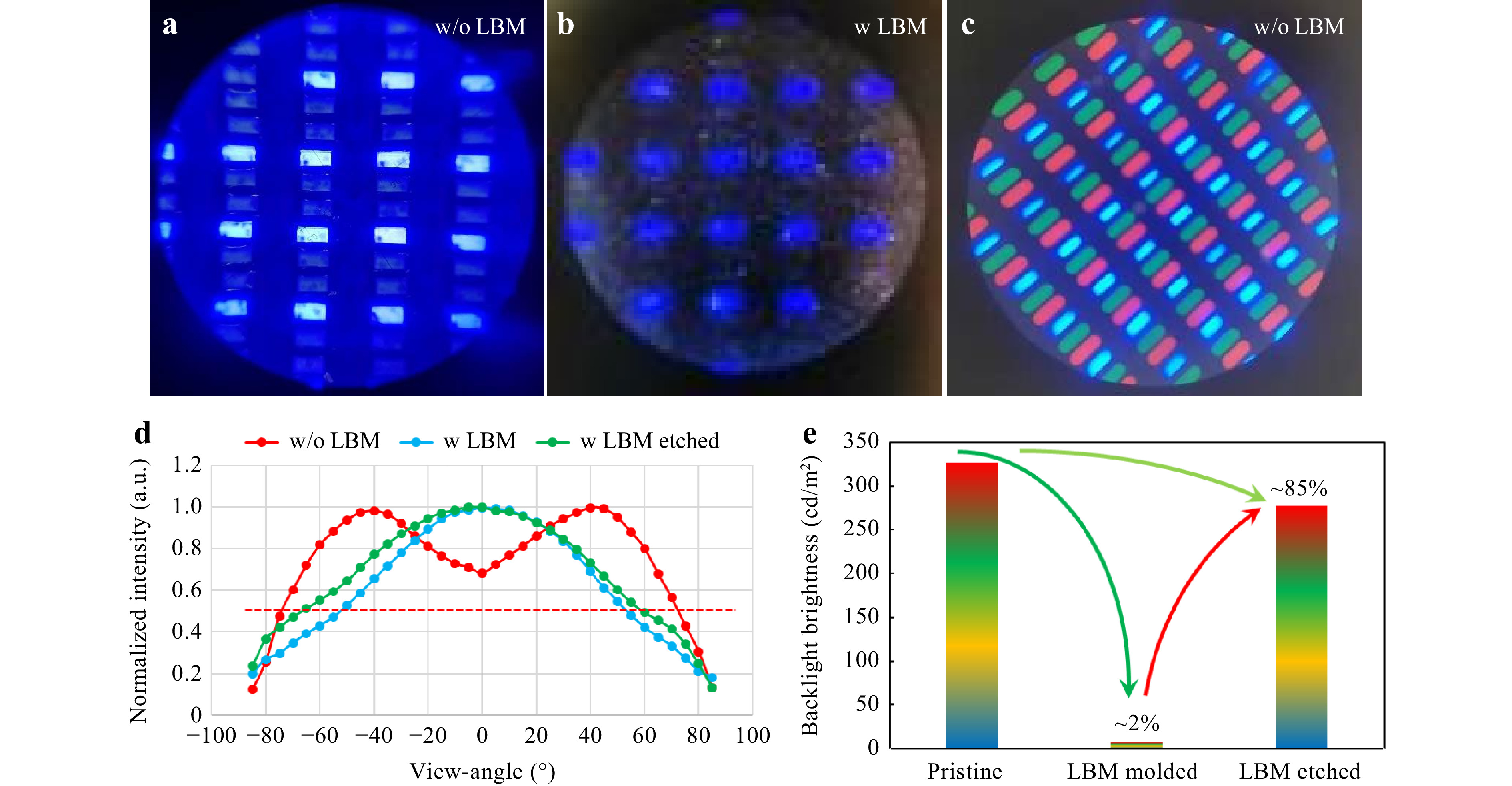
Fig. 3 Optical performance of the top-emitting active matrix blue micro-LEDs backlight. Pixel photograph of the panels a without and b with the LBM when only one micro-LED was lit. c Pixel photograph of the panel with the CCL plate directly stacked on top of blue micro-LED without an LBM when only one micro-LED was lit. d Brightness and e view-angle characteristics of backlights.
Therefore, we sought to explore a method of removing the remaining LBM to efficiently extract the trapped light. The plasma etching technique (Fig. S7, Supplementary Information) was used to lap the LBM layers. Tetrafluoromethane (CF4) and oxygen (O2) were adopted as gas sources, considering that the main constituents of the LBM were silica gel and other organic additives. As indicated in Fig. 4a, both of these gases were implemented as F* and O* sources, respectively, to remove the Si and C/H elements and thus lap the LBM layer. A suitable process recipe was used (microwave power: 4000 W, chamber pressure: 1.27 mTorr, CF4 flow: 500 cc/min, O2 flow: 2000 cc/min, and time: 15 min), a >20-μm-thick LBM test sample was lapped using this approach (Fig. 4b). Furthermore, the root-mean-square surface roughness of the lapped LBM was as low as 0.23 μm (Fig. 4c), which further suggested that plasma etching is suitable for reducing black silica gel. Finally, sapphire surfaces were observed (Fig. 4d) after the top LBM films were removed. As a result, approximately 83% of the on-axis light was successfully extracted without changing the view-angle characteristics (Fig. 3d, e).
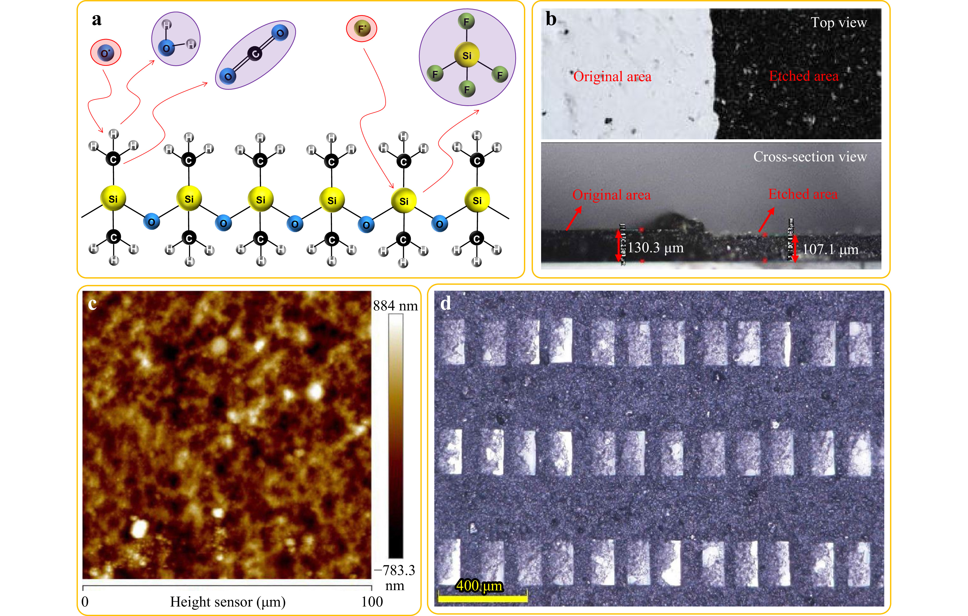
Fig. 4 Plasma etching and the resulting film morphology of the black LBM films. a Schematic illustration of the plasma etching process. b Top-view and cross-sectional microscopic and c atomic force microscopy images of the black LBM films under plasma etching treatment. d Microscopic images of the blue micro-LED backlight molded with the LBM after plasma etching treatment.
With a prefabricated top-emitting blue micro-LED backlight, a CCL plate was developed, and both of these components (i.e., micro-LED chip and CCL plate) were assembled together to develop a full-colour display (Fig. S8, Supplementary Information). Similar to our previous studies21, 23, 25, red and green CdSe QDs were selected as CCLs, and a UV-induced polymerisation method was employed to obtain micrometre-thick QD films for effective photoconversion. As shown in Fig. S9 (Supplementary Information), bright and vivid red and green emissions were achieved, indicating that the CCL patterns were precisely fabricated using the IJP approach. Finally, the blue top-emitting backlight and CCL plates were carefully assembled to obtain the target full-colour display prototype (Fig. 1).
Peking University logos illuminated in different colours using this developed display prototype are shown in Fig. 5d–f, revealing high colour purities (Fig. 5b). Furthermore, a colourful photo of a bus (Fig. 5a) was also created using our CCL-integrated micro-LED display (more display images are provided in the Supplementary Video). These results indicate that the integration of CdSe QD CCLs with top-emitting LEDs is an effective approach for manufacturing efficient full-colour micro-LED displays. The colour gamut of this prototype was also estimated, as shown in Fig. 5c (for detailed Commission Internationale de L’Eclairage (CIE) coordinates, please see Table S3), and could reach as high as 91% of Broadcasting Service Television 2020 (BT.2020) or 122% NTSC. This colour gamut performance was considerably higher than that of displays based on RGB micro-LED chips with 80.5% BT.2020 or 108% NTSC.
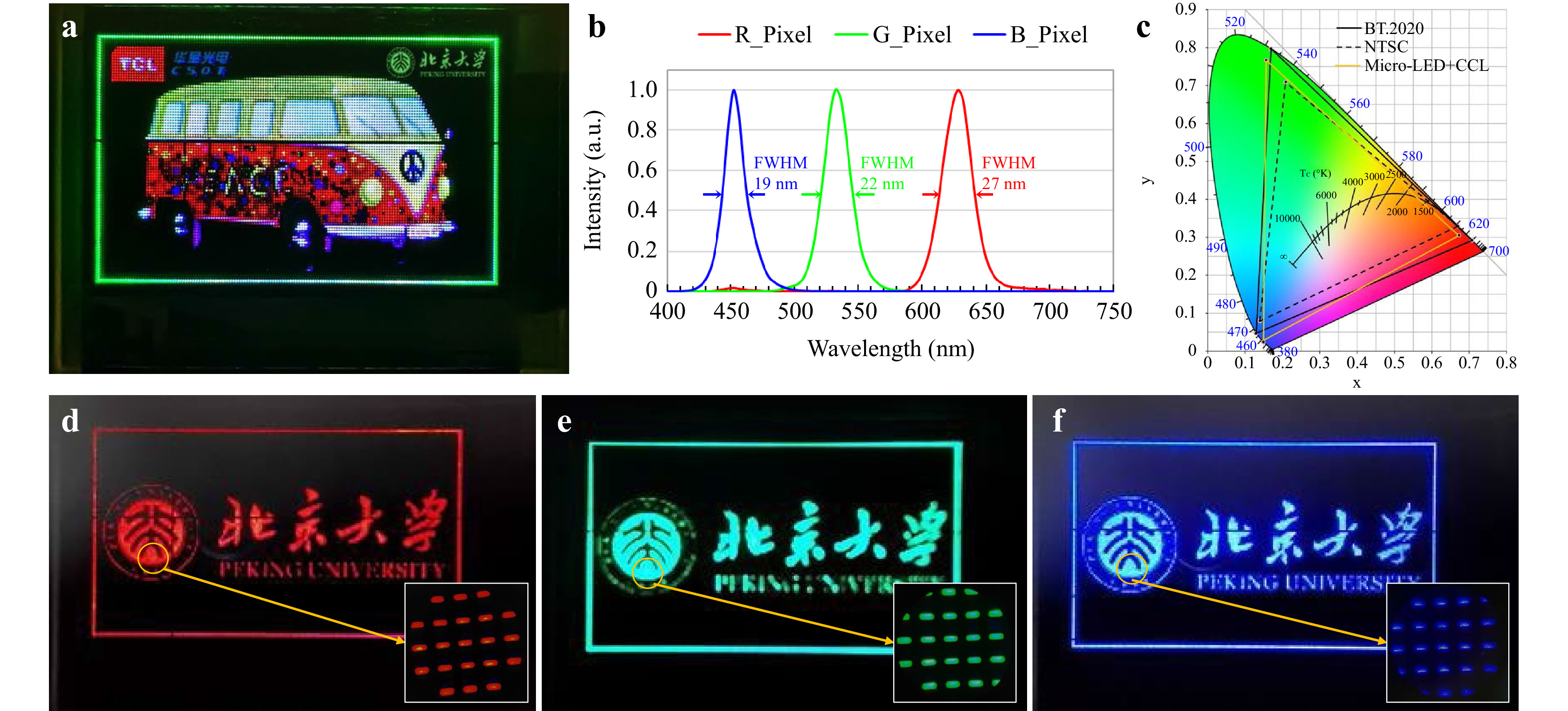
Fig. 5 Display performance of the manufactured display prototype. a Vivid bus image; d red, e green, and f blue Peking University logos illuminated by this CCLs-integrated micro-LED display (The insets in d, e and f are the corresponding microscopic images of red, green, and blue pixels). c EL and PL spectra of blue micro-LED and CCMs, respectively. d Color gamut of BT. 2020, NTSC standard, and our demonstrated module.
-
An efficient full-colour display prototype adopting a top-emitting blue micro-LED backlight integrated with CdSe QDs as the CCL was successfully manufactured. By employing a top-emitting backlight design with the space between each micro-LED chip filled with an LBM, the crosstalk effect between different pixels was efficiently alleviated. Compared with conventional micro-LED displays containing RGB LEDs, our developed display prototype offers significantly improved colour gamut values, as high as 122% NTSC or 91% BT.2020. This research provides an effective method for suppressing the crosstalk effect in top-emitting micro-LED-based displays. We anticipate that our proposed method will spur the further development of high-performance colour-converted full-colour micro-LED displays.
-
The TFT and CF plates were developed individually in two parallel steps. The TFT backplanes were obtained via a chain of cyclic procedures including sputtering, chemical vapour deposition, exposure, development, etching, and testing phases. The patterned CF and bank patterns were manufactured using conventional photolithography comprising coating, baking, exposing, and developing steps.
-
Micro-LED chips (100-μm-high with 85-μm-thick sapphire) were acquired from San’an Optoelectronics Co., Ltd. Active-matrix blue micro-LED backlights based on predeveloped TFT backplanes were fabricated in three main steps. In the first phase, tin (Sn) solder paste was deposited onto the pads (anodes and cathodes) using a printer combined with a metal stencil. Next, the micro-LED chips were moved onto the printed Sn patterns with proper electrode directions using a die bonder. In the final step, the panel was moved to an oven chamber to perform the reflow process. The LBM was created from thermosetting silica gel purchased from Tecore-Synchem Co., Ltd., Tianjin, China.
-
Both types of scatter ink and CdSe QDs were obtained from Suzhou Mesolight Nanotech Co., Ltd. The QD inks used were acrylic resin (tetradecyl acrylate, ~75 wt%), a photoinitiator (phenyl bis(2,4,6-trimethylbenzoyl)-phosphine oxide, 10 wt%), and QDs (~15 wt%). The QD component was exchanged with TiO2 spheres (diameter: ~200 nm) in the scatter ink for blue pixels. A programmable Dimatix Fujifilm DMP-2831 machine combined with a 10 pL cartridge was utilised to obtain patterned QD films. A customised voltage waveform was applied to eject a suitable ink volume. After the IJP process and after exposure to UV light (λ = 365 nm, intensity = 150 mJ/cm2) under a N2 environment for a duration of 5 min, 10-µm-thick QD films were obtained.
-
The crosstalk simulation was performed using Light Tools software. UV-Vis absorption and PL spectra were measured using a PerkinElmer Lambda 950 spectrophotometer and PerkinElmer LS 55 fluorescence spectrometer, respectively. A multichannel photometry detector equipped with a standard D65 source was used to obtain the transmittance spectra (Lambda Vision LVmicro Z, Japan). A FEI Scios system, operated at 10 kV, was used to capture the SEM images. A programmable spectrometer (Photo Research PR655) combined with a Keithley 2400 source meter was used to determine photoconversion performance. The brightness of the micro-LED displays was measured using a display colour analyser (Konica Minolta CA410). All the tests were conducted in an ambient atmosphere.
-
This work was financially supported by the Guangdong Basic and Applied Basic Research Foundation (No. 2021A1515110085), Key-Area Research and Development Program of Guangdong Province (No. 2019B010924003), Shenzhen Hong Kong Innovation Circle Joint R&D Project (SGDX20190918105201704), Shenzhen Fundamental Research Program (No. GXWD20201231165807007-20200810113811001), and Shenzhen Science and Technology Research Grant (JCYJ20170818085627903).
Alleviating the crosstalk effect via a fine-moulded light-blocking matrix for colour-converted micro-LED display with a 122% NTSC gamut
- Yongming Yin1,
- Zhiping Hu1, 2,
- Muhammad Umair Ali1, 3,
- Miao Duan4,
- Yongwei Wu4,
- Ming Liu1,
- Wenxiang Peng4,
- Jun Hou4,
- Dongze Li4,
- Xin Zhang4,
-
Hong Meng1, *, ,

- Light: Advanced Manufacturing 3, Article number: (2022)
- Received: 24 November 2021
- Revised: 17 May 2022
- Accepted: 17 May 2022 Published online: 06 June 2022
doi: https://doi.org/10.37188/lam.2022.036
Abstract: One of the major challenges when fabricating high gamut colour-converted micro-light-emitting diodes (LEDs) displays is severe crosstalk effect among adjacent pixels because of the wide view-angle feature of micro-LED chips. In this study, potential factors that contribute to the crosstalk effect were systematically simulated. We observed that precisely filling the space between each micro-LED chip with a light blocking matrix (LBM) can be a promising solution to alleviate this risk. After careful investigations, a press-assisted moulding technique was demonstrated to be an effective approach of fabricating the LBM. Nevertheless, experimental observations further revealed that residual black LBM on the surface of micro-LEDs severely reduces the brightness, thereby compromising the display performance. This problem was successfully addressed by employing a plasma etching technique to efficiently extract the trapped light. Eventually, a top-emitting blue micro-LED-based backlight fine-moulded with a black LBM was developed and combined with red and green quantum dot colour-conversion layers for full-colour display. The colour gamut of our manufactured display prototype can cover as high as 122% that of the National Television Standards Committee.
Research Summary
High gamut colour-converted full-colour micro-LED display
In this study, potential factors that contribute to the crosstalk effect were systematically simulated. We observed that precisely filling the space between each micro-LED chip with a light blocking matrix (LBM) can be a promising solution to alleviate this risk. After careful investigations, a press-assisted moulding technique was demonstrated to be an effective approach of fabricating the LBM. Nevertheless, experimental observations further revealed that residual black LBM on the surface of micro-LEDs severely reduces the brightness, thereby compromising the display performance. This problem was successfully addressed by employing a plasma etching technique to efficiently extract the trapped light. Eventually, a top-emitting blue micro-LED-based backlight fine-moulded with a black LBM was developed and combined with red and green quantum dot colour-conversion layers for full-colour display. The colour gamut of our manufactured display prototype can cover as high as 122% that of the National Television Standards Committee.
Rights and permissions
Open Access This article is licensed under a Creative Commons Attribution 4.0 International License, which permits use, sharing, adaptation, distribution and reproduction in any medium or format, as long as you give appropriate credit to the original author(s) and the source, provide a link to the Creative Commons license, and indicate if changes were made. The images or other third party material in this article are included in the article′s Creative Commons license, unless indicated otherwise in a credit line to the material. If material is not included in the article′s Creative Commons license and your intended use is not permitted by statutory regulation or exceeds the permitted use, you will need to obtain permission directly from the copyright holder. To view a copy of this license, visit http://creativecommons.org/licenses/by/4.0/.

 DownLoad: