
2024 Vol. 5, No. 3
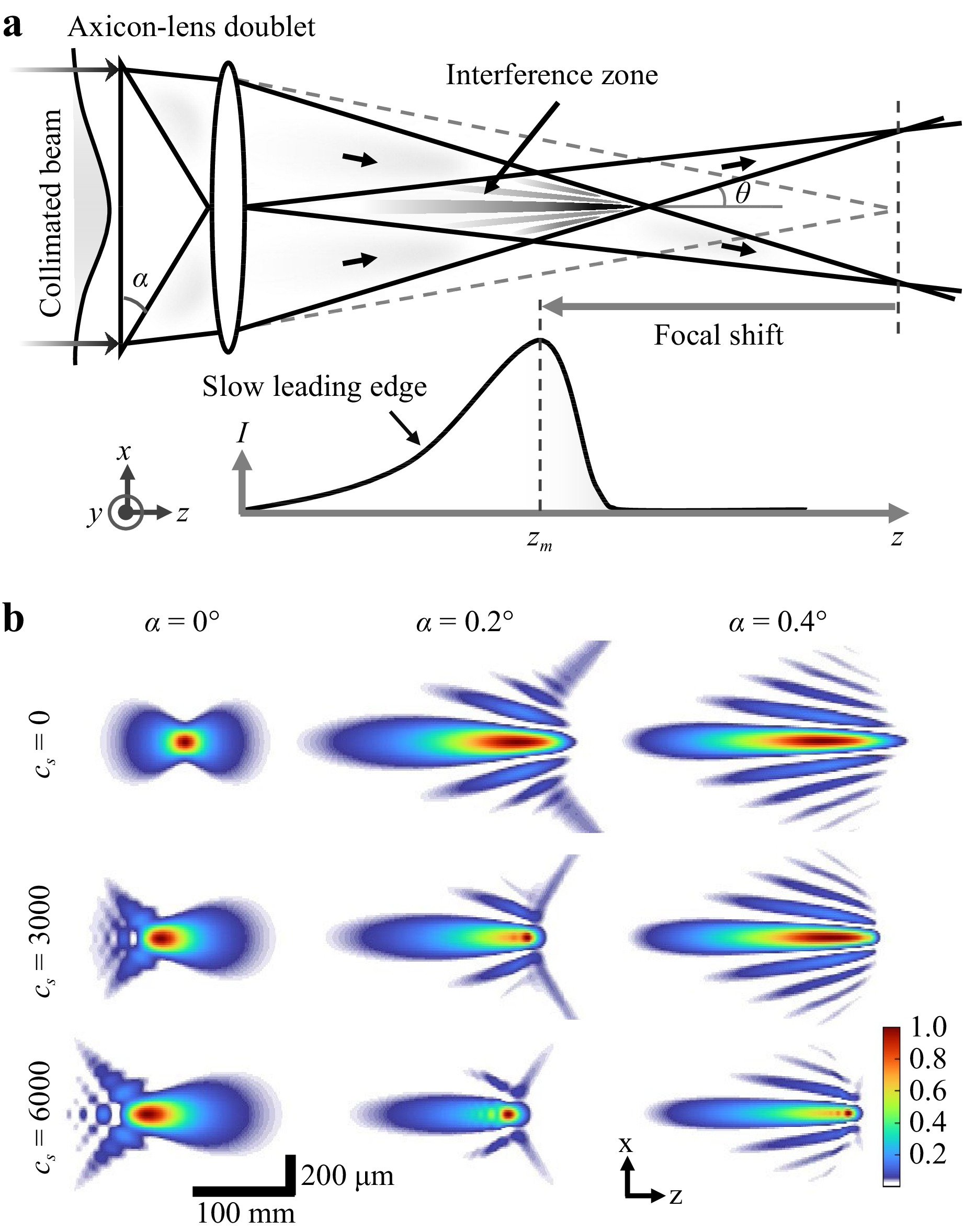
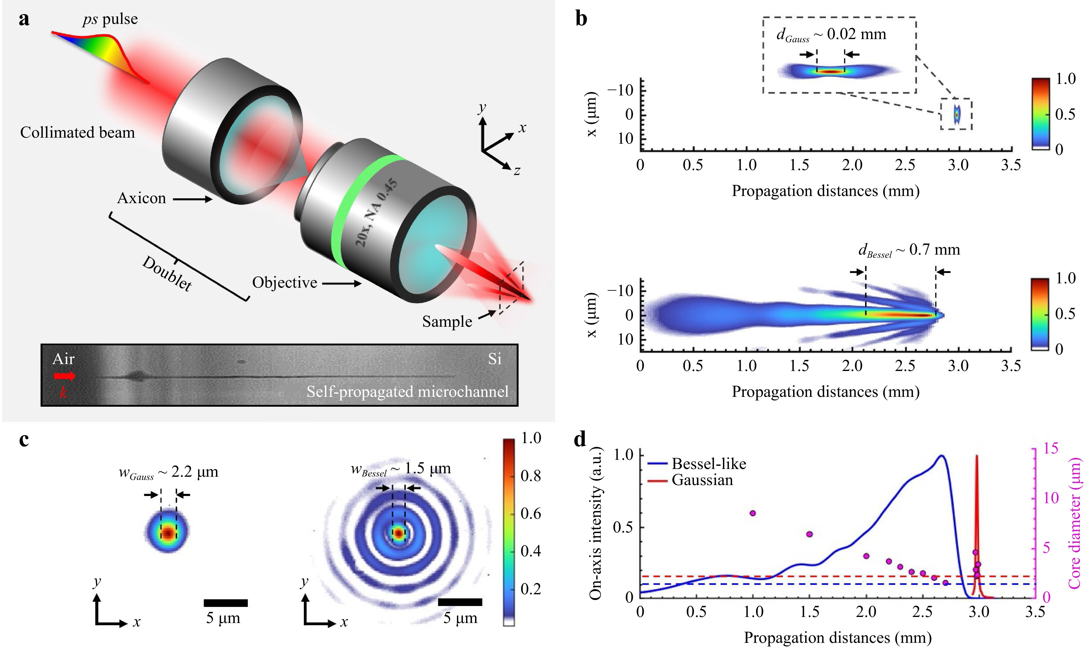
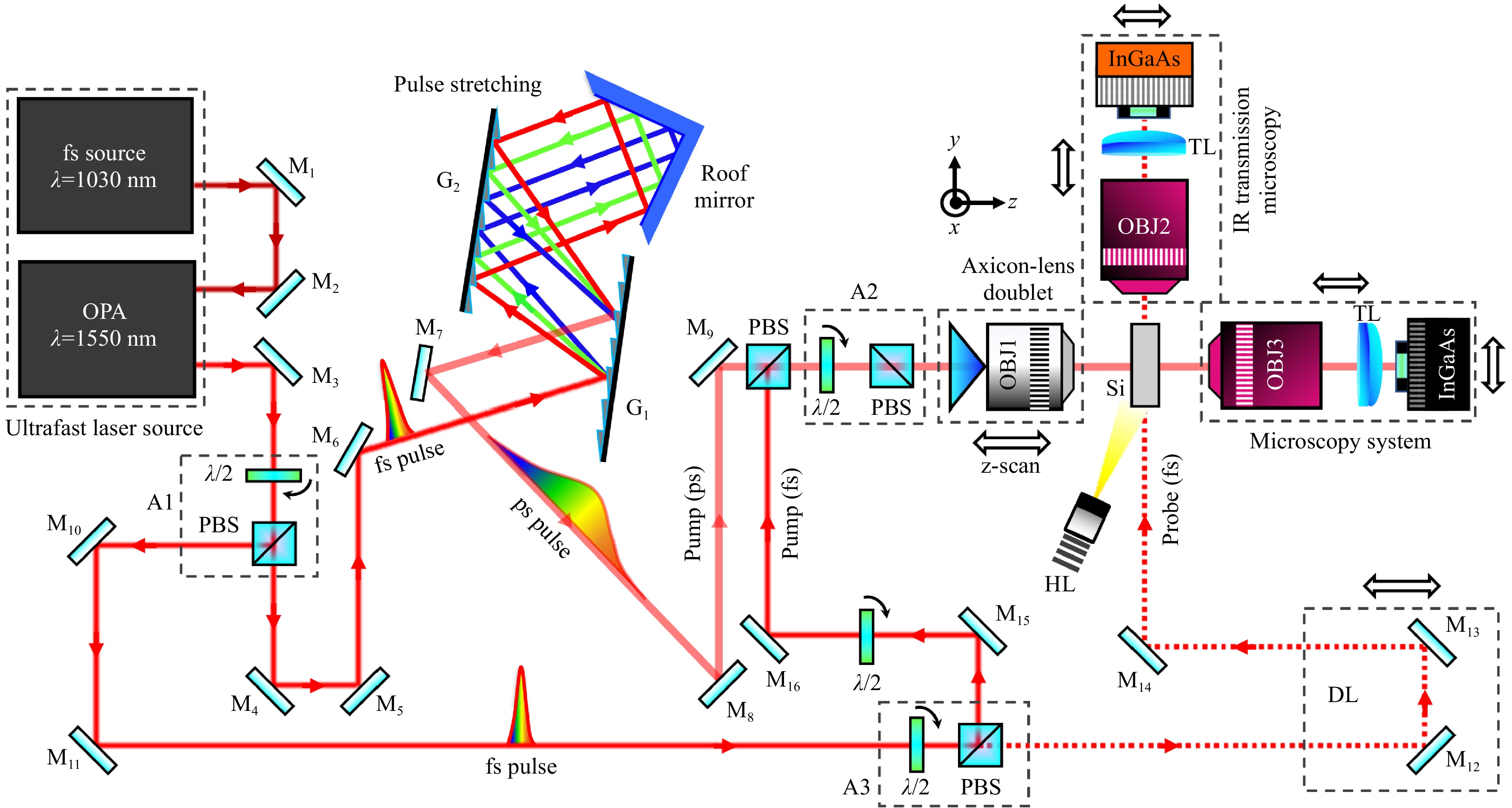
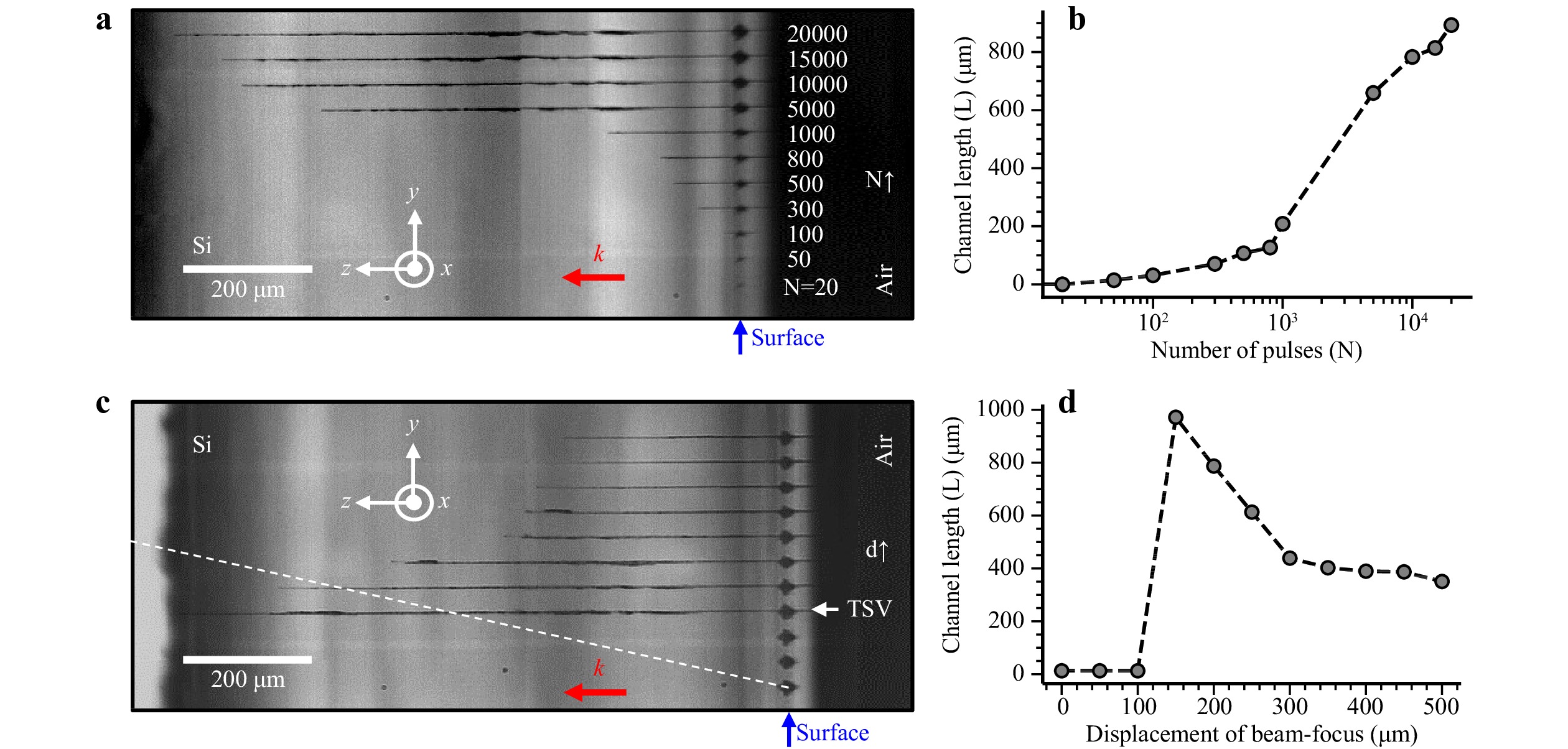
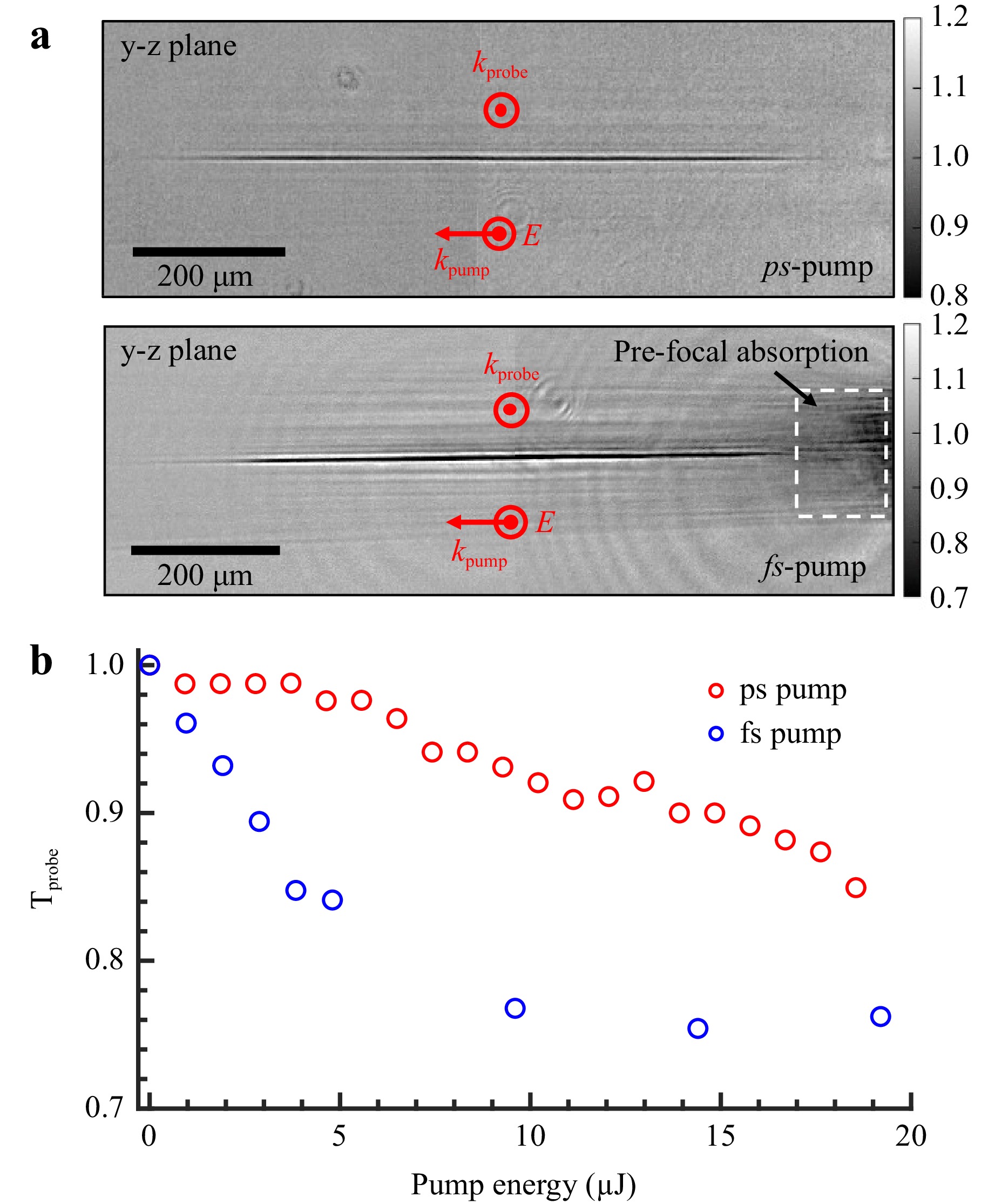
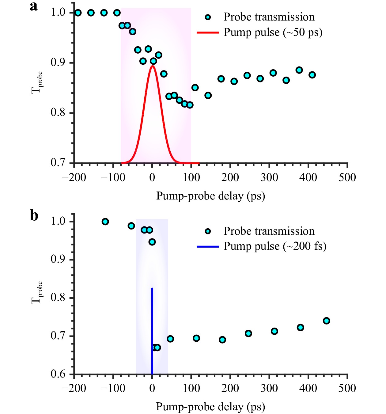
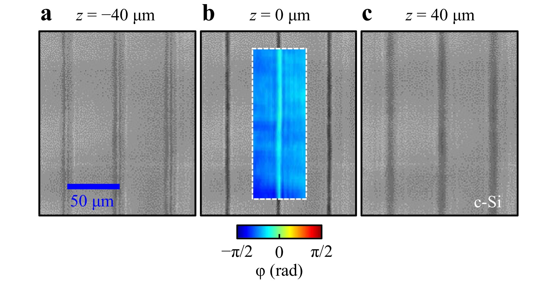
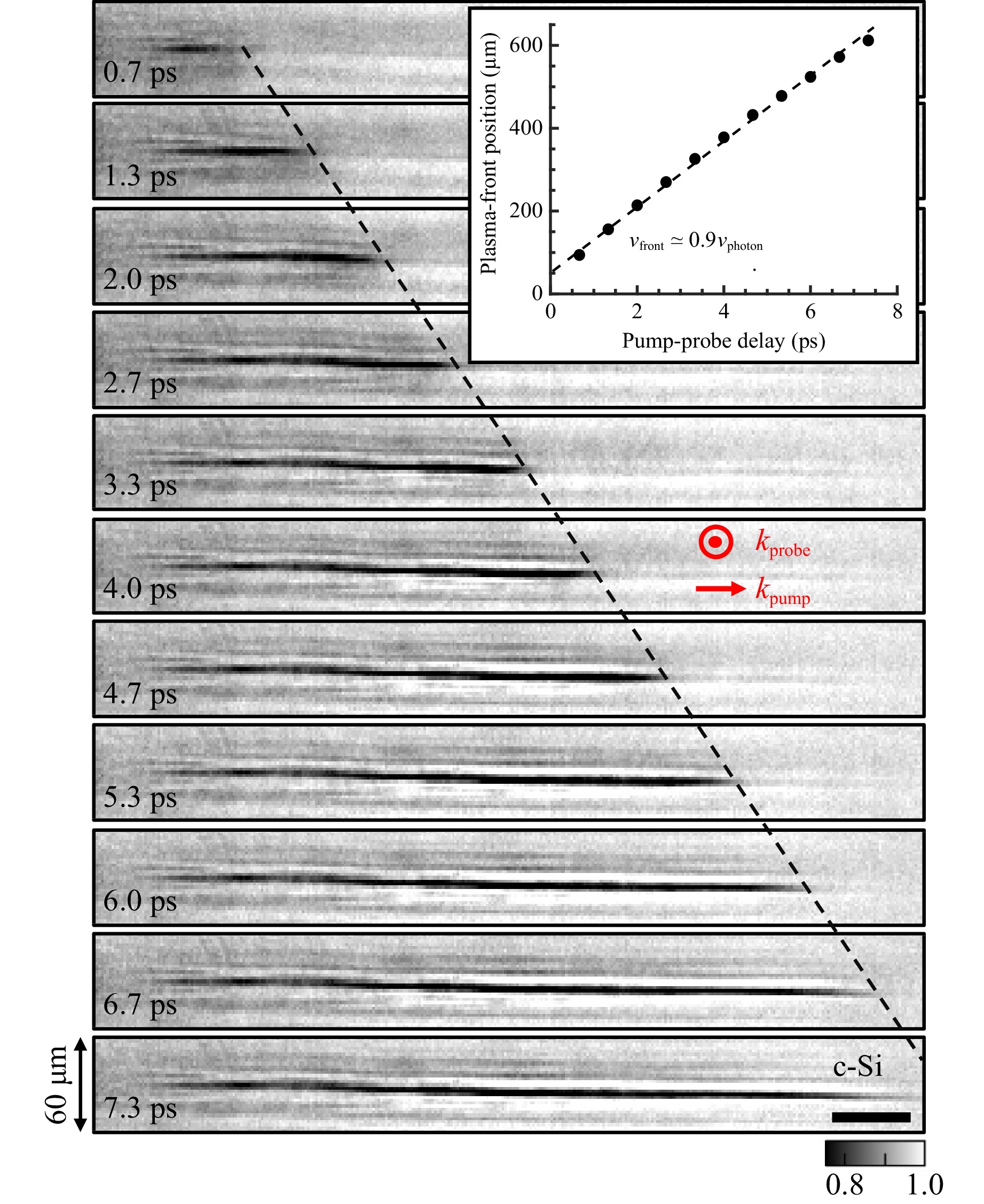
We describe how a direct combination of an axicon and a lens can represent a simple and efficient beam-shaping solution for laser material processing applications. We produce high-angle pseudo-Bessel micro-beams at 1550 nm, which would be difficult to produce by other methods. Combined with appropriate stretching of femtosecond pulses, we access optimized conditions inside semiconductors allowing us to develop high-aspect-ratio refractive-index writing methods. Using ultrafast microscopy techniques, we characterize the delivered local intensities and the triggered ionization dynamics inside silicon with 200-fs and 50-ps pulses. While similar plasma densities are produced in both cases, we show that repeated picosecond irradiation induces permanent modifications spontaneously growing shot-after-shot in the direction of the laser beam from front-surface damage to the back side of irradiated silicon wafers. The conditions for direct microexplosion and microchannel drilling similar to those today demonstrated for dielectrics still remain inaccessible. Nonetheless, this work evidences higher energy densities than those previously achieved in semiconductors and a novel percussion writing modality to create structures in silicon with aspect ratios exceeding ~700 without any motion of the beam. The estimated transient change of conductivity and measured ionization fronts at near luminal speed along the observed microplasma channels support the vision of vertical electrical connections optically controllable at GHz repetition rates. The permanent silicon modifications obtained by percussion writing are light-guiding structures according to a measured positive refractive index change exceeding 10−2. These findings open the door to unique monolithic solutions for electrical and optical through-silicon-vias which are key elements for vertical interconnections in 3D chip stacks.
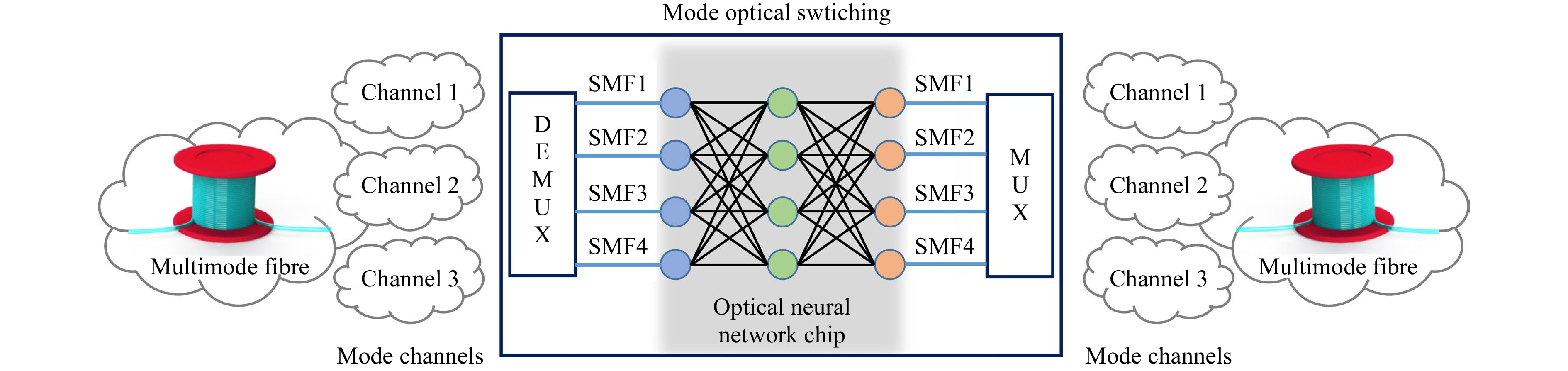
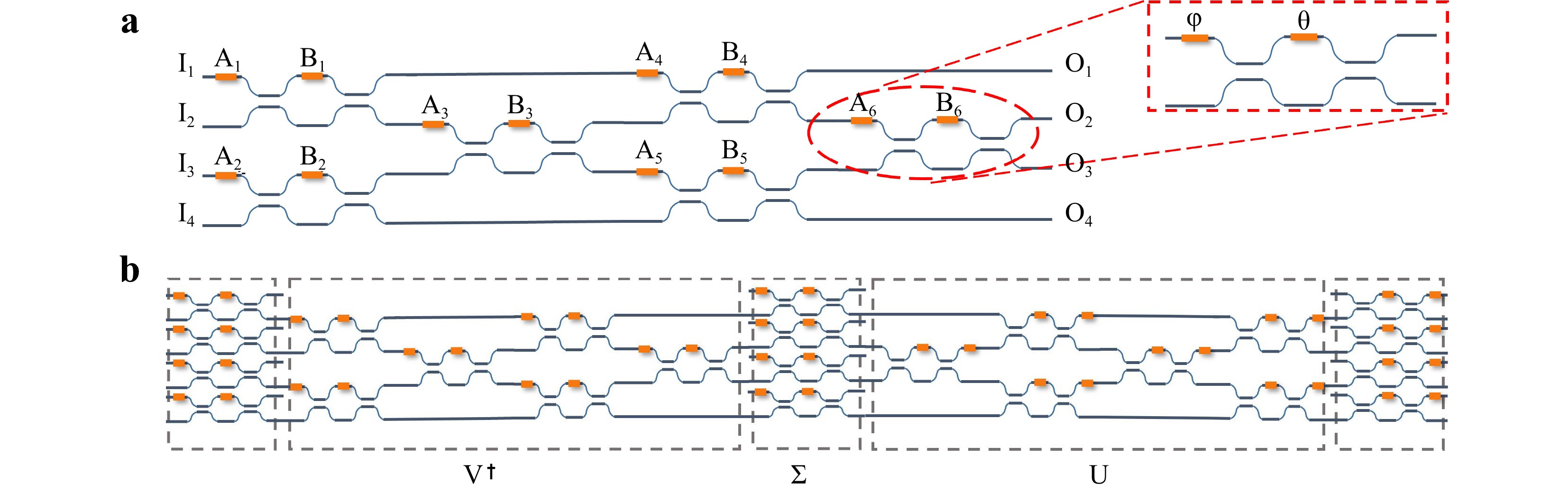
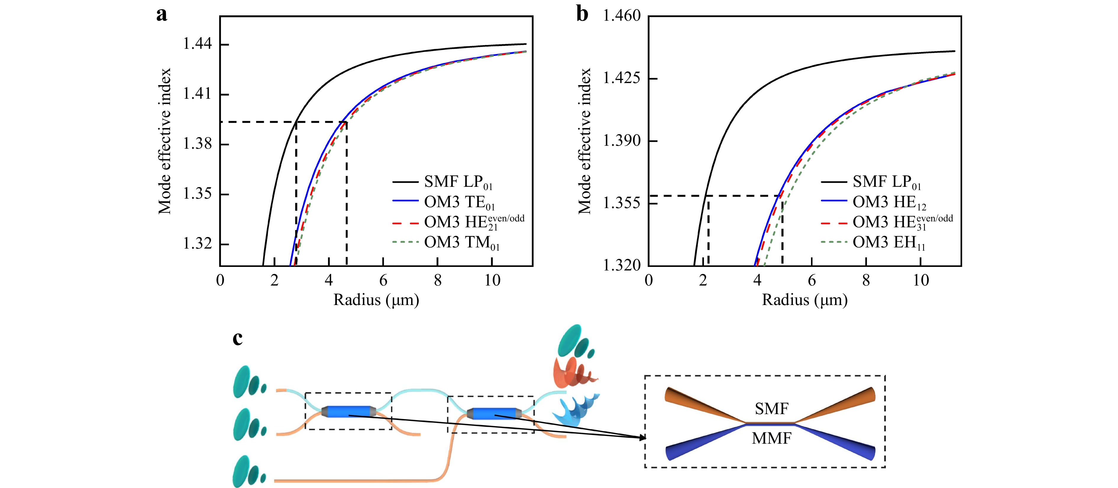
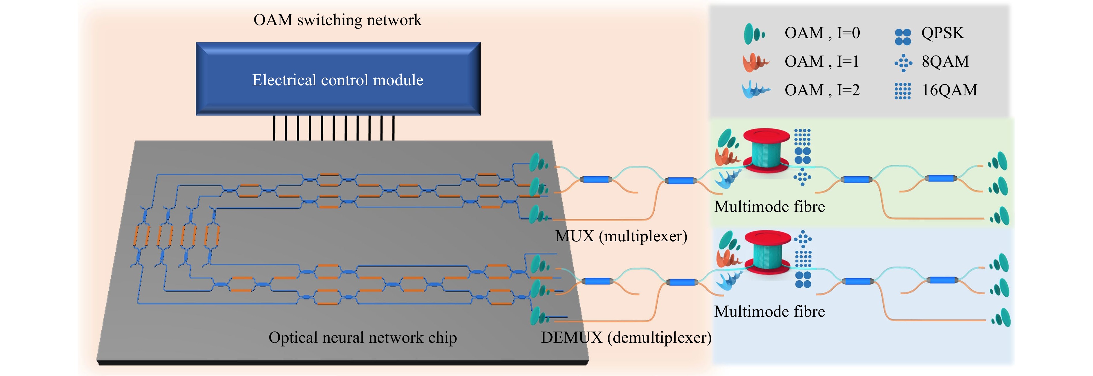
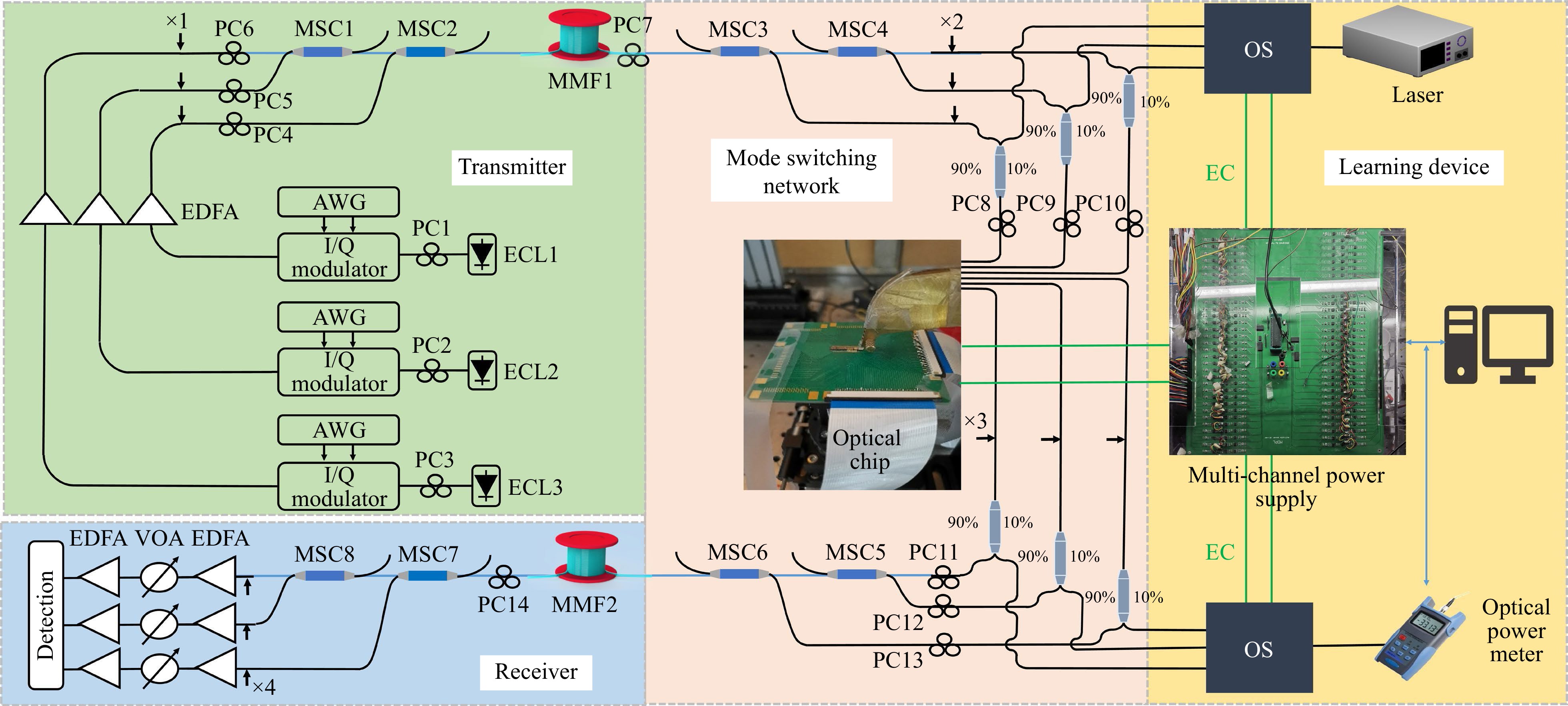
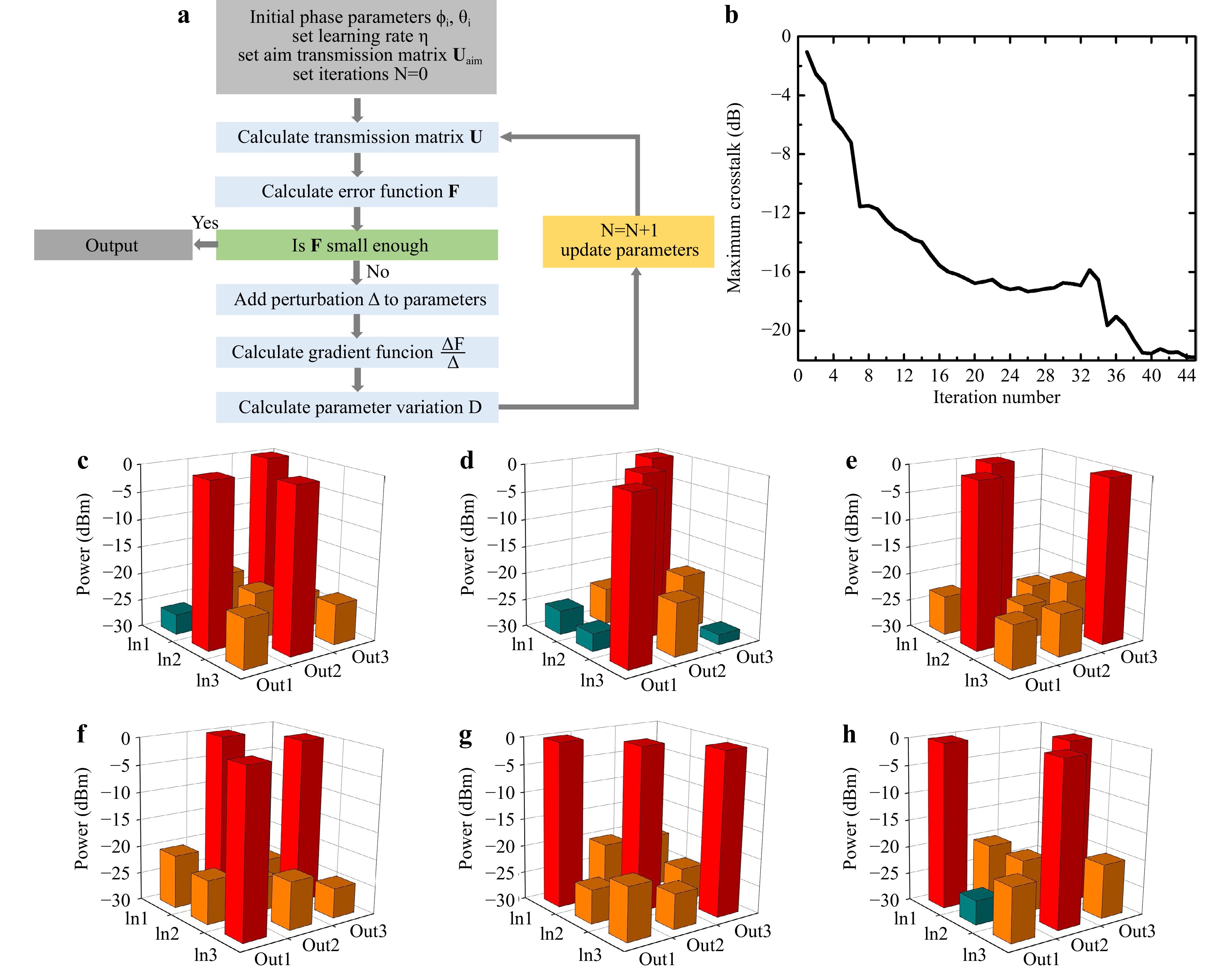
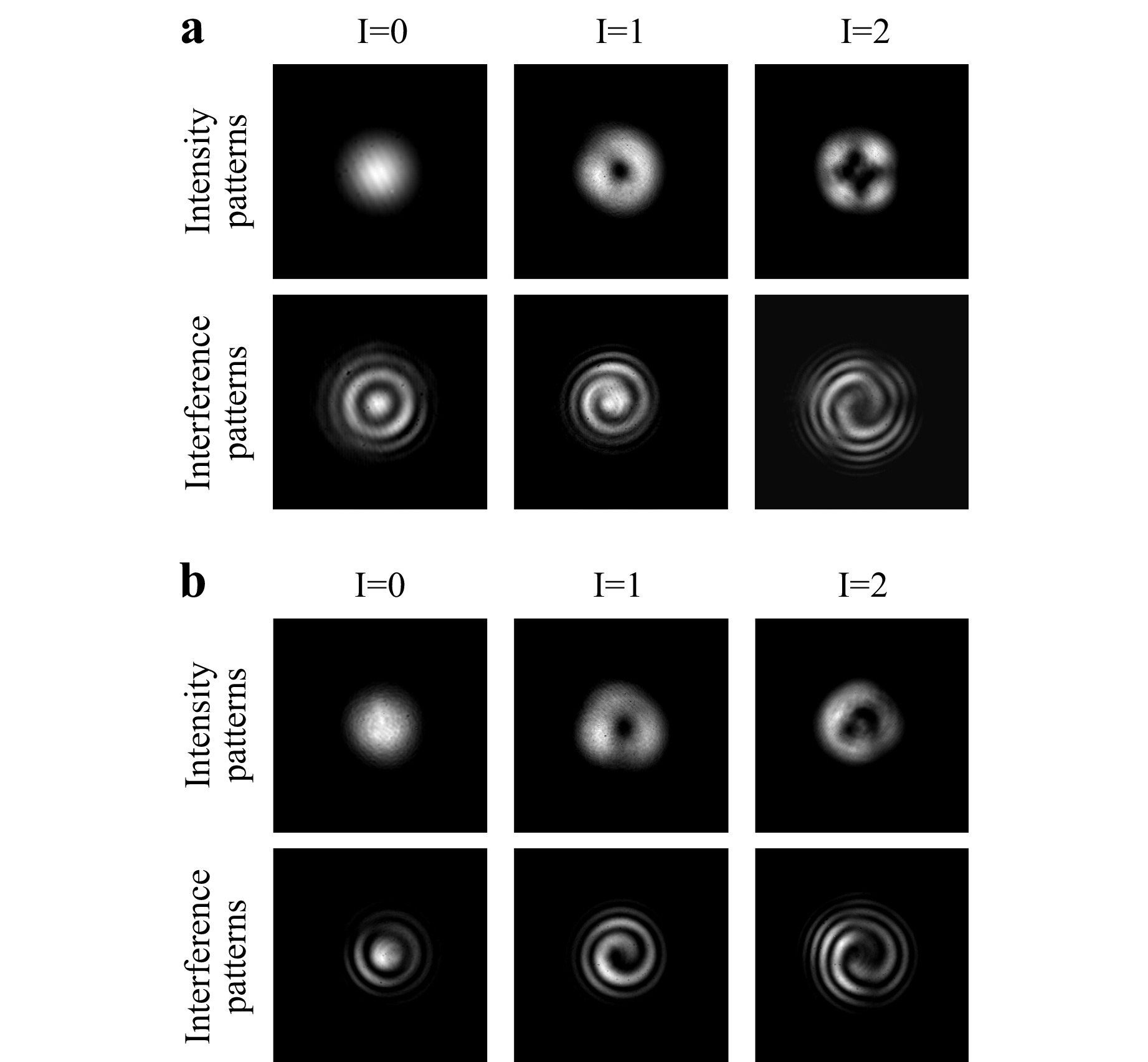
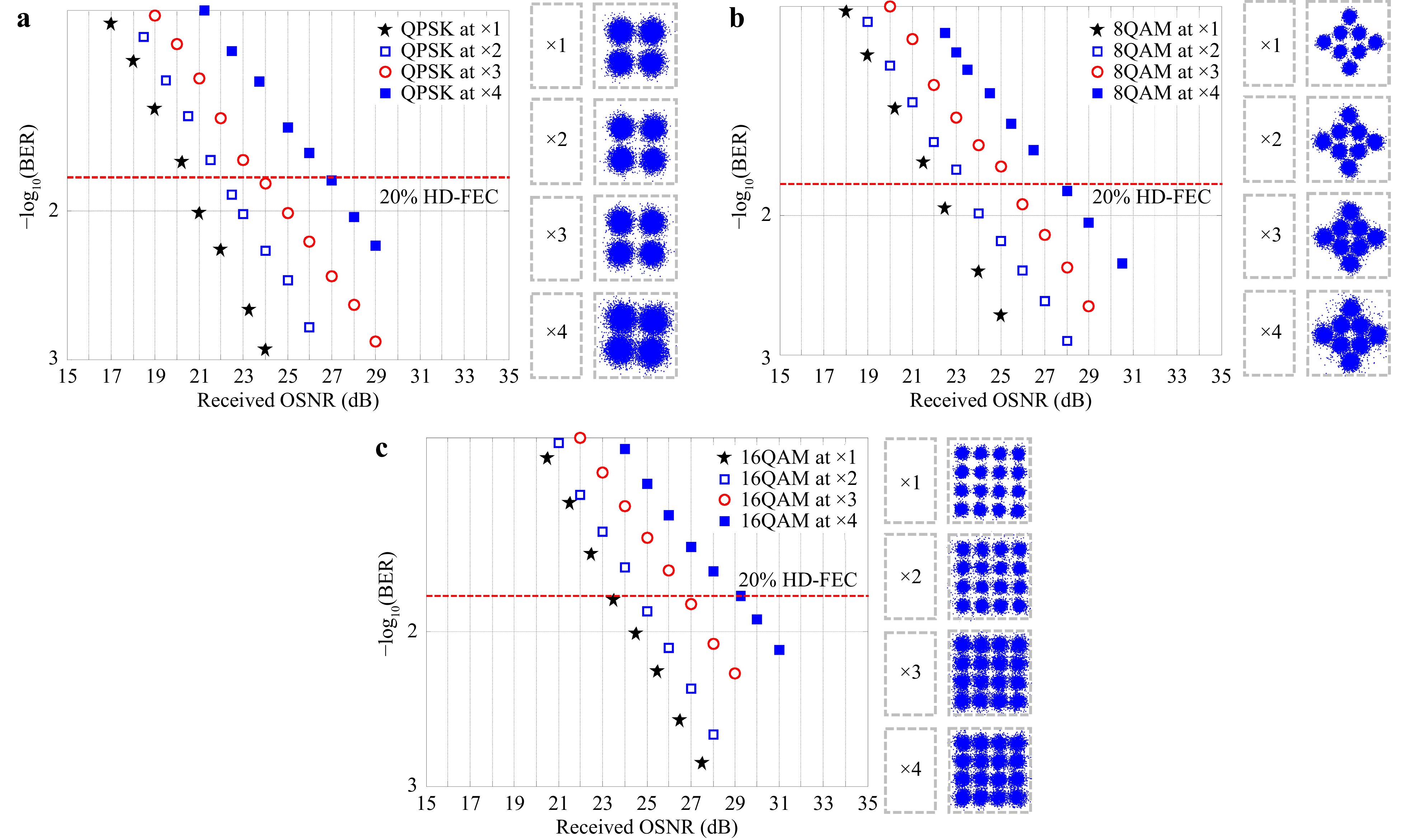
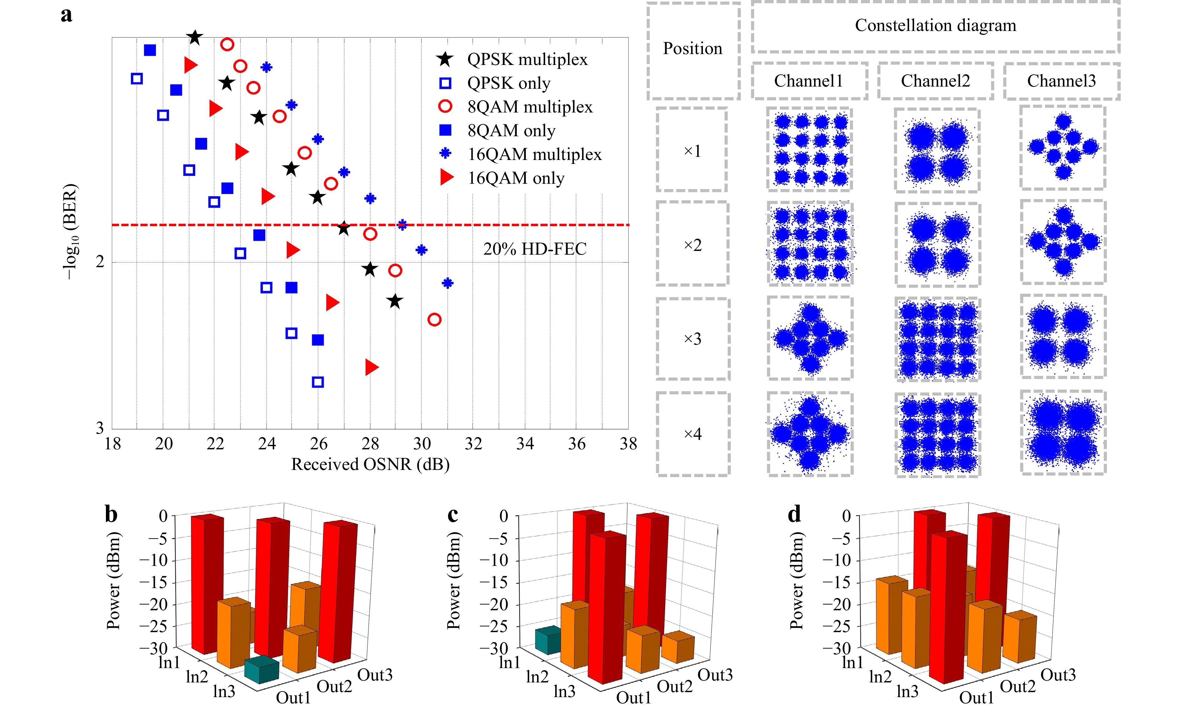
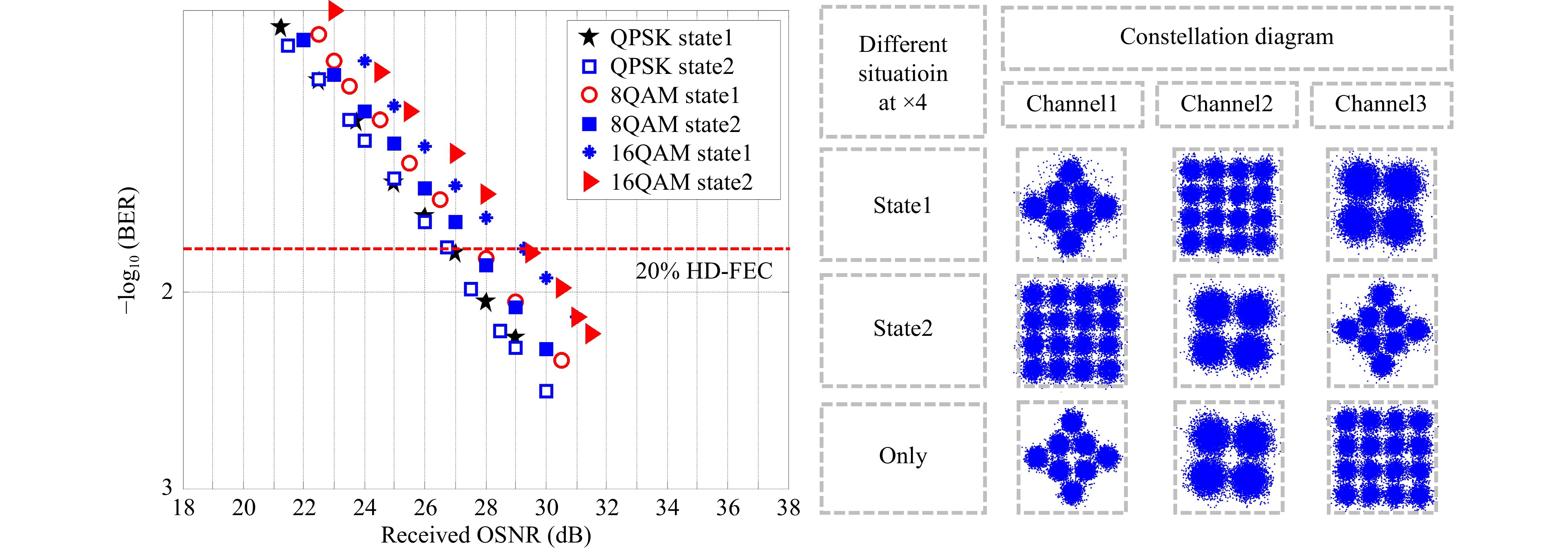
Mode-division multiplexing technology has been proposed as a crucial technique for enhancing communication capacity and alleviating growing communication demands. Optical switching, which is an essential component of optical communication systems, enables information exchange between channels. However, existing optical switching solutions are inadequate for addressing flexible information exchange among the mode channels. In this study, we introduced a flexible mode switching system in a multimode fibre based on an optical neural network chip. This system utilised the flexibility of on-chip optical neural networks along with an all-fibre orbital angular momentum (OAM) mode multiplexer-demultiplexer to achieve mode switching among the three OAM modes within a multimode fibre. The system adopted an improved gradient descent algorithm to achieve training for arbitrary 3 × 3 exchange matrices and ensured maximum crosstalk of less than −18.7 dB, thus enabling arbitrary inter-mode channel information exchange. The proposed optical-neural-network-based mode-switching system was experimentally validated by successfully transmitting different modulation formats across various modes. This innovative solution holds promise for providing effective optical switching in practical multimode communication networks.
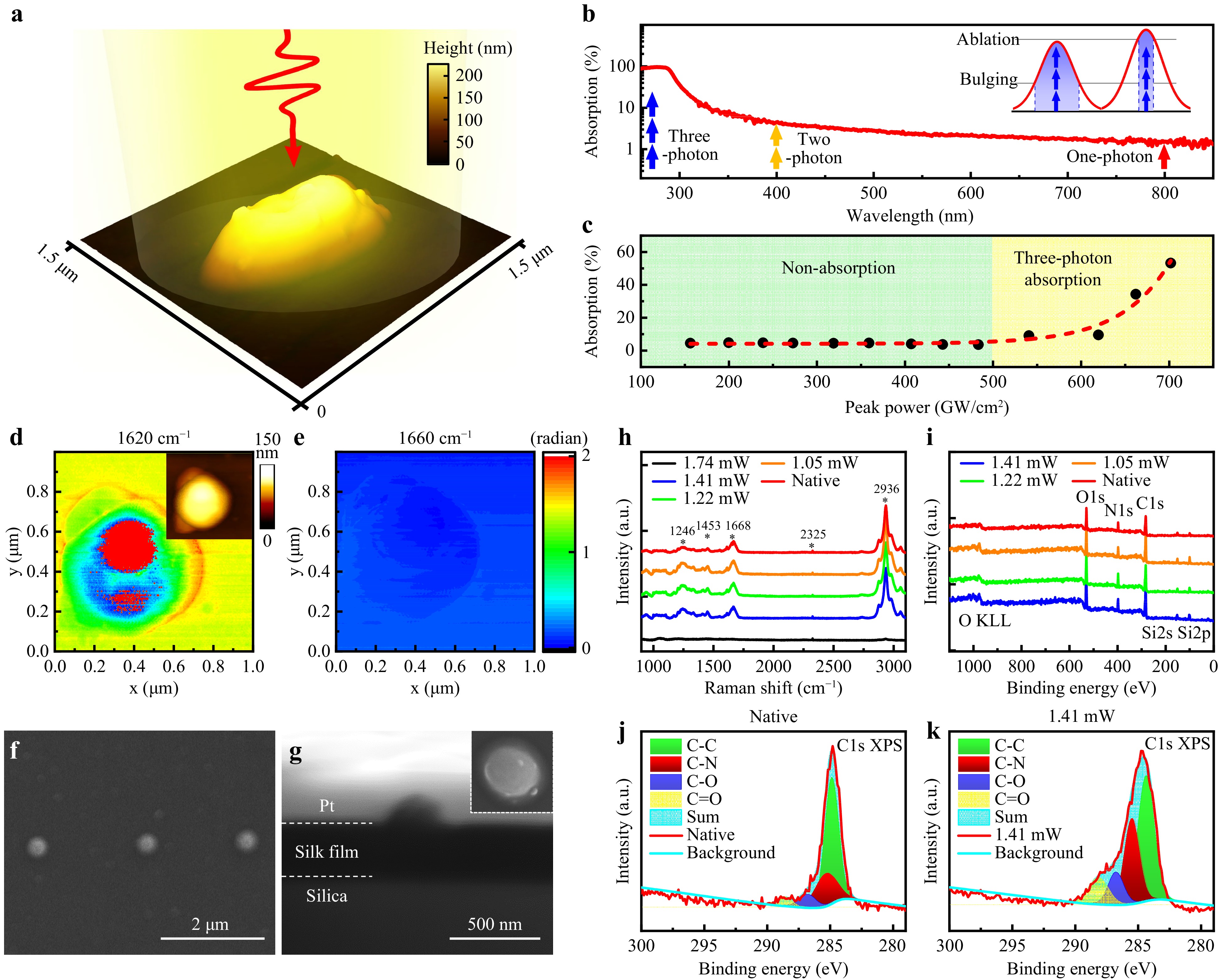
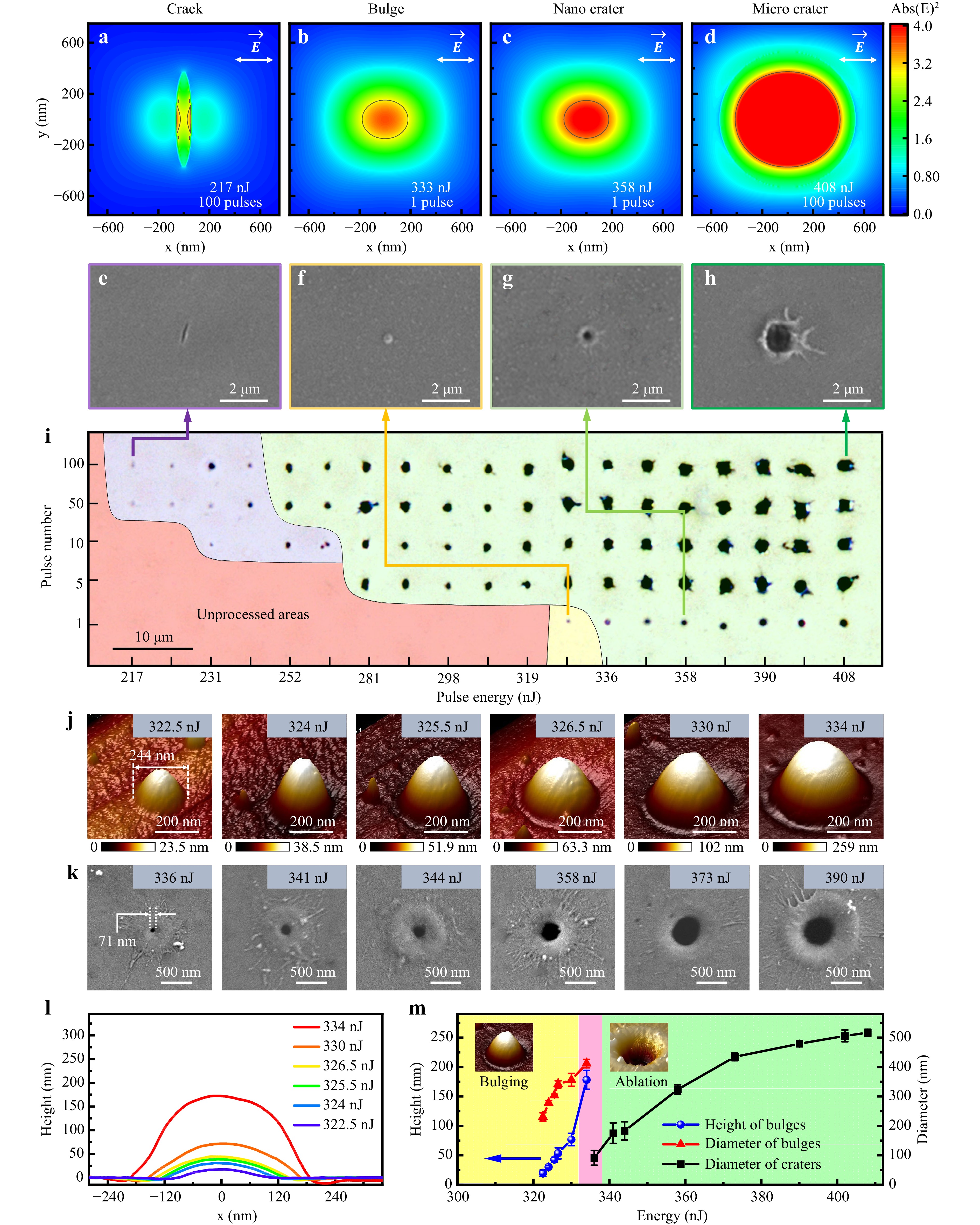
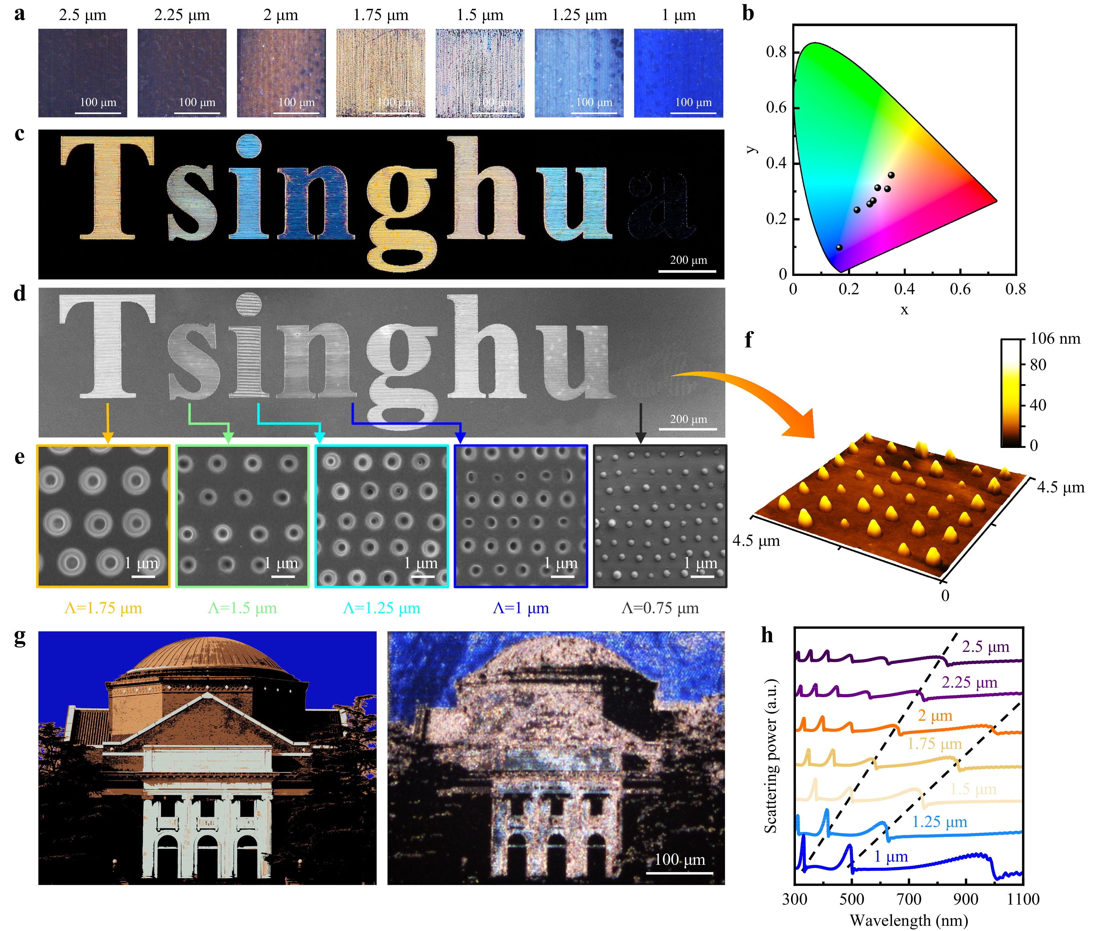
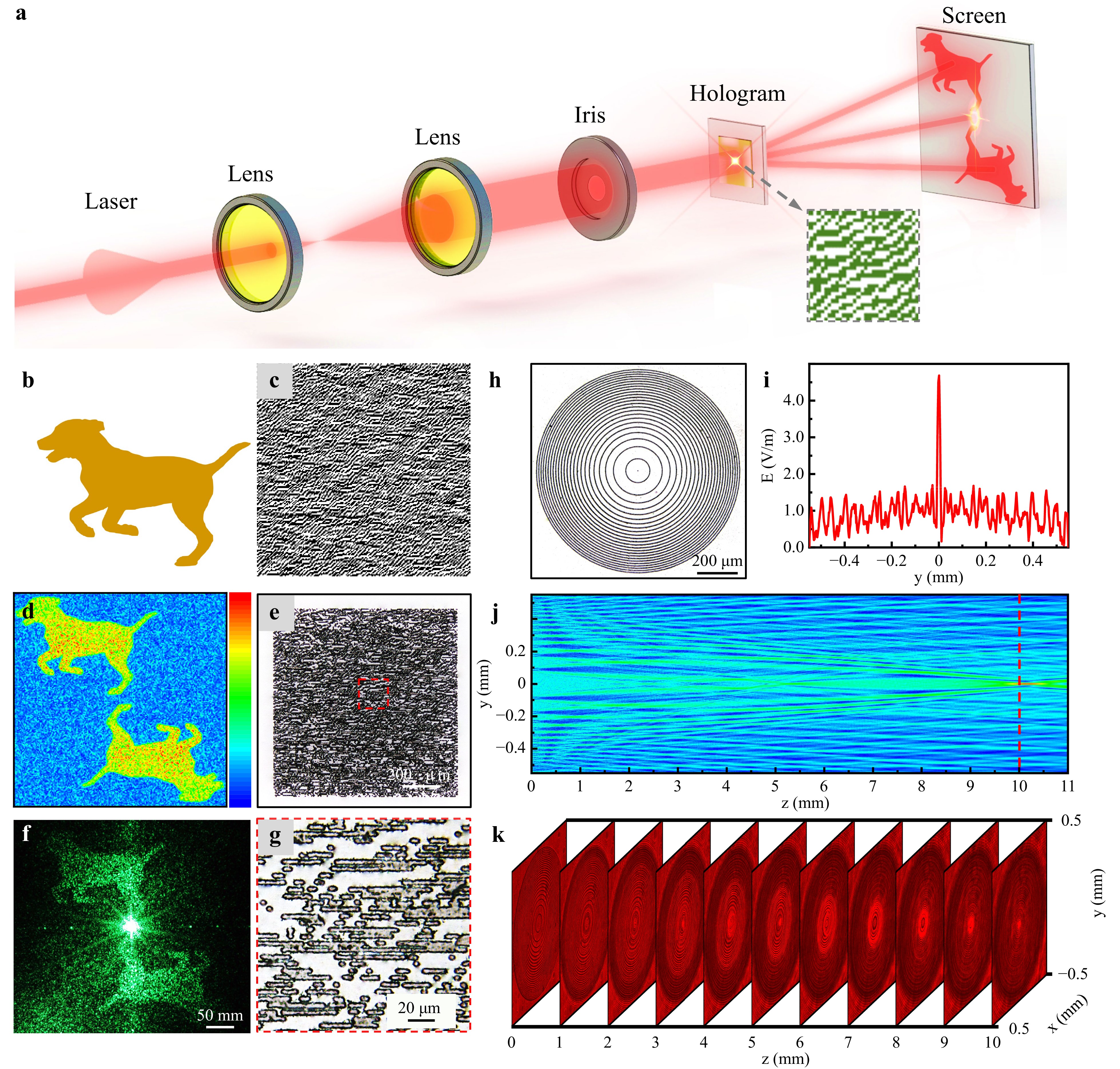
Organic proteins are attractive owing to their unique optical properties, remarkable mechanical characteristics, and biocompatibility. Manufacturing multifunctional structures on organic protein films is essential for practical applications; however, the controllable fabrication of specific structures remains challenging. Herein, we propose a strategy for creating specific structures on silk film surfaces by modulating the bulging and ablation of organic materials. Unique surface morphologies such as bulges and craters with continuously varying diameters were generated based on the controlled ultrafast laser-induced crystal-form transition and plasma ablation of the silk protein. Owing to the anisotropic optical properties of the bulge/crater structures with different periods, the fabricated organic films can be used for large-scale inkless color printing. By simultaneously engineering bulge/crater structures, we designed and demonstrated organic film-based optical functional devices that achieves holographic imaging and optical focusing. This study provides a promising strategy for the fabrication of multifunctional micro/nanostructures that can broaden the potential applications of organic materials.
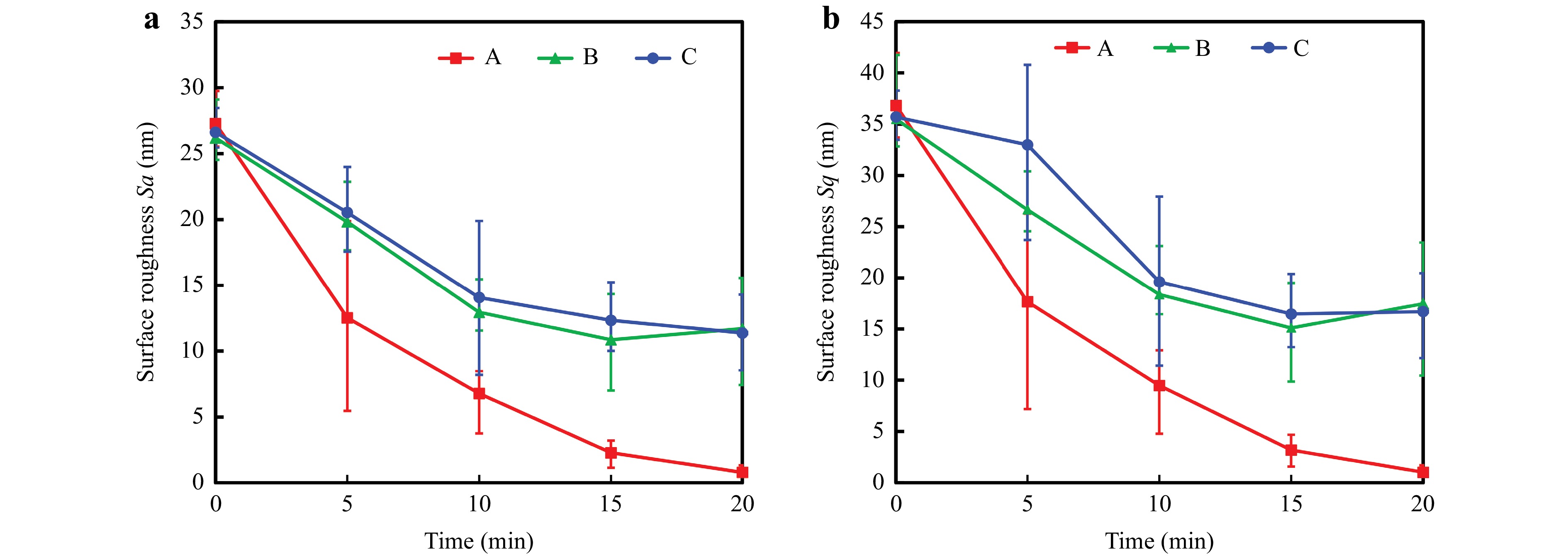
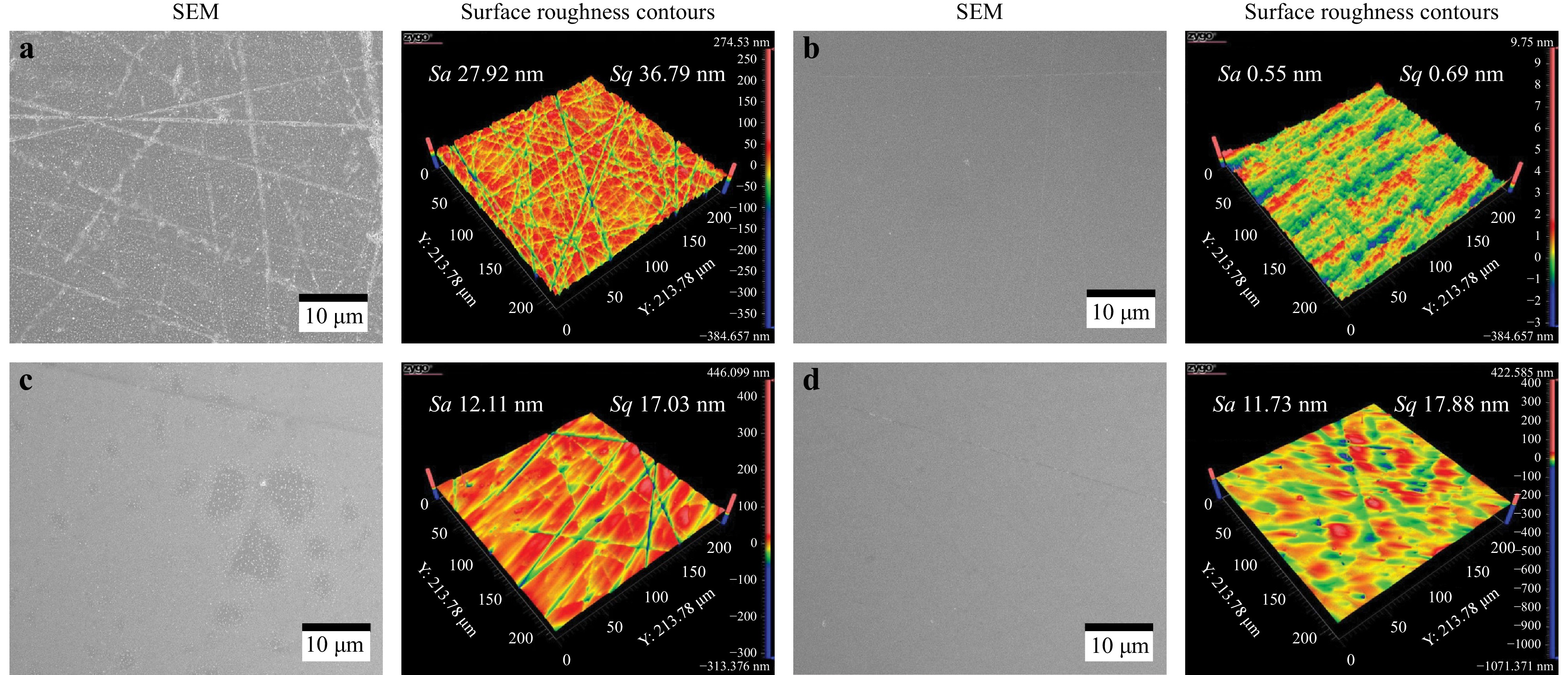
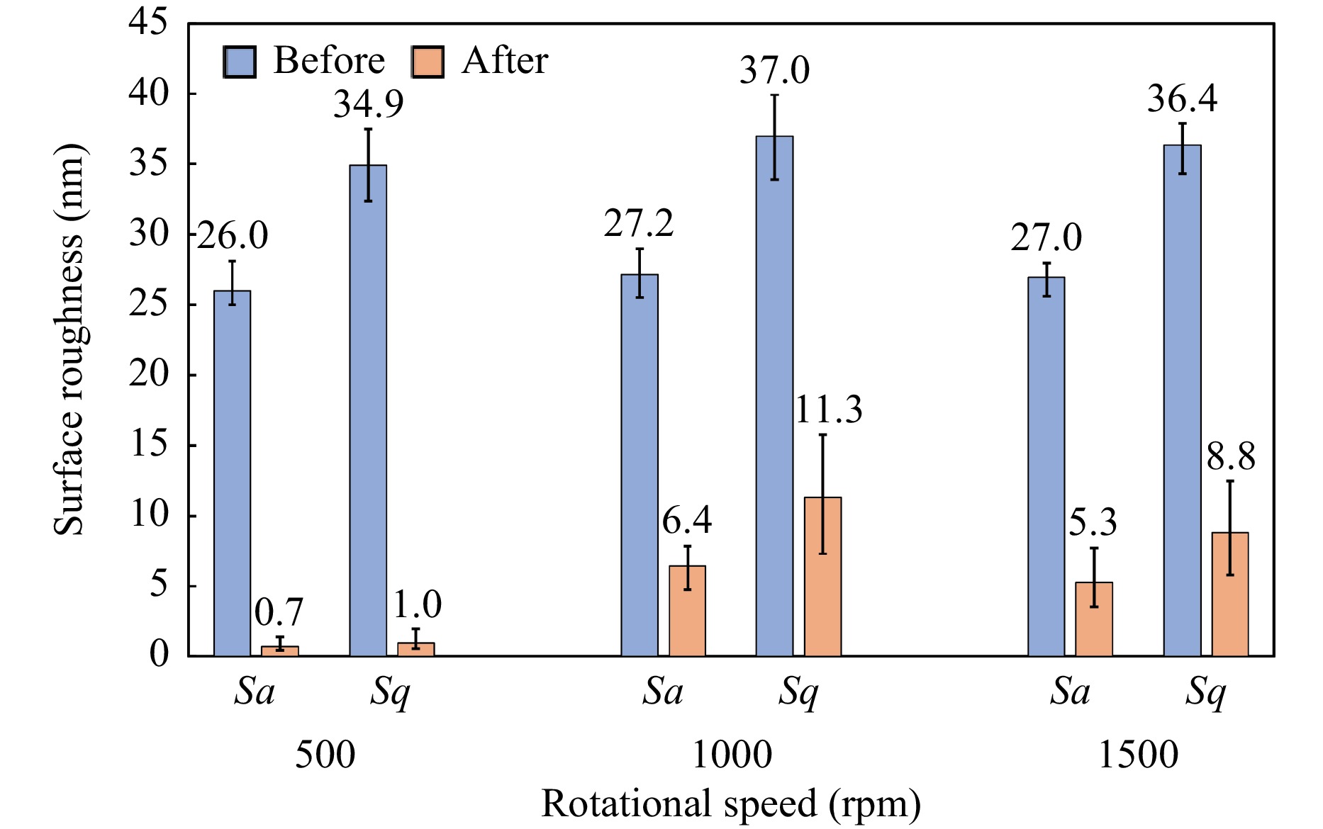
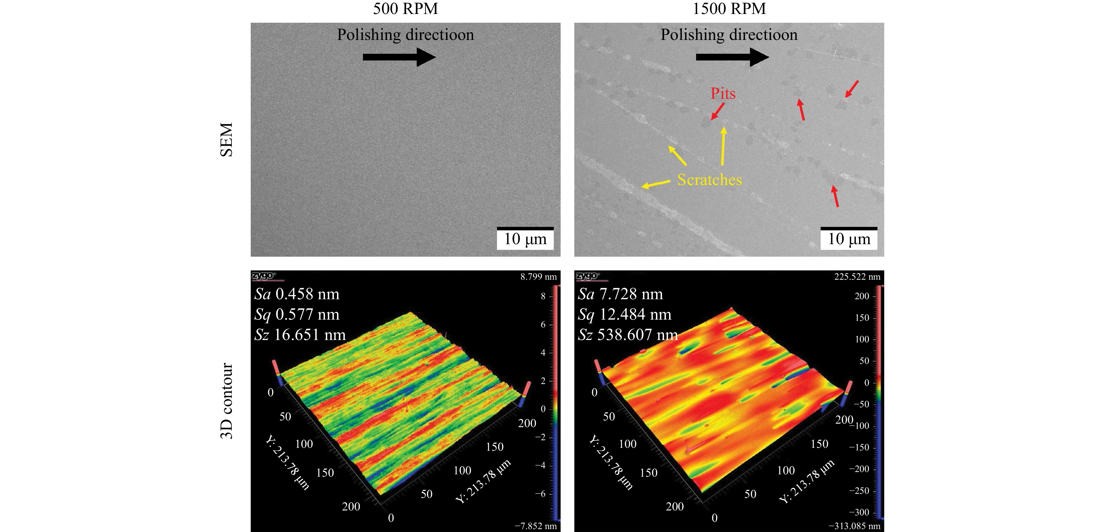
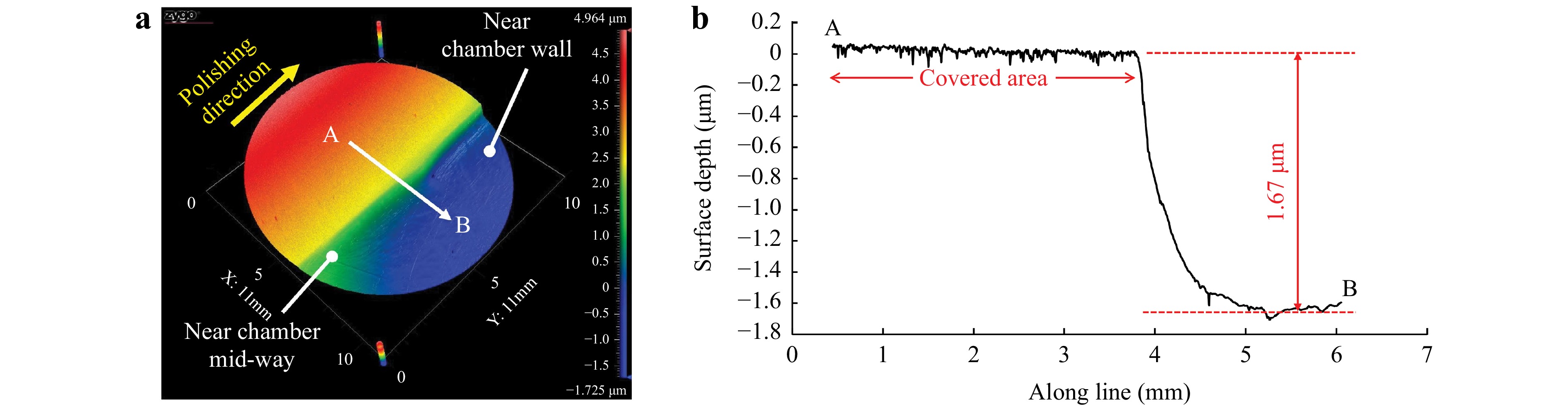
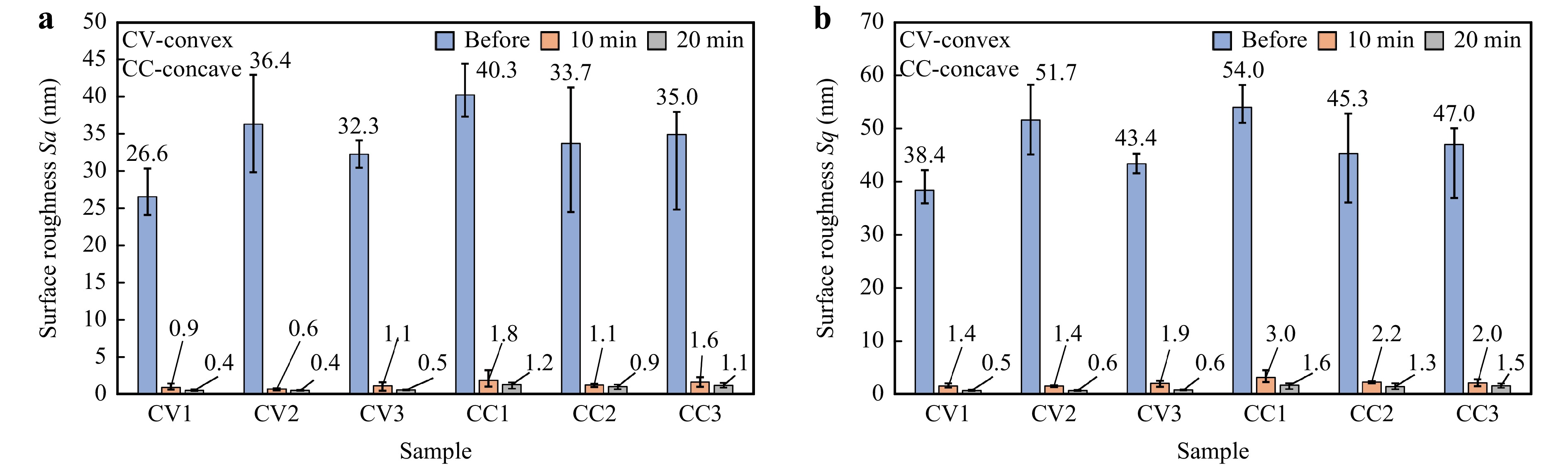
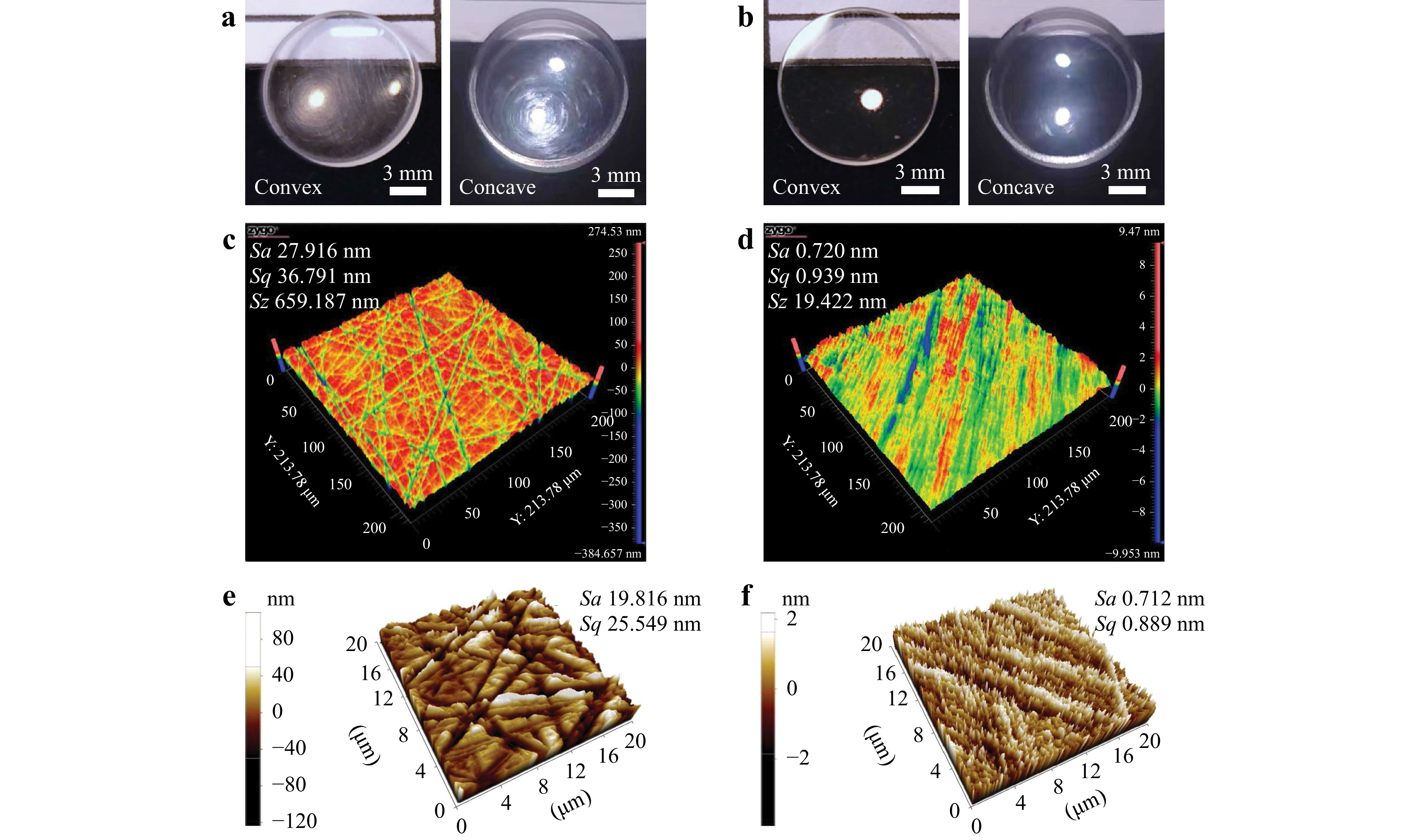
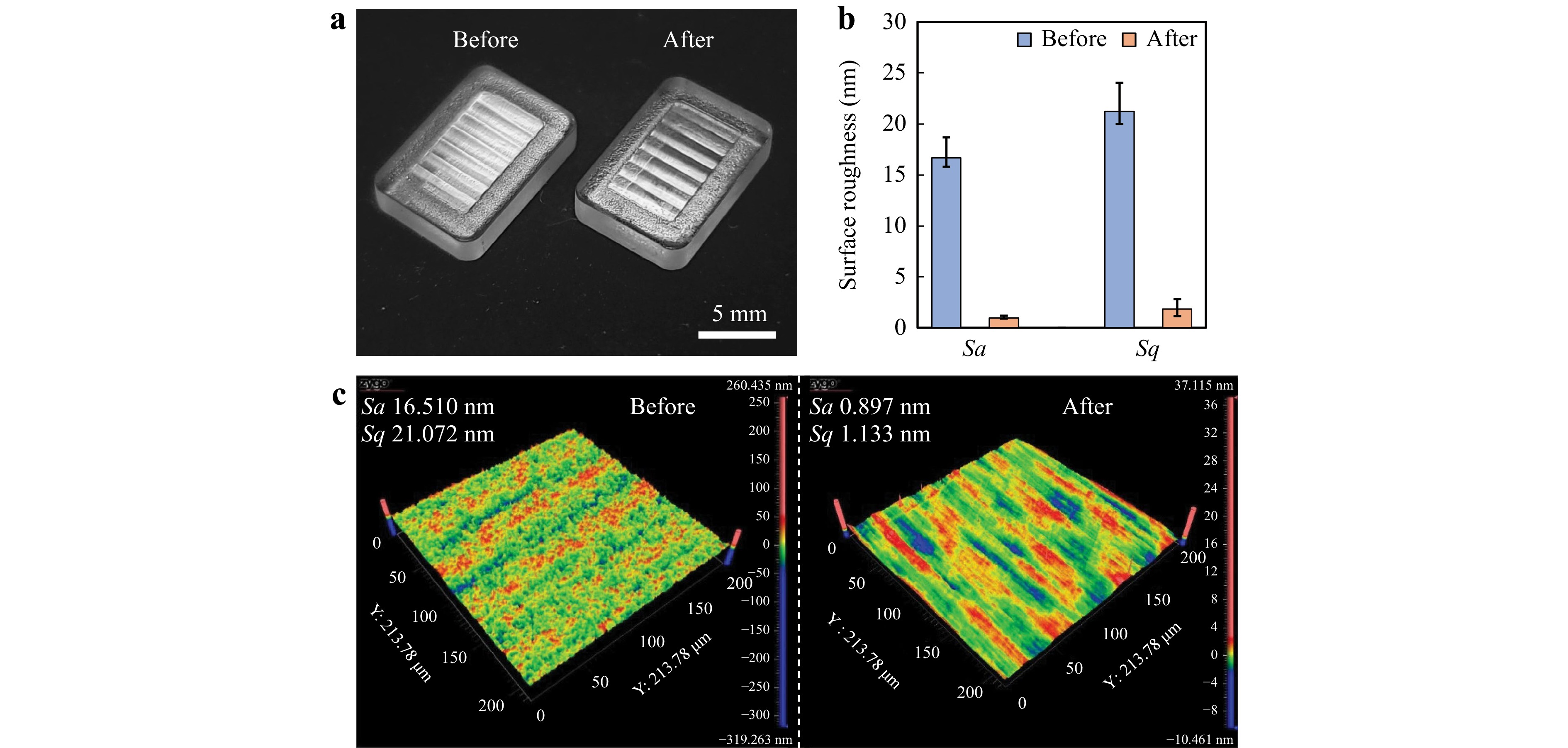
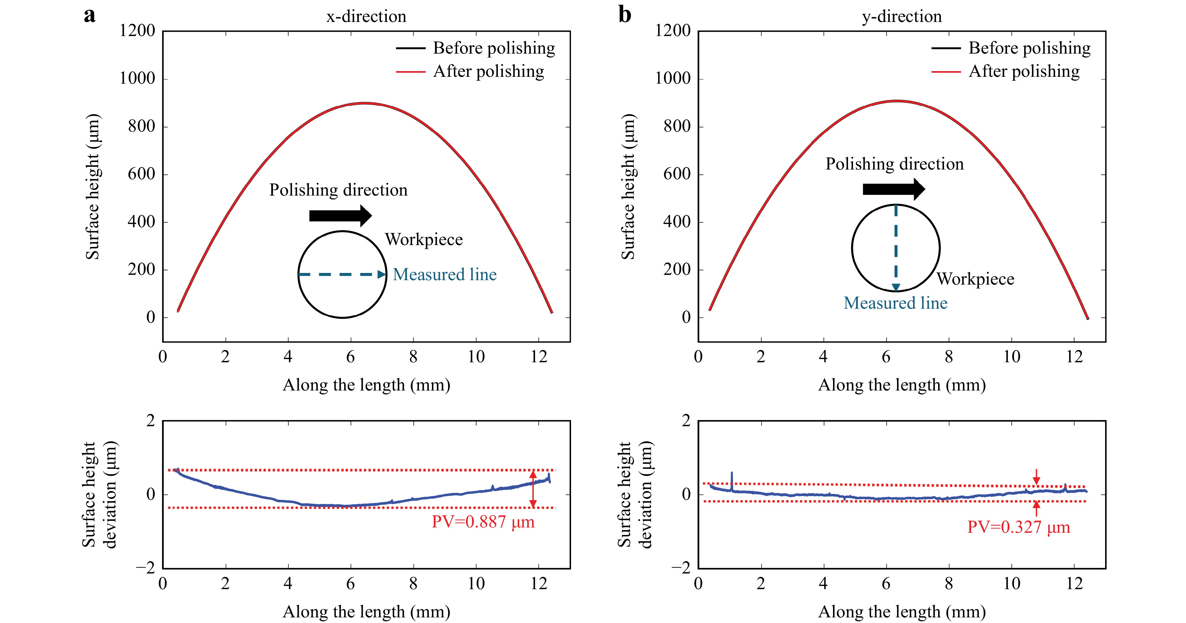
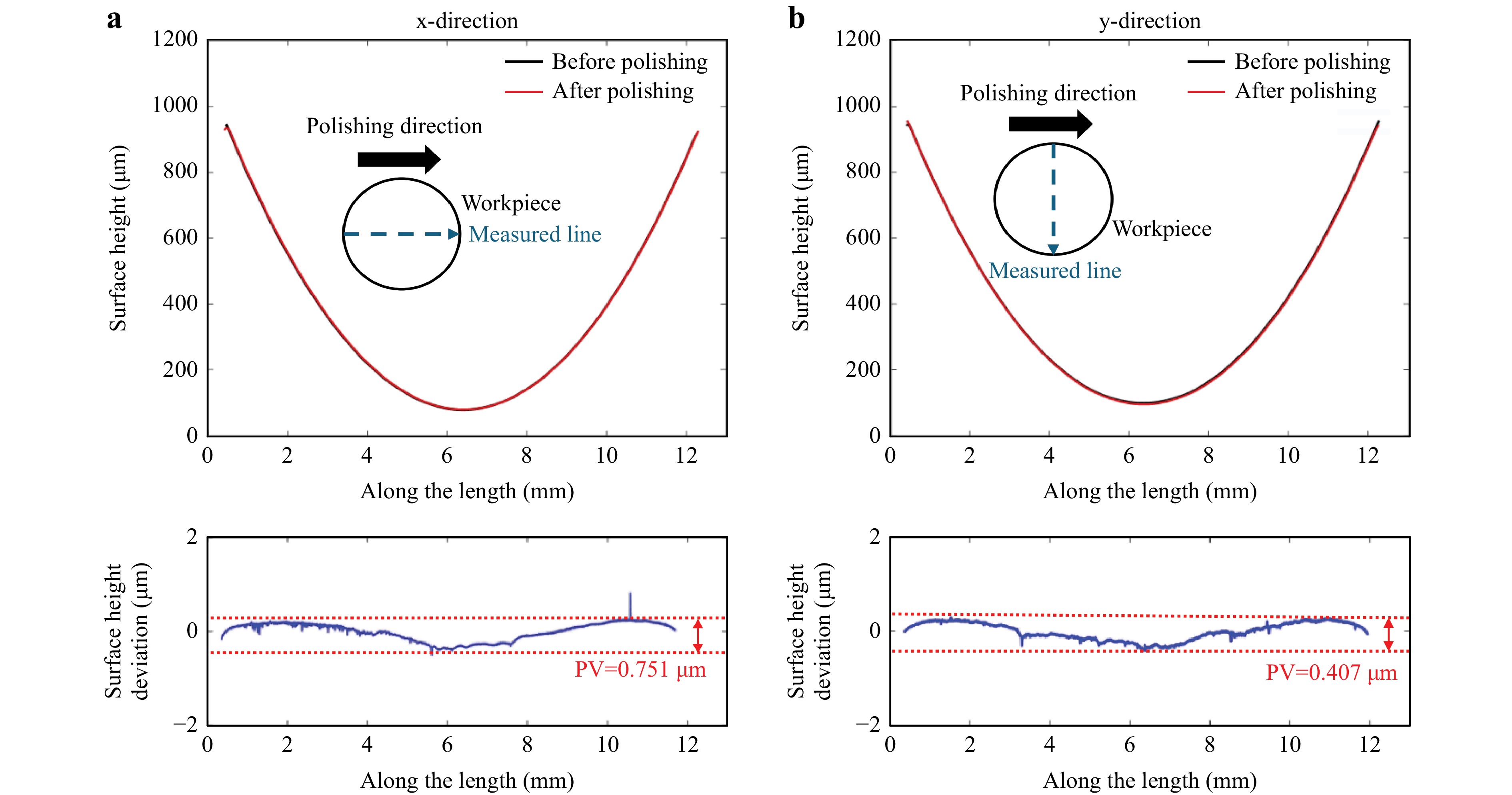
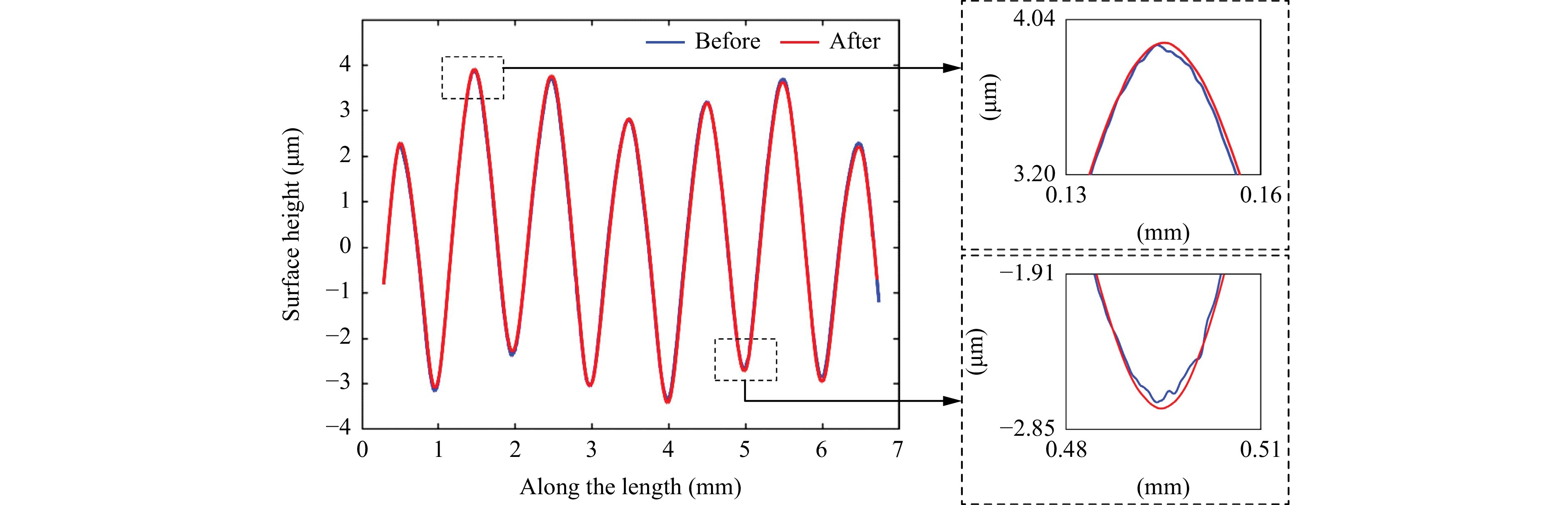
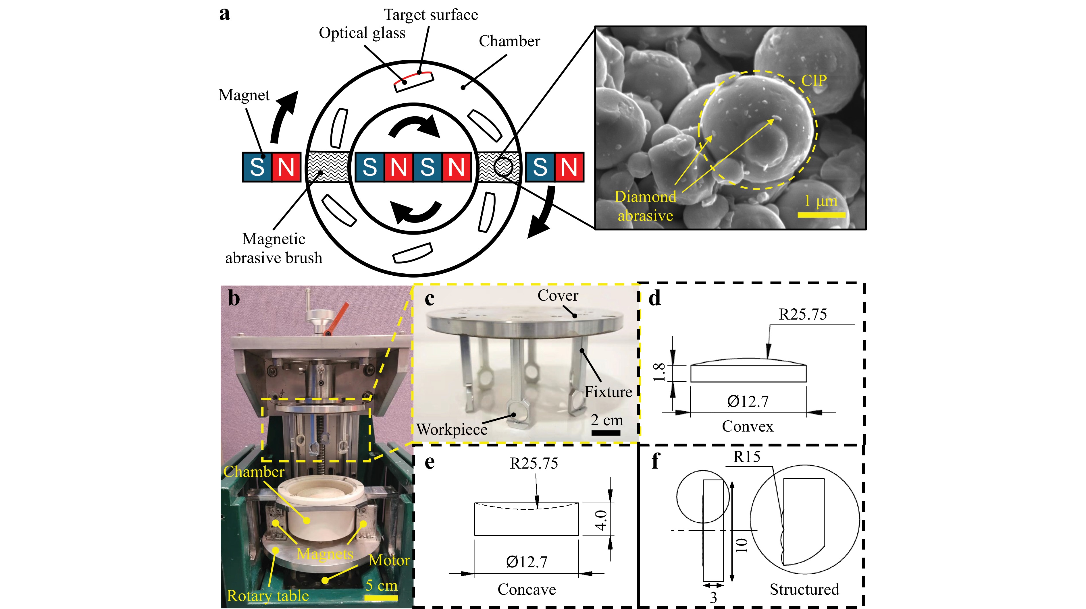
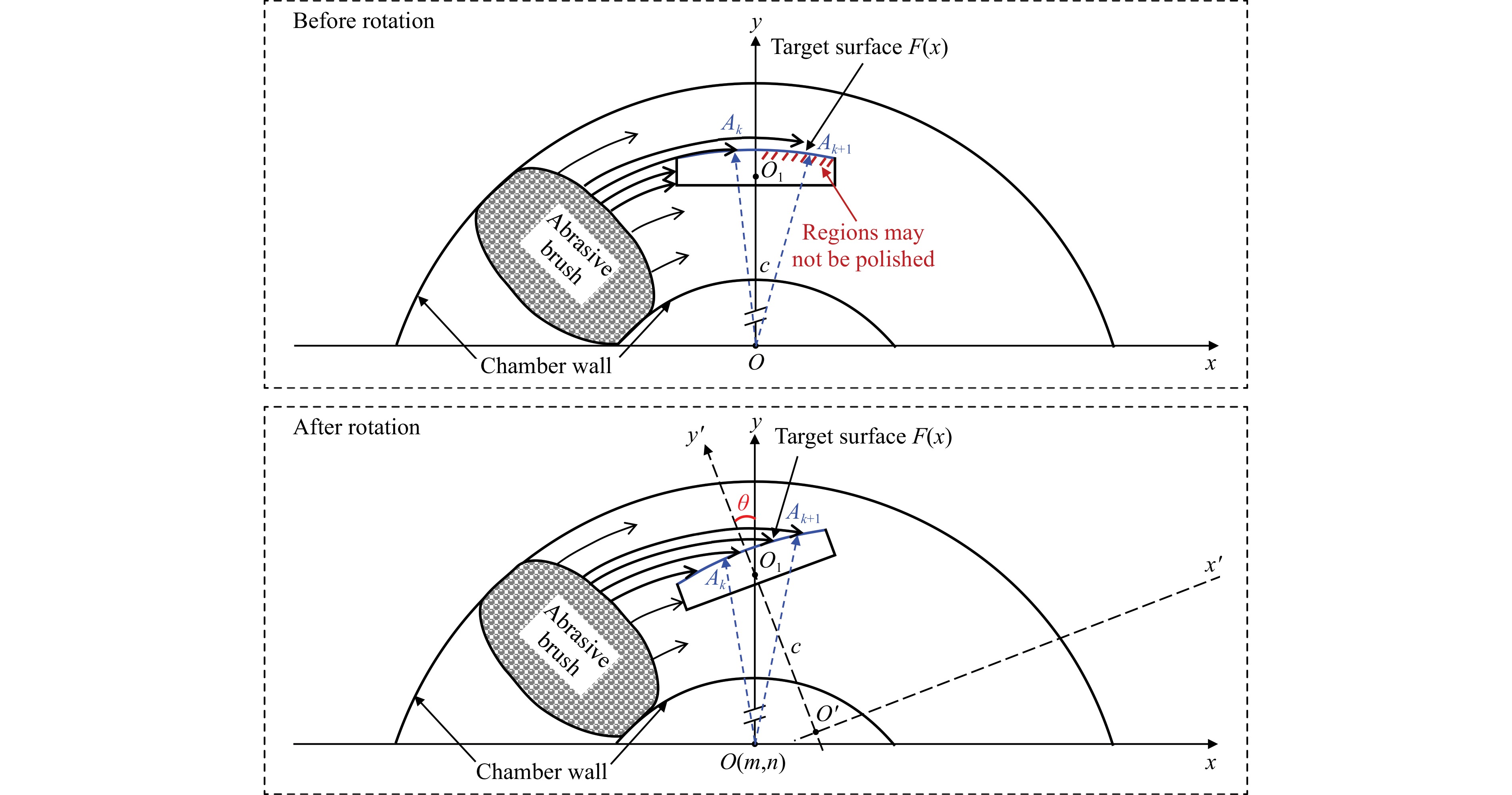
The demand for optical glass has been rapidly increasing in various industries, where an ultra-smooth surface and form accuracy are critical for the functional elements of the applications. To meet the high surface-quality requirements, a polishing process is usually adopted to finish the optical glass surface to ensure an ultra-smooth surface and eliminate sub-surface damage. However, current ultra-precision polishing processes normally polish workpieces individually, leading to a low production efficiency and high polishing costs. Current mass-finishing methods cannot be used for optical glasses. Therefore, magnetic-field-assisted batch polishing (MABP) was proposed in this study to overcome this research gap and provide an efficient and cost-effective method for industrial use. A series of polishing experiments were conducted on typical optical components under different polishing parameters to evaluate the polishing performance of MABP on optical glasses. The results demonstrated that MABP is an efficient method to simultaneously polish multiple lenses while achieving a surface roughness, indicated by the arithmetic mean height (Sa), of 0.7 nm and maintained a sub-micrometer surface form for all the workpieces. In addition, no apparent sub-surface damage was observed, indicating the significant potential for the high-quality rapid polishing of optical glasses. The proposed method is highly competitive compared to the current optical polishing methods, which has the potential to revolutionize the polishing process for small optics.
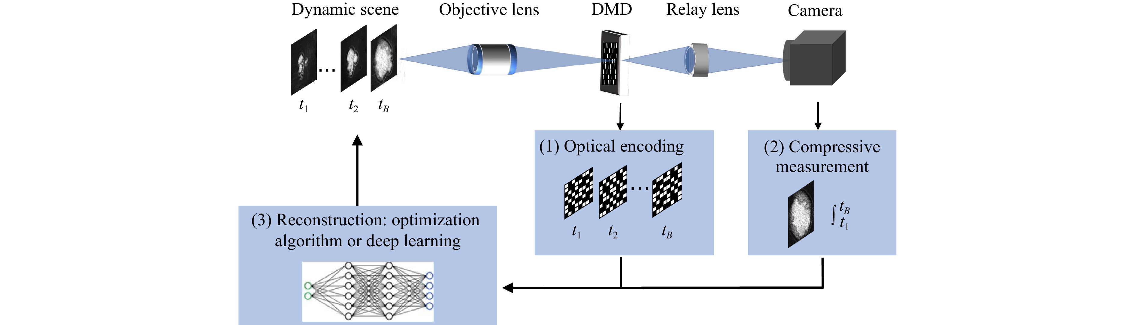
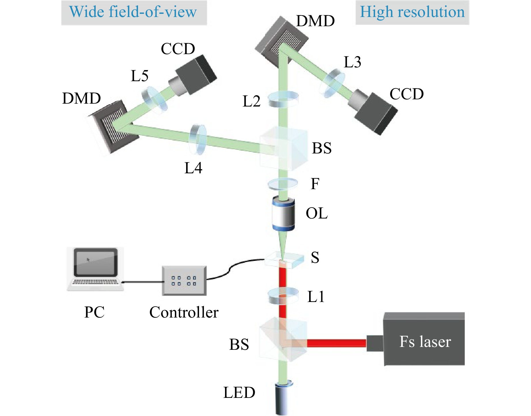
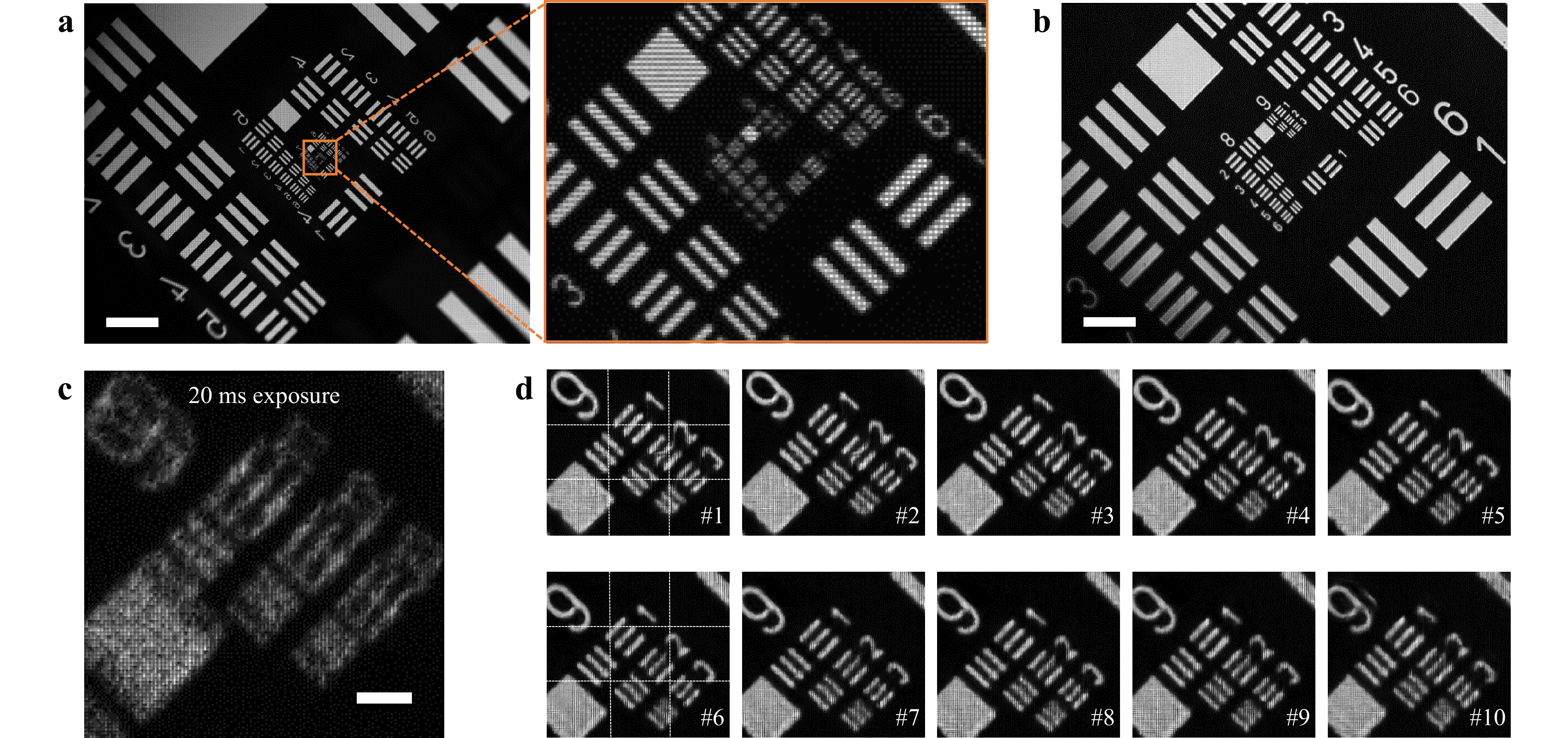
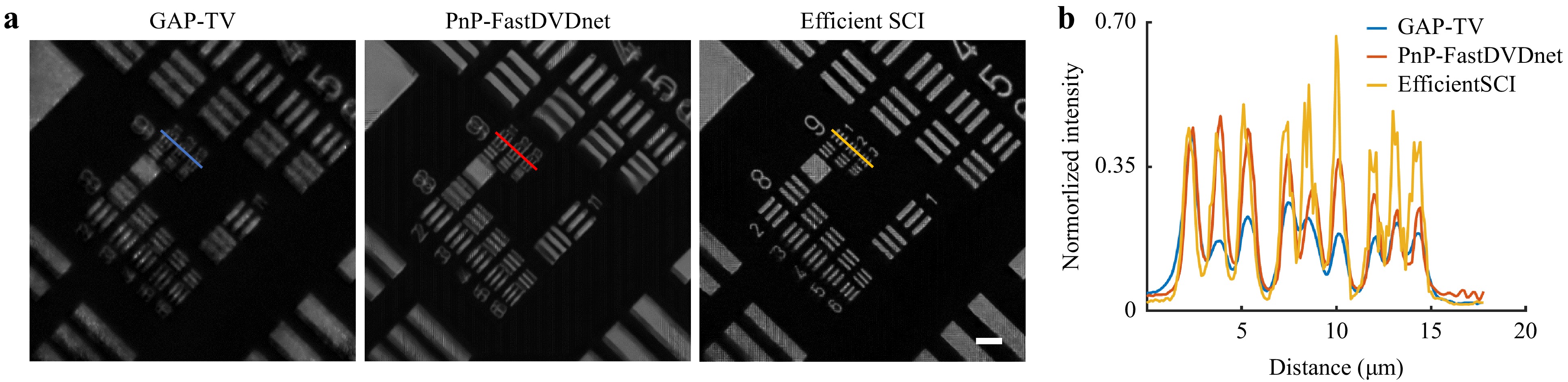
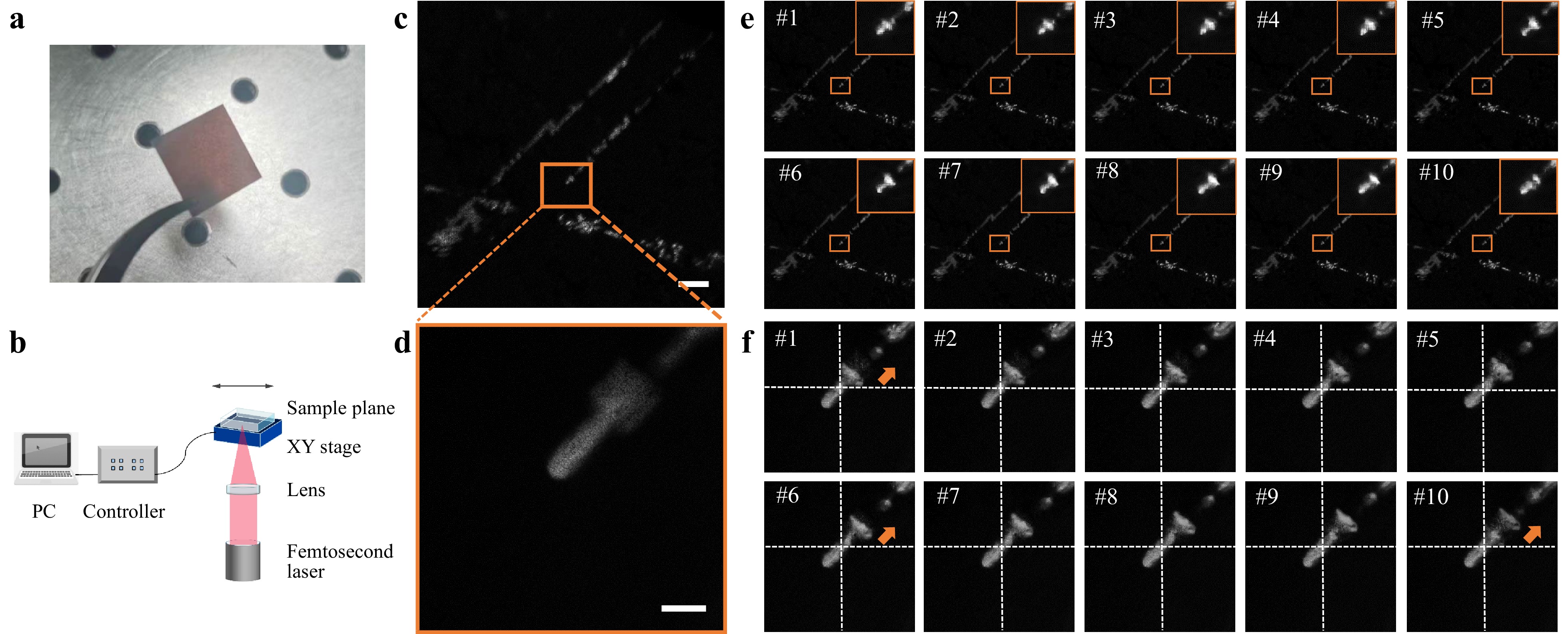
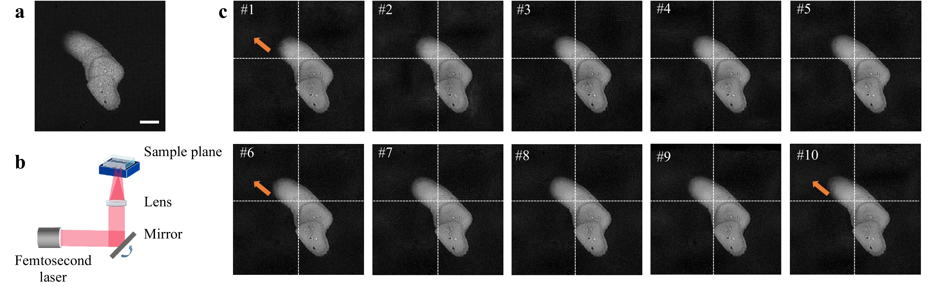
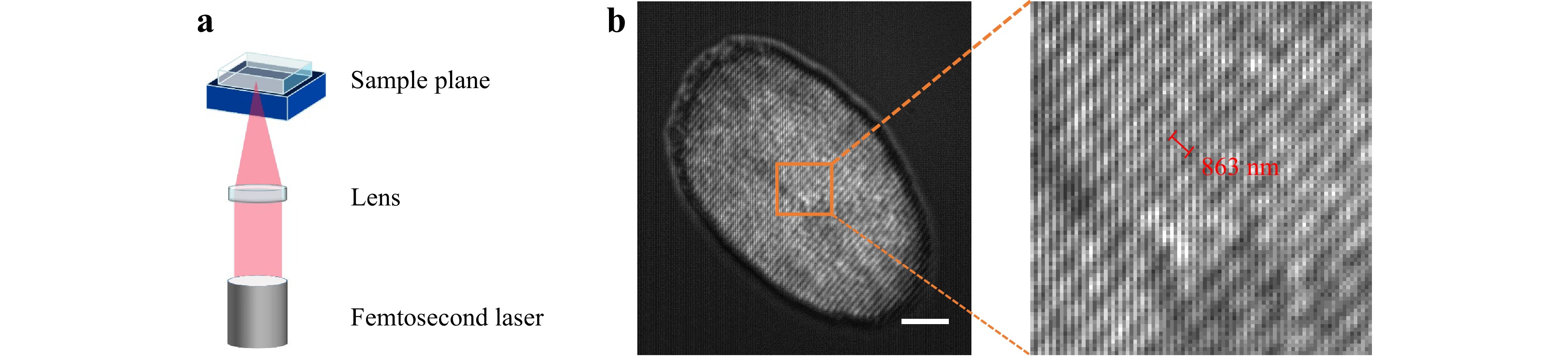
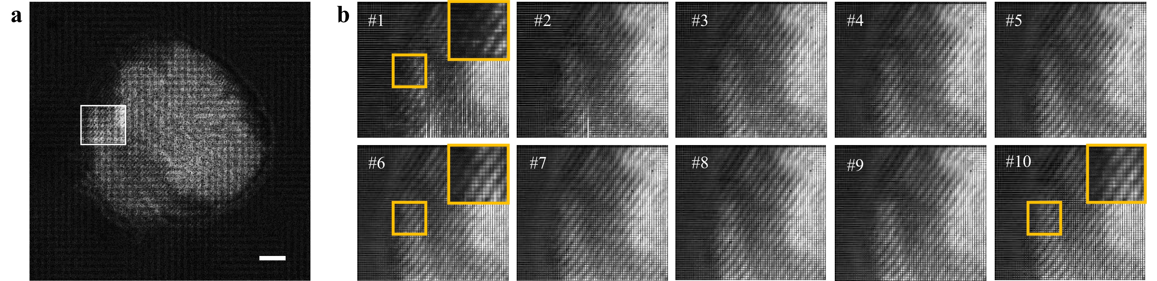
Over the last few decades, ultrafast laser processing has become a widely used tool for manufacturing microstructures and nanostructures. The real-time monitoring of laser material processing provides opportunities to inspect processes and provide feedback. To date, in-situ and real-time monitoring of laser material processing has rarely been performed. To this end, we propose dual-path snapshot compressive microscopy (DP-SCM) for high-speed, large field-of-view, and high-resolution imaging for in-situ and real-time ultrafast laser processing. In the evaluation of DP-SCM, the field of view, lateral resolution, and imaging speed were measured to be 2 mm, 775 nm, and 500 fps, respectively. In ultrafast laser processing, the laser scanning process is observed using a DP-SCM system when translating the sample stage and scanning the focused femtosecond laser. Finally, we monitored the development of a self-organized nanograting structure to validate the potential of our system for unveiling new material mechanisms. The proposed method serves as an add-up (plug-and-play) module for any imaging setup and has vast potential for opening new avenues for high-throughput imaging in laser material processing.
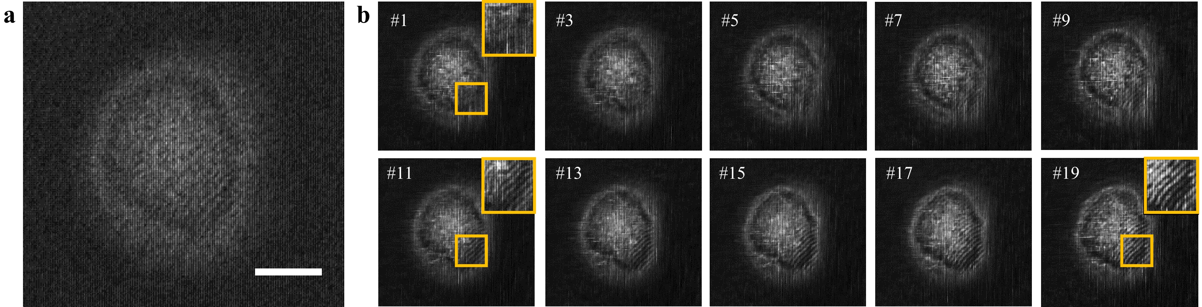
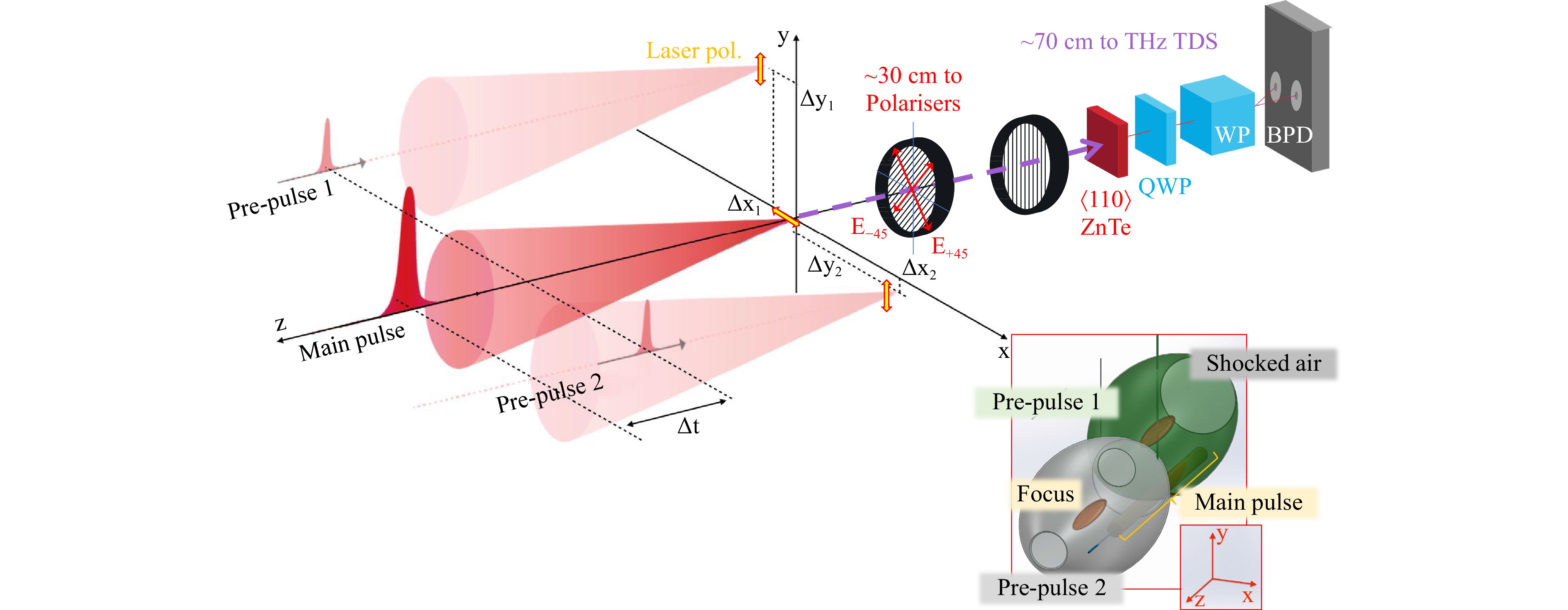
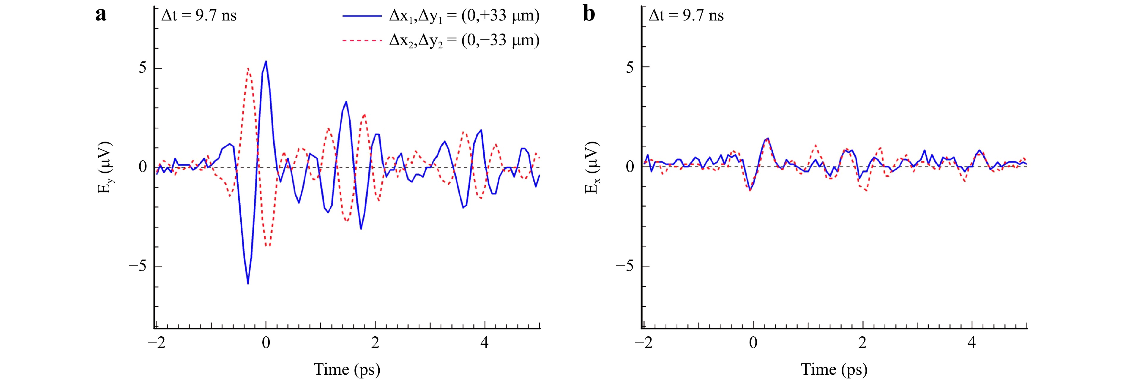
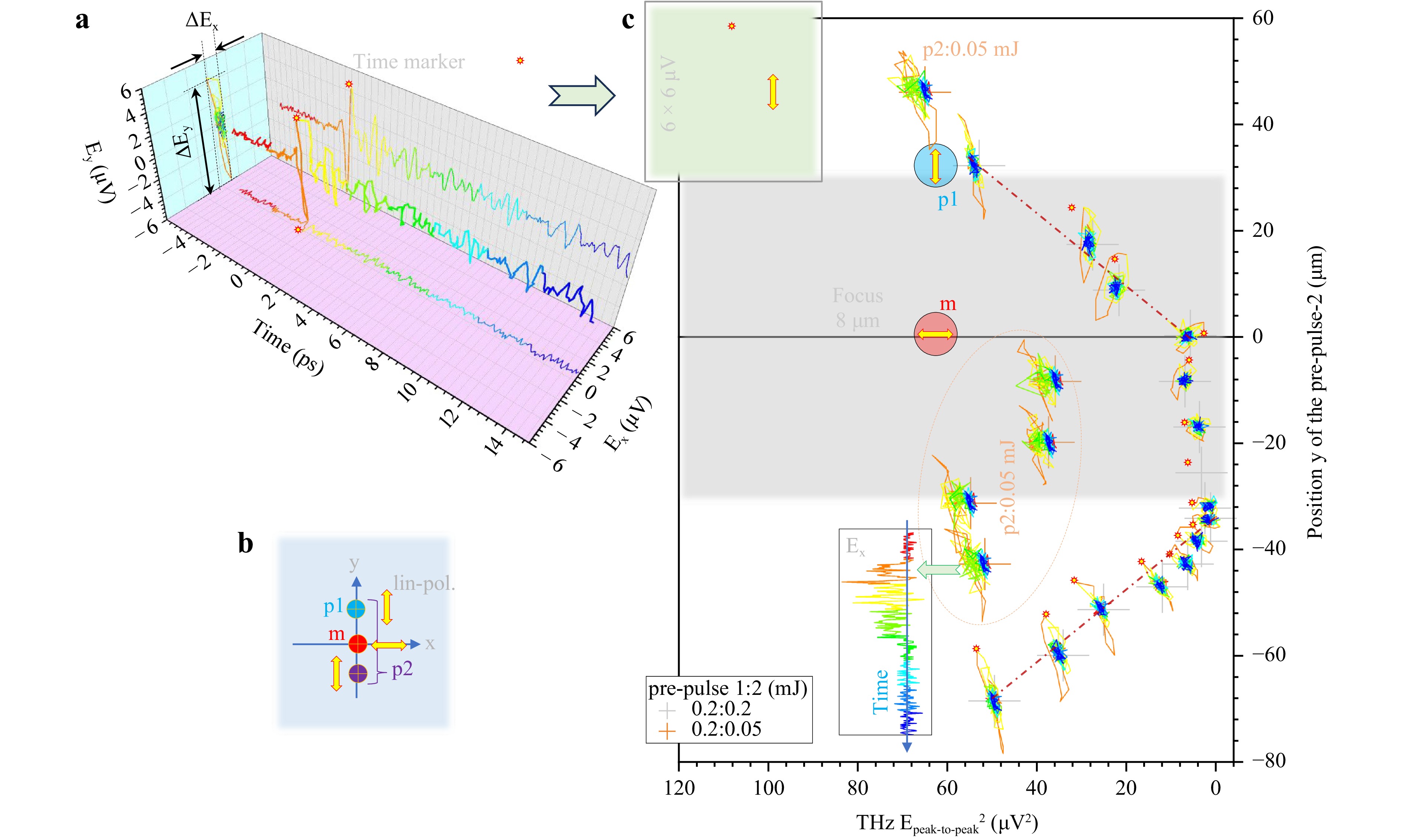
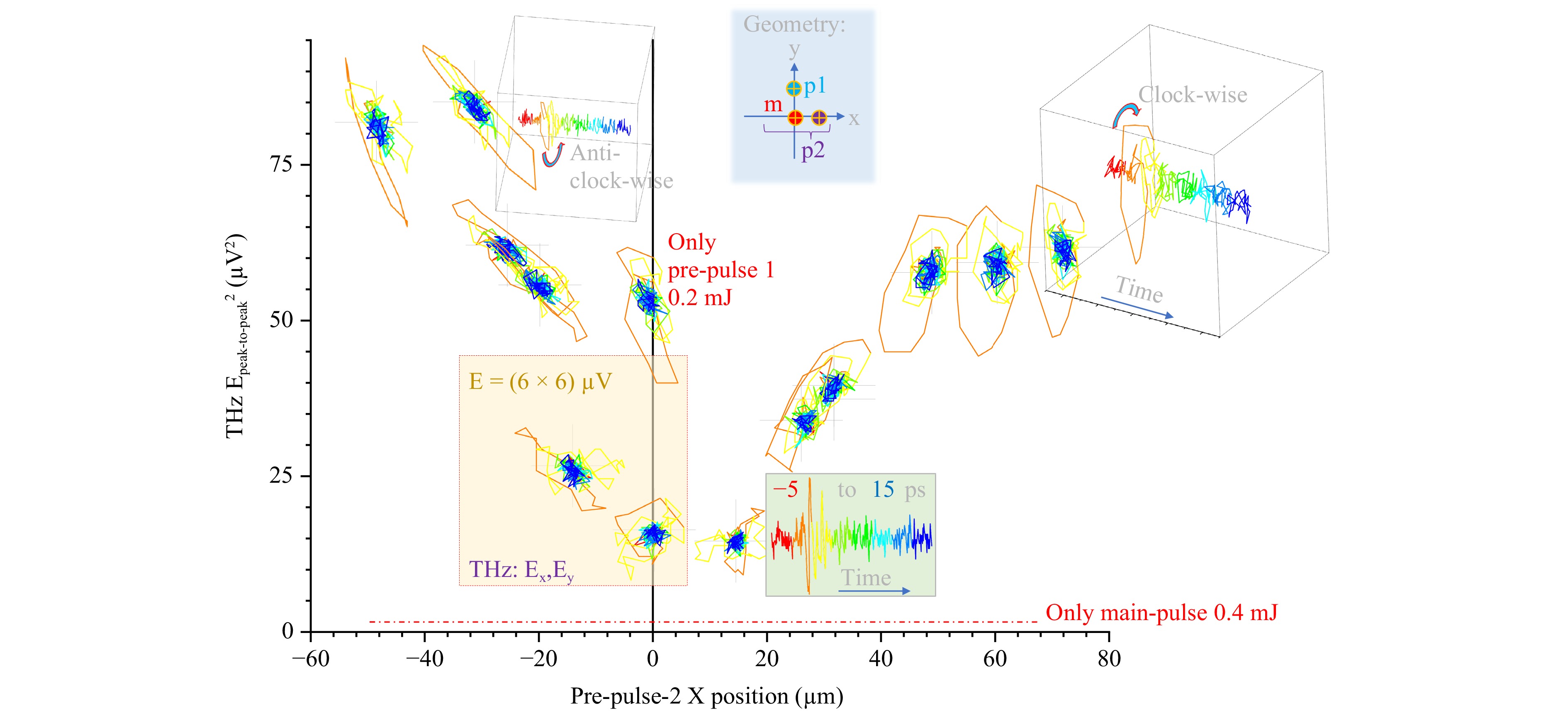
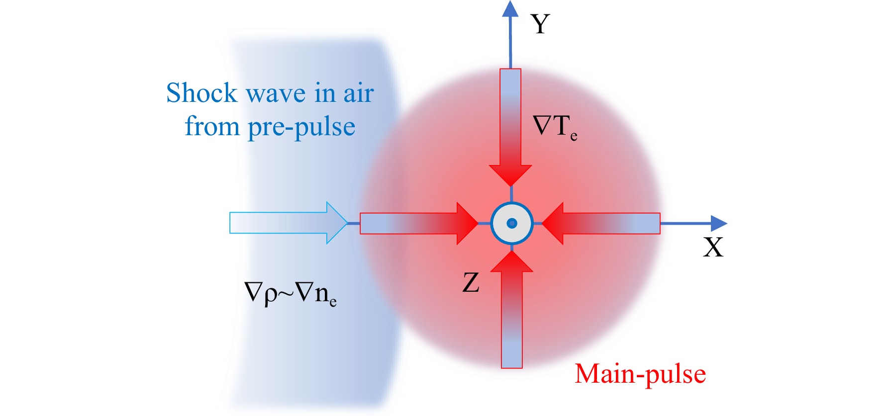
Emission of THz radiation from air breakdown at focused ultra-short fs-laser pulses (800 nm/35 fs) was investigated for the 3D spatio-temporal control where two pre-pulses are used before the main-pulse. The laser pulse induced air breakdown forms a ~ 120 μm-long focal volume generate shockwaves which deliver a denser air into the focal region of the main pulse for enhanced generation of THz radiation at 0.1–2.5 THz spectral window. The intensity of pre- and main-pulses was at the tunnelling ionisation intensities (1–3) × 1016 W/cm2 and corresponded to sub-critical (transparent) plasma formation in air. Polarisation analysis of THz radiation revealed that orientation of the air density gradients generated by pre-pulses and their time-position locations defined the ellipticity of the generated THz electrical field. The rotational component of electric current is the origin of THz radiation.
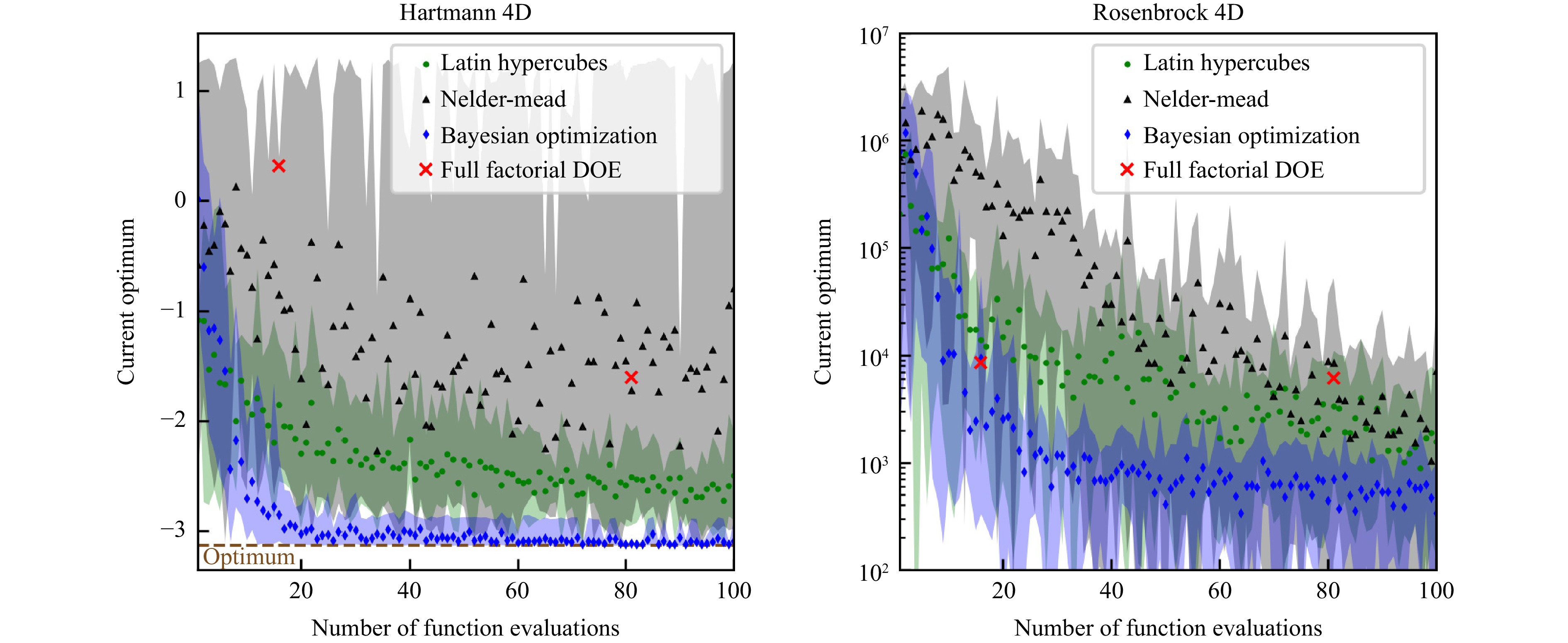
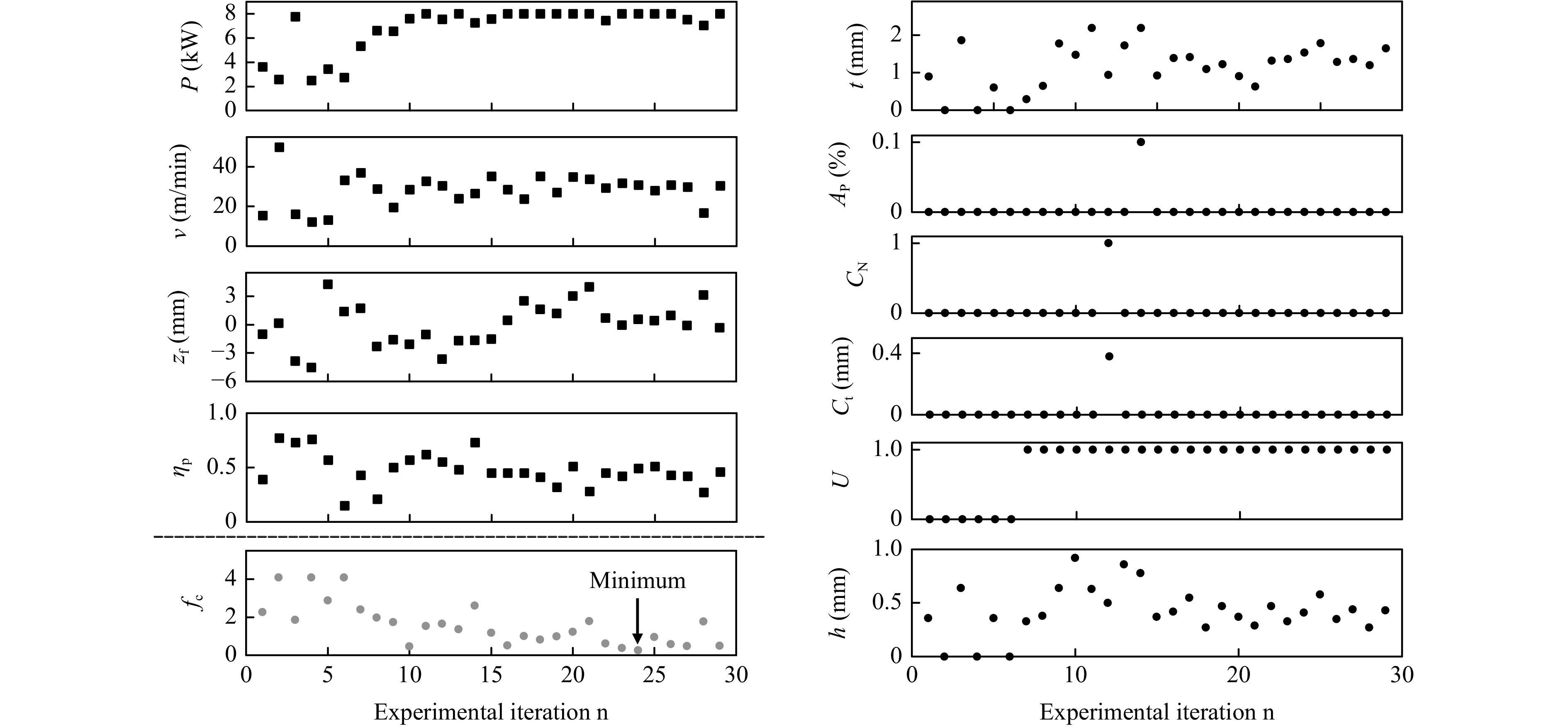
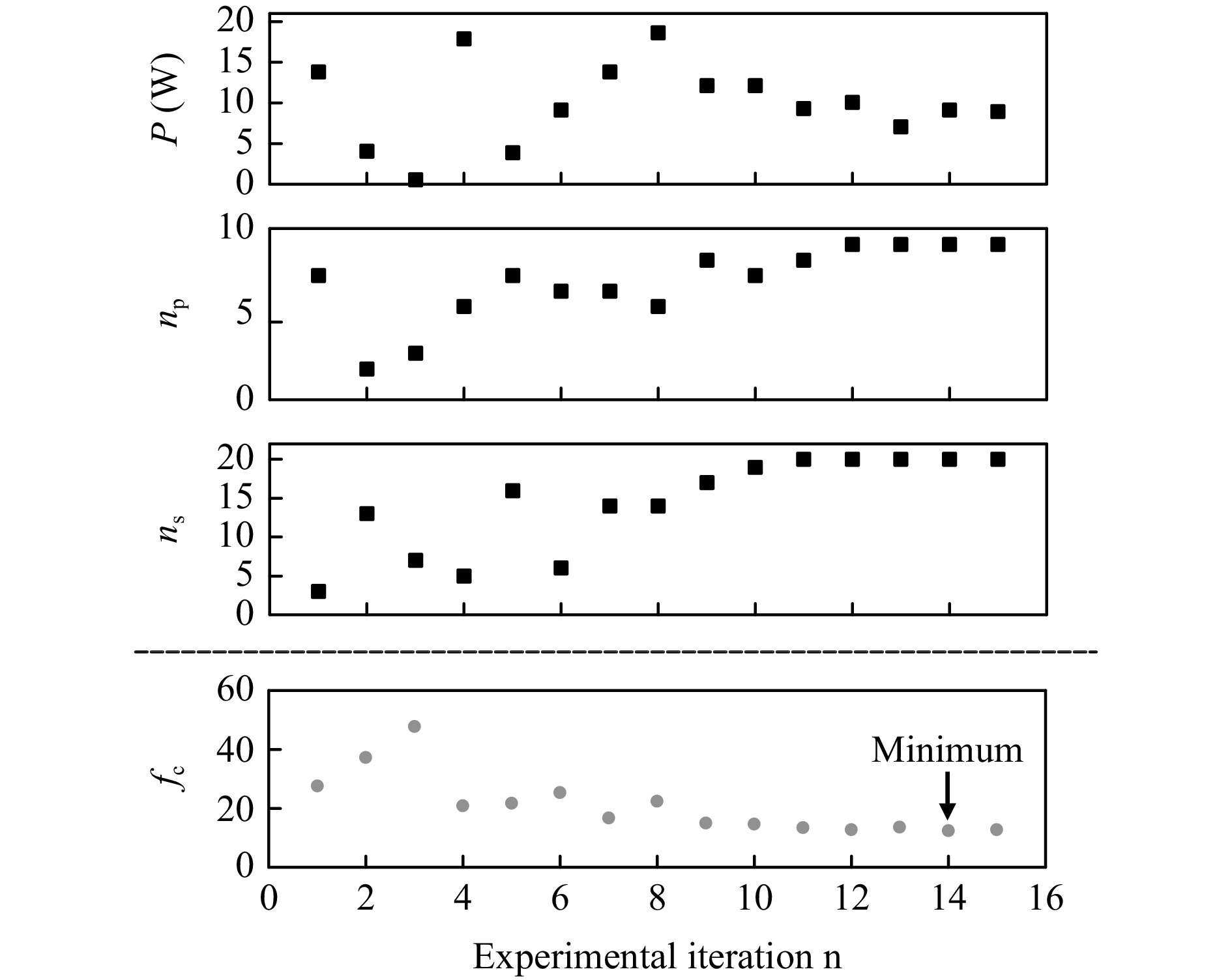
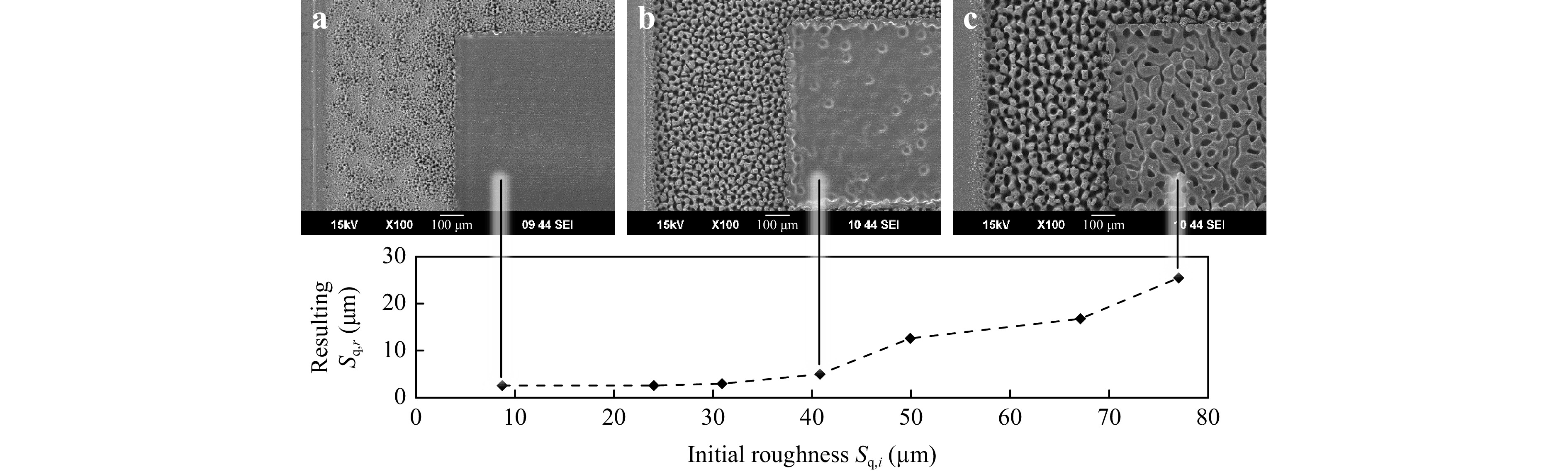
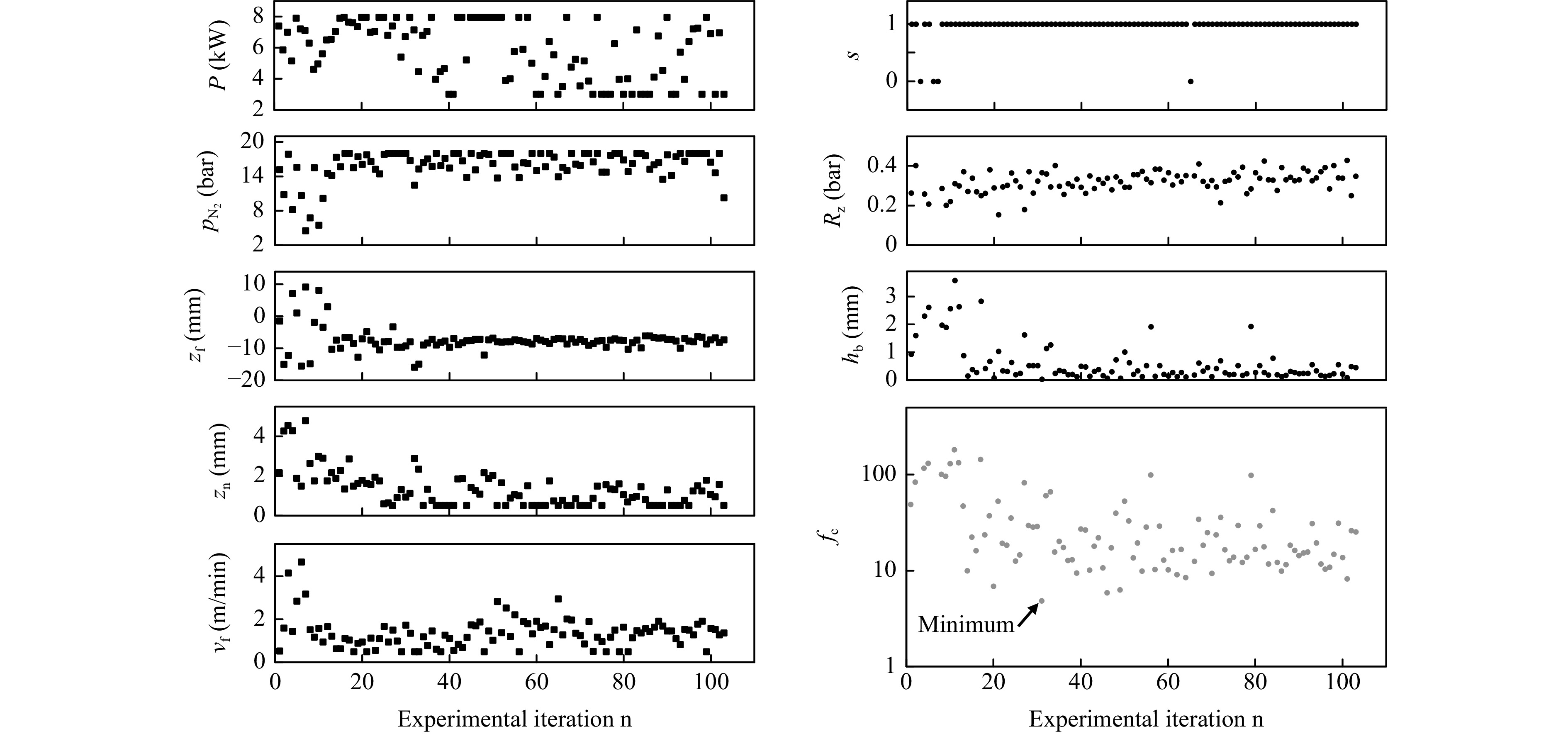
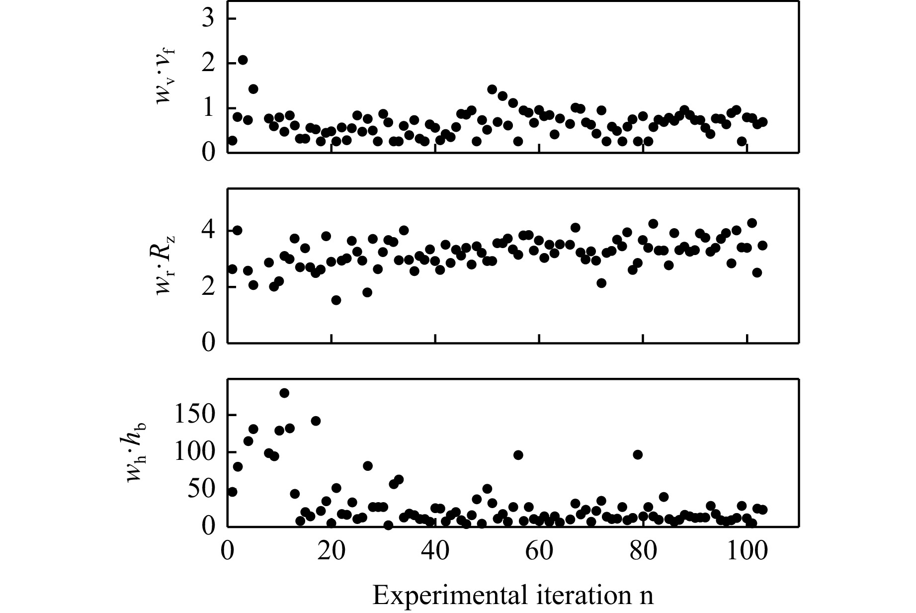
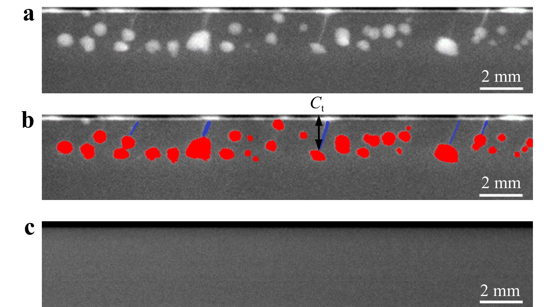
Optimizing laser processes is historically challenging, requiring extensive and costly experimentation. To solve this issue, we apply Bayesian optimization for process parameter optimization to laser cutting, welding, and polishing. We demonstrate how readily available Bayesian optimization frameworks enable efficient optimization of laser processes with only modest expert knowledge. Case studies on laser cutting, welding, and polishing highlight its adaptability to real-world manufacturing scenarios. Moreover, the examples emphasize that with suitable cost functions and boundaries an acceptable optimization result can be achieved after a reasonable number of experiments.
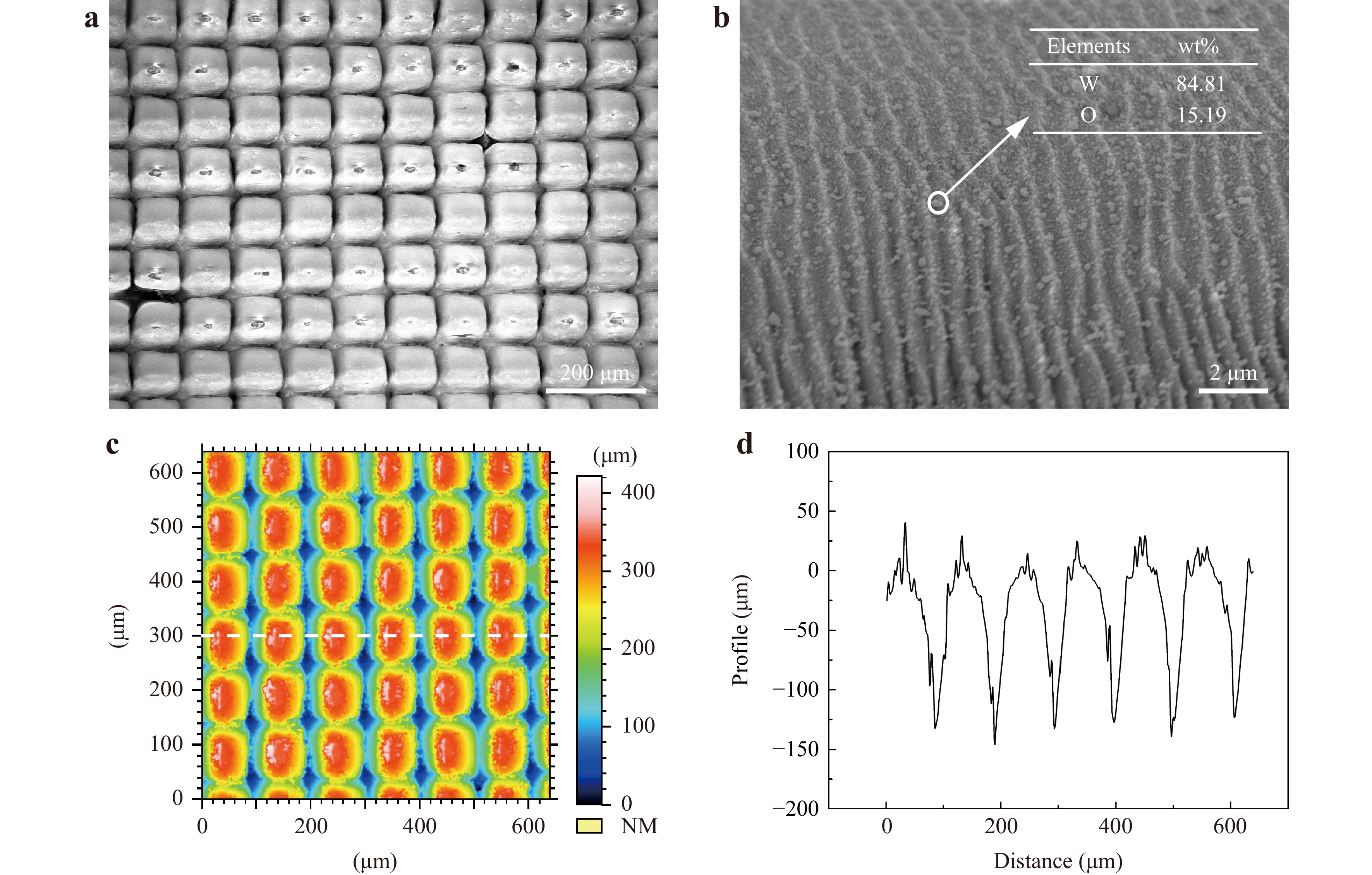
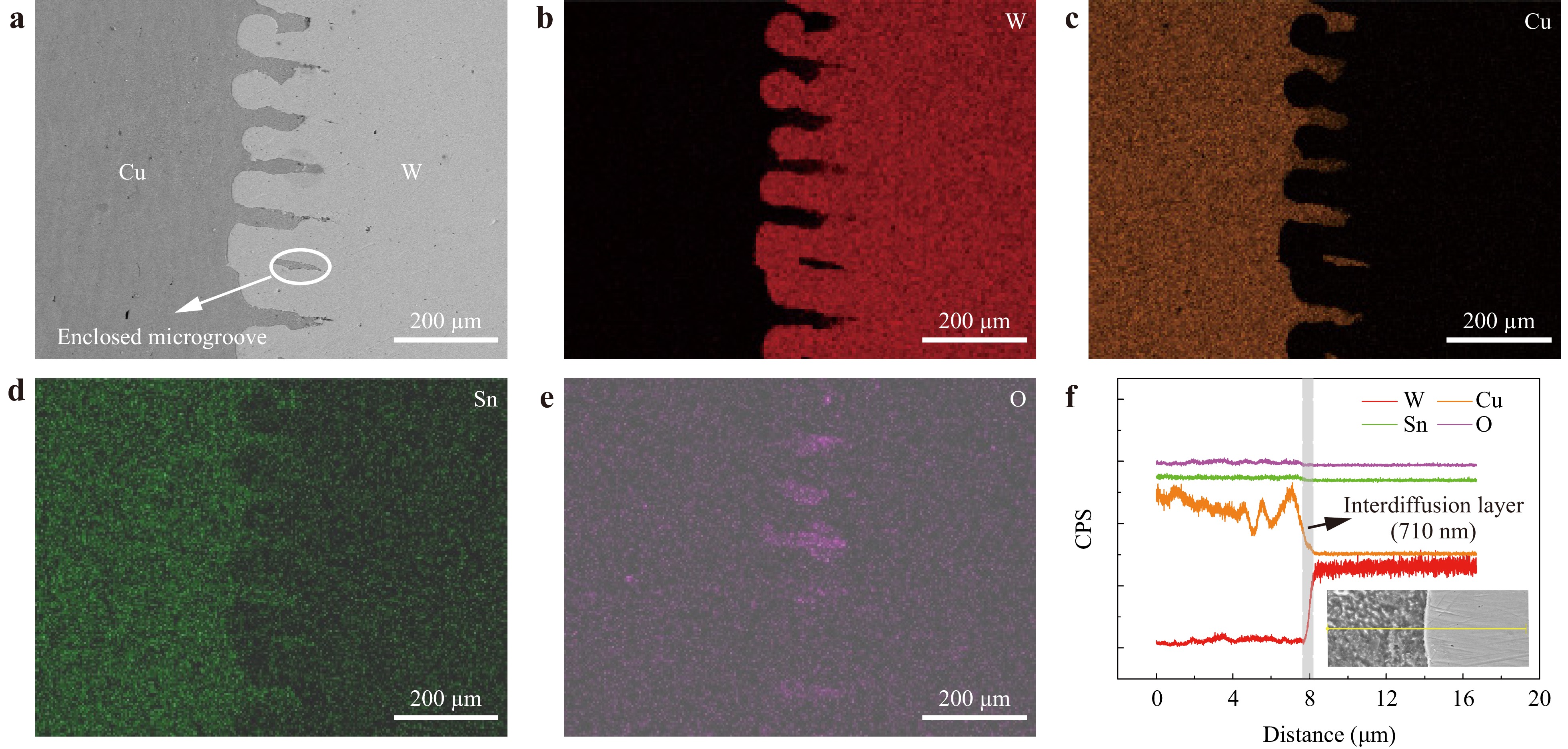
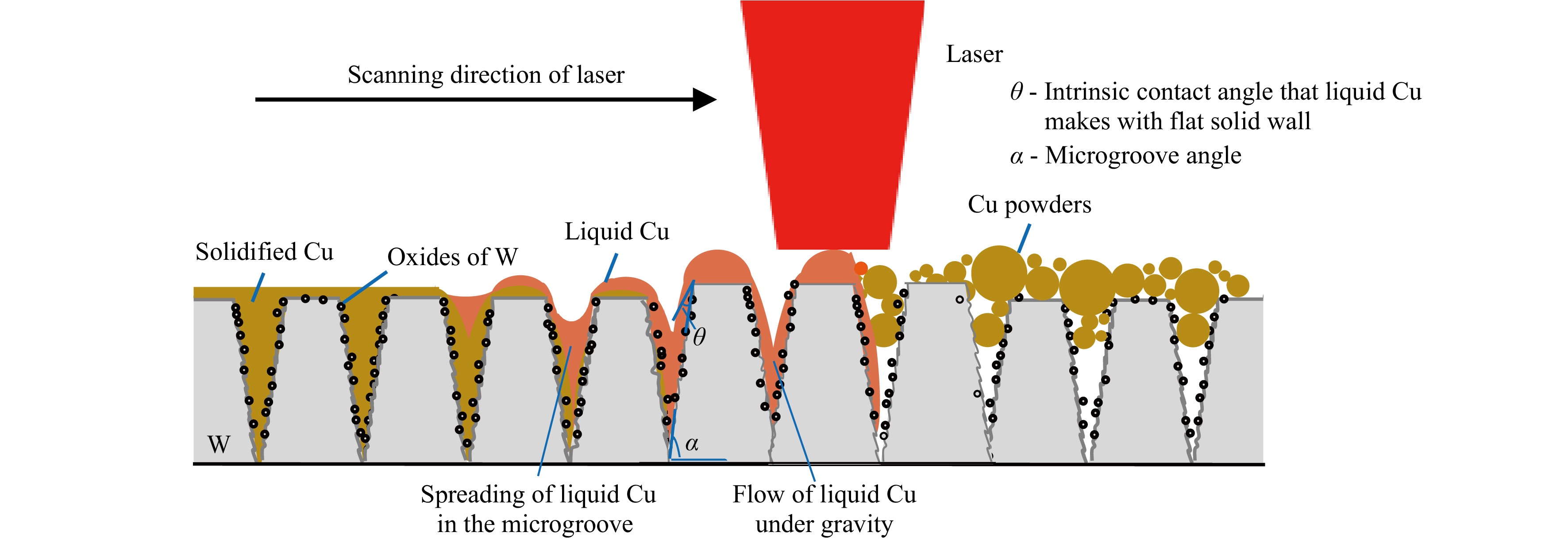
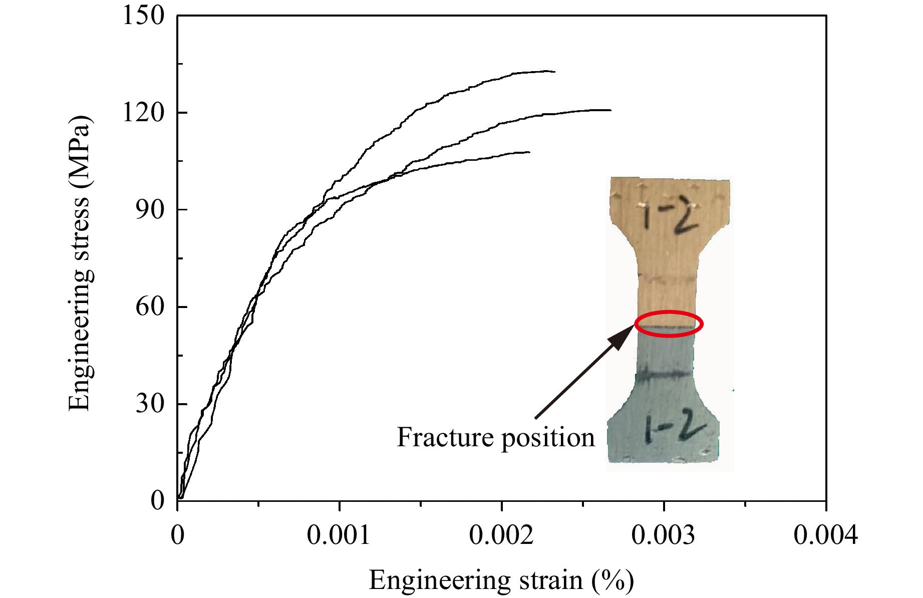
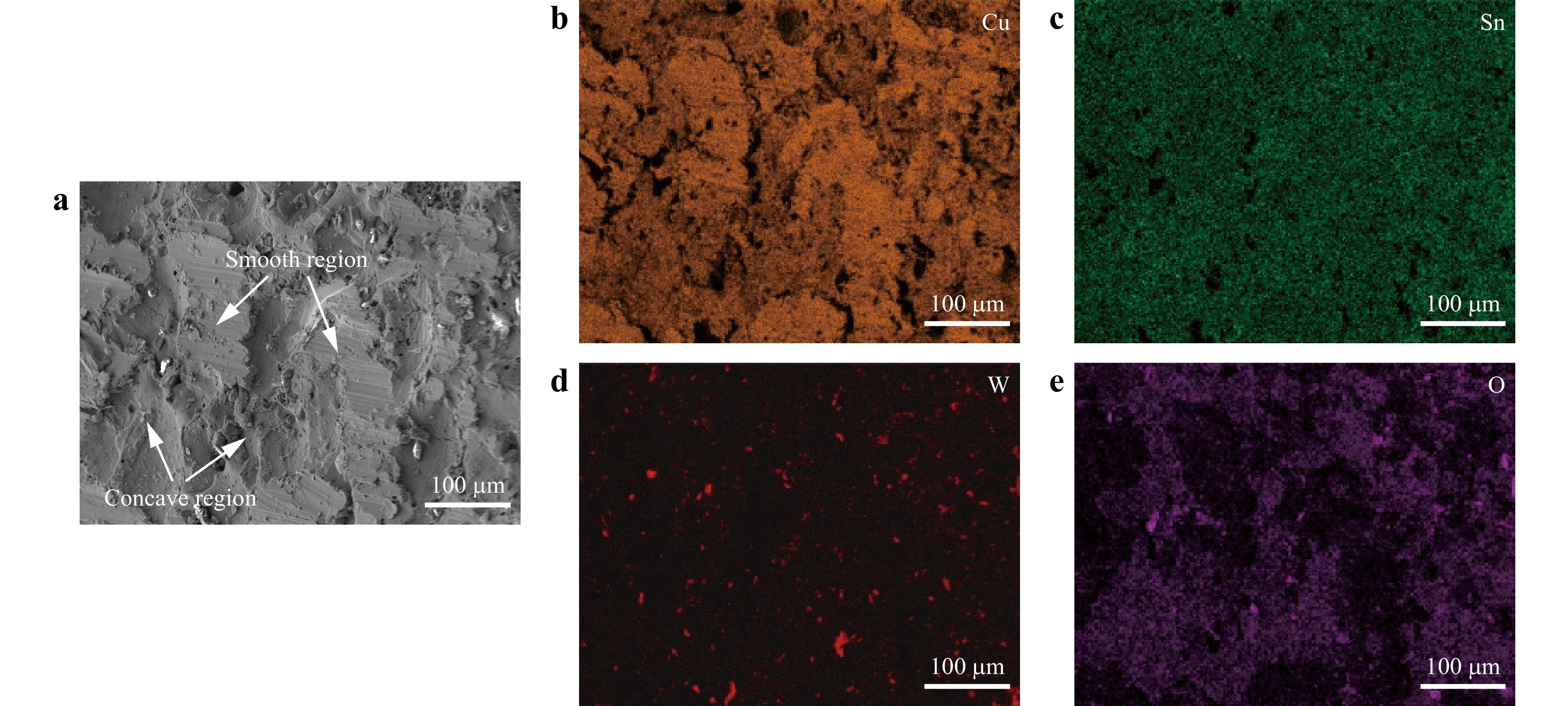
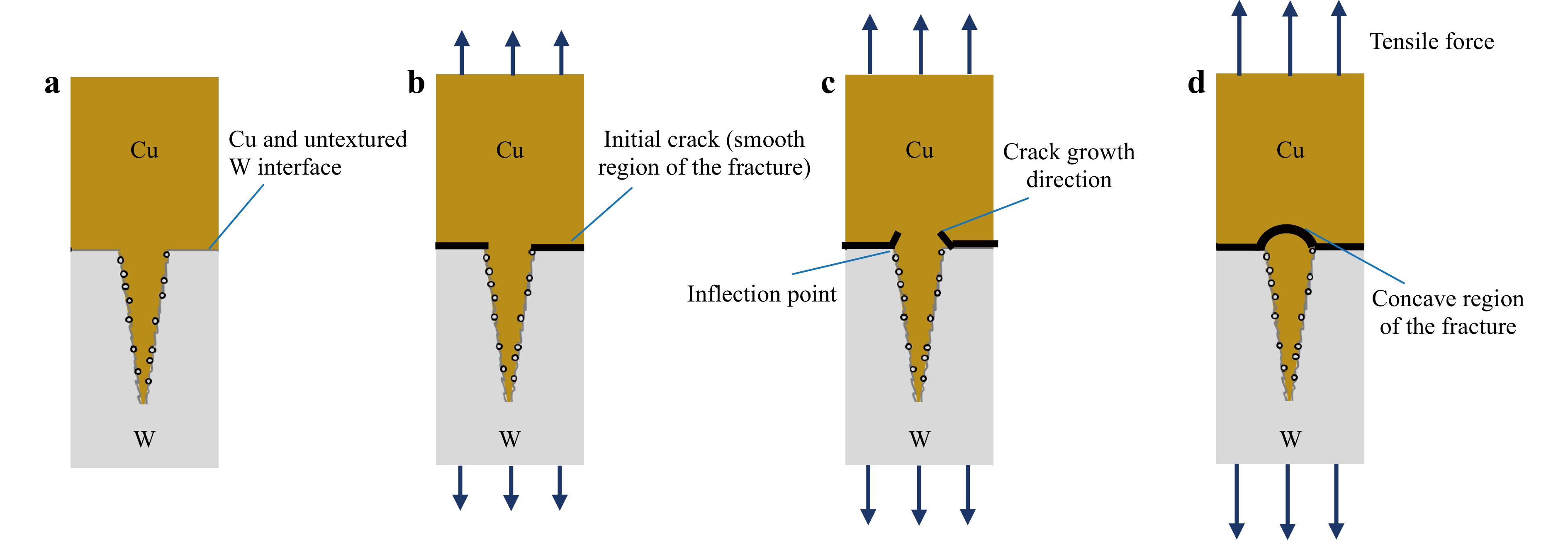
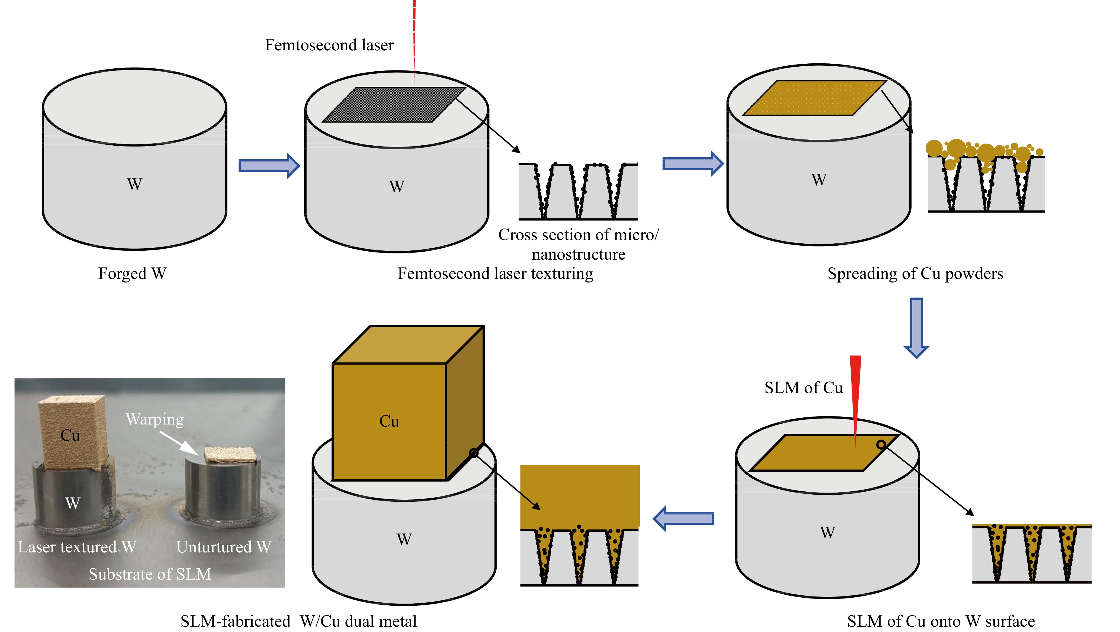
Selective laser melting (SLM) is a promising technology for fabricating complex components with W/Cu dual metal. To enhance the interfacial bonding of W/Cu dual metal, we propose a novel approach using laser texturing to fabricate micro/nanostructures on the W surface. The micro/nanostructures promoted the spreading of Cu in the liquid, inhibited defects, and considerably increased the contact area between W and Cu by mechanical interlocking. To the best of our knowledge, a W/Cu dual metal was successfully prepared by SLM without a transition layer the first time. The bonding strength of the two materials reached 123 MPa, close to that of a W/Cu dual metal joint prepared by diffusion bonding.
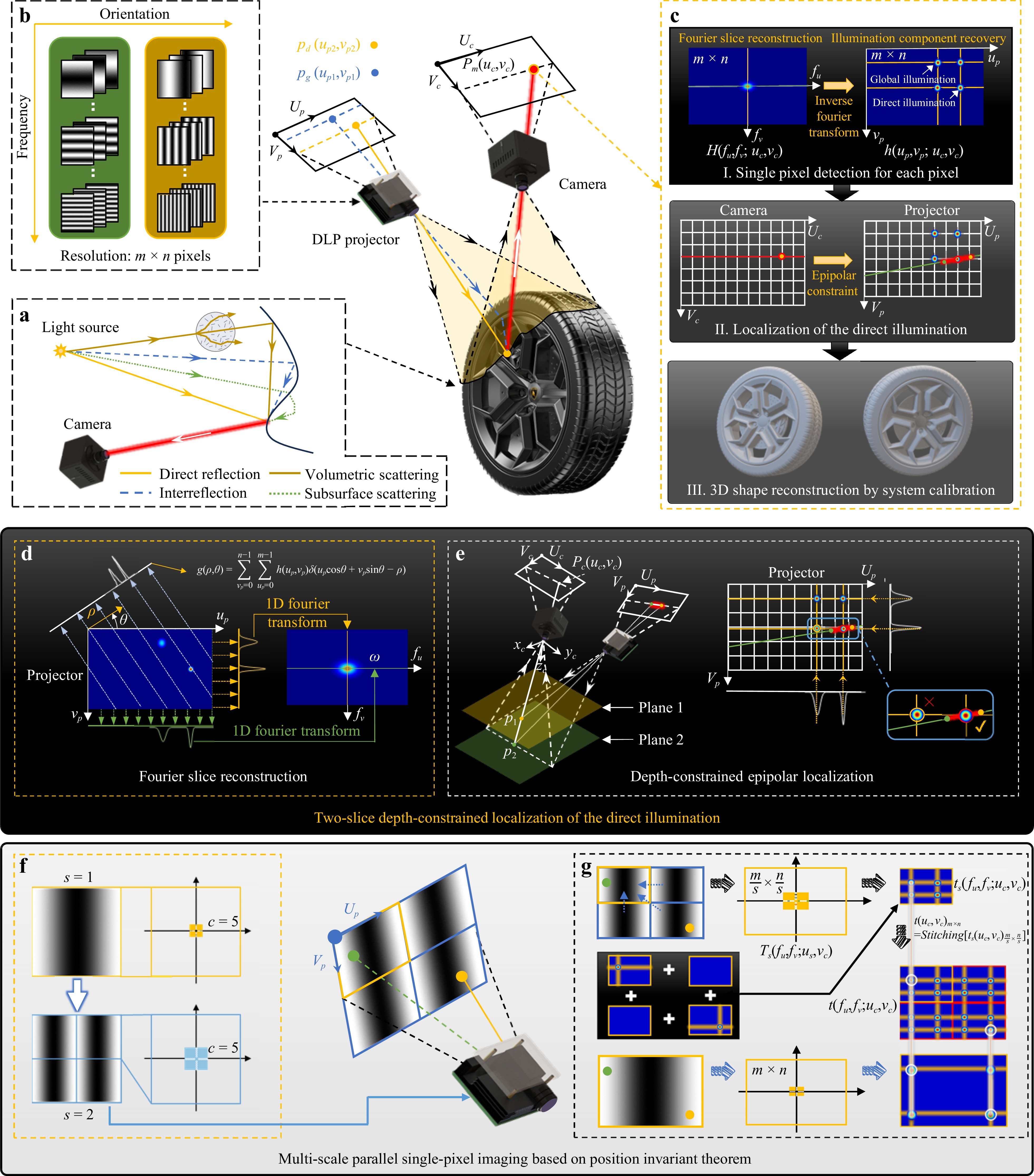
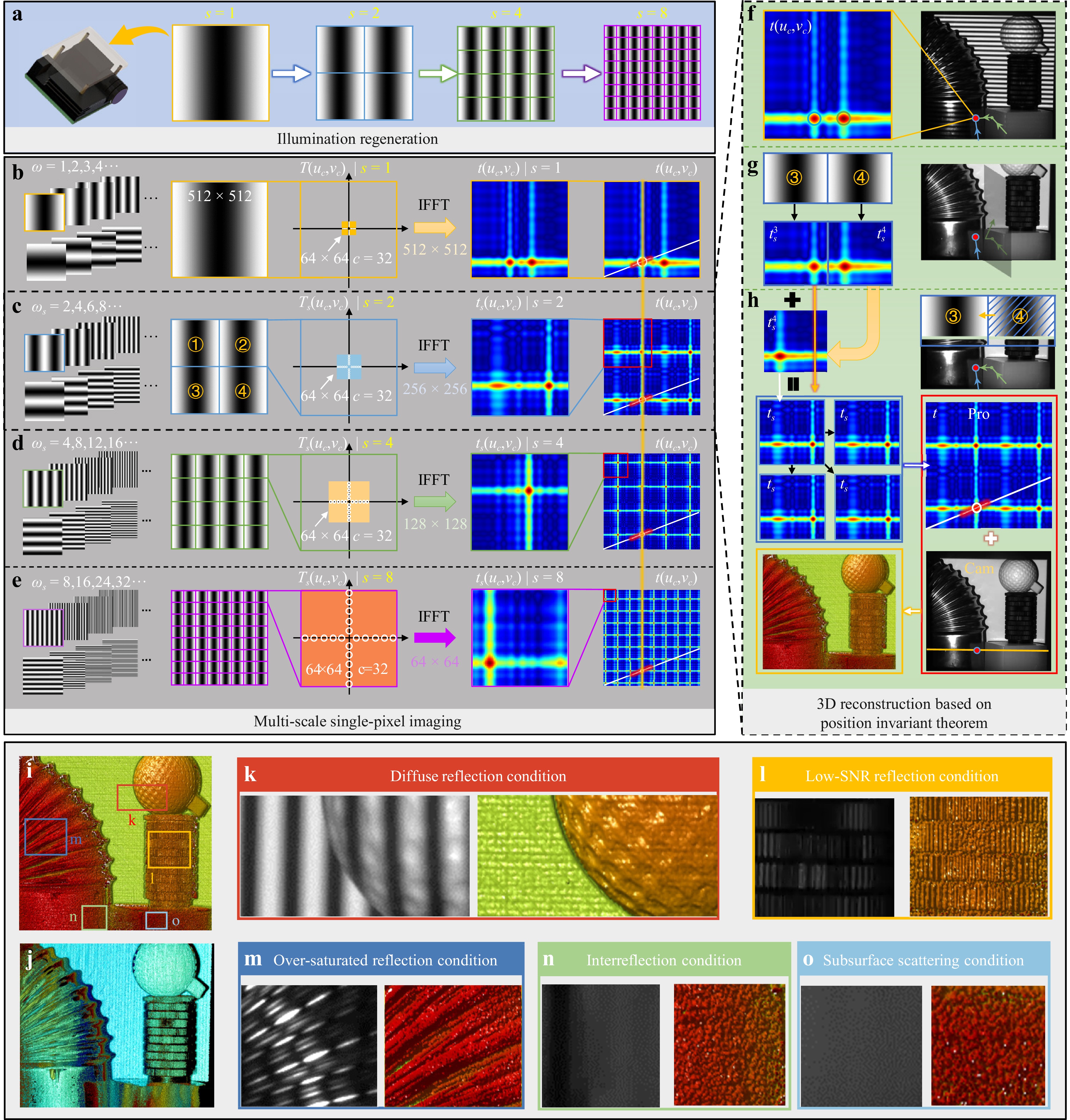
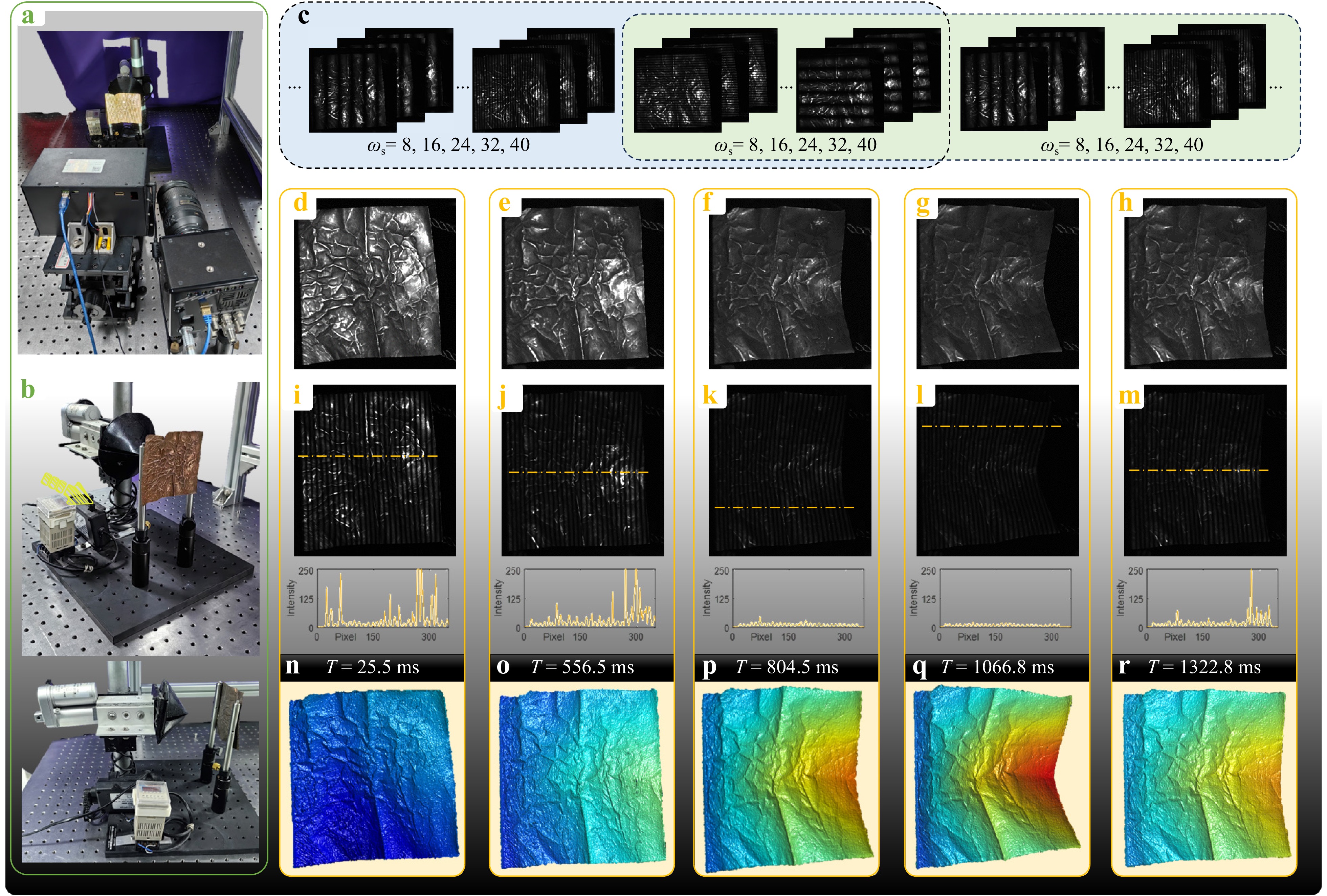
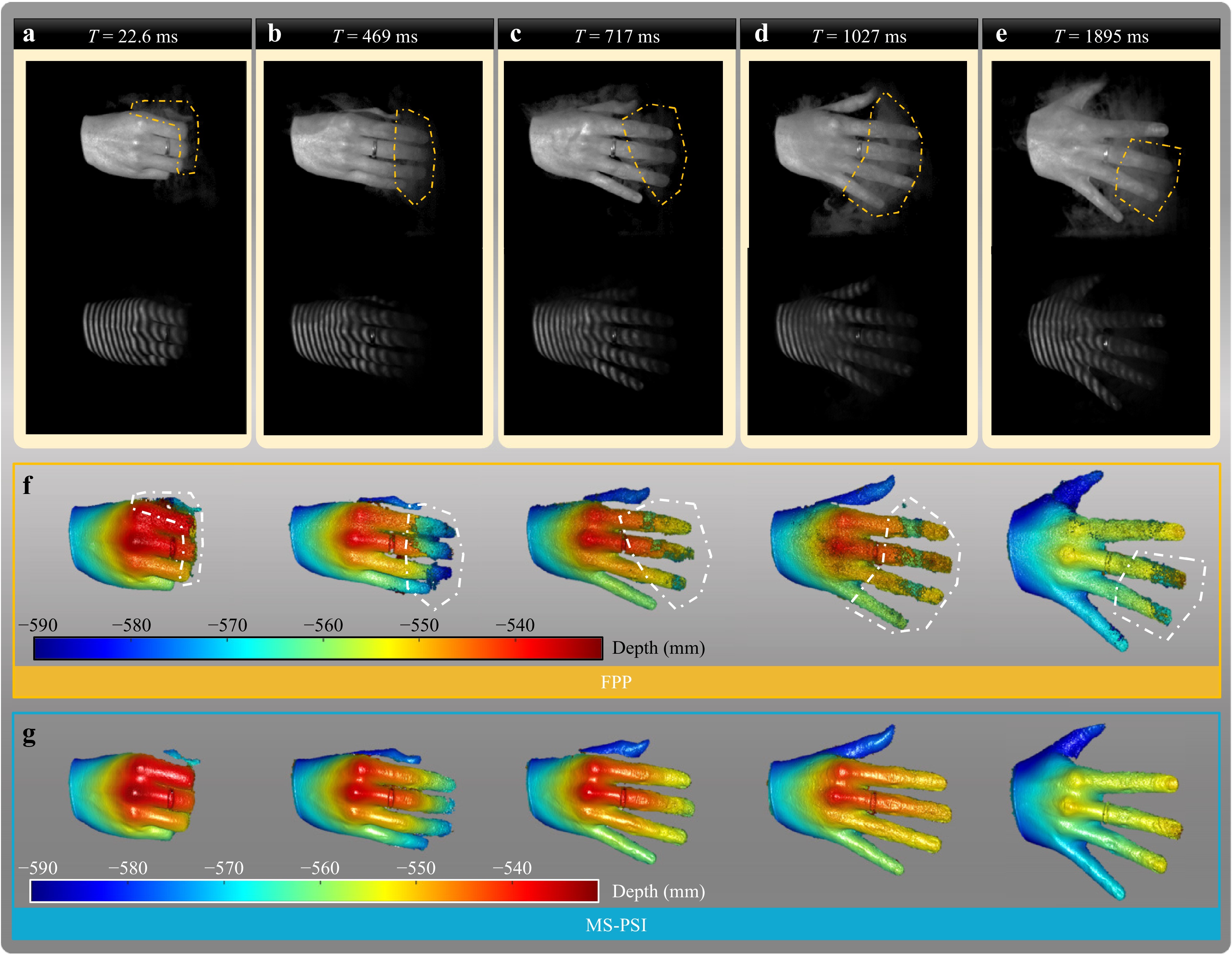
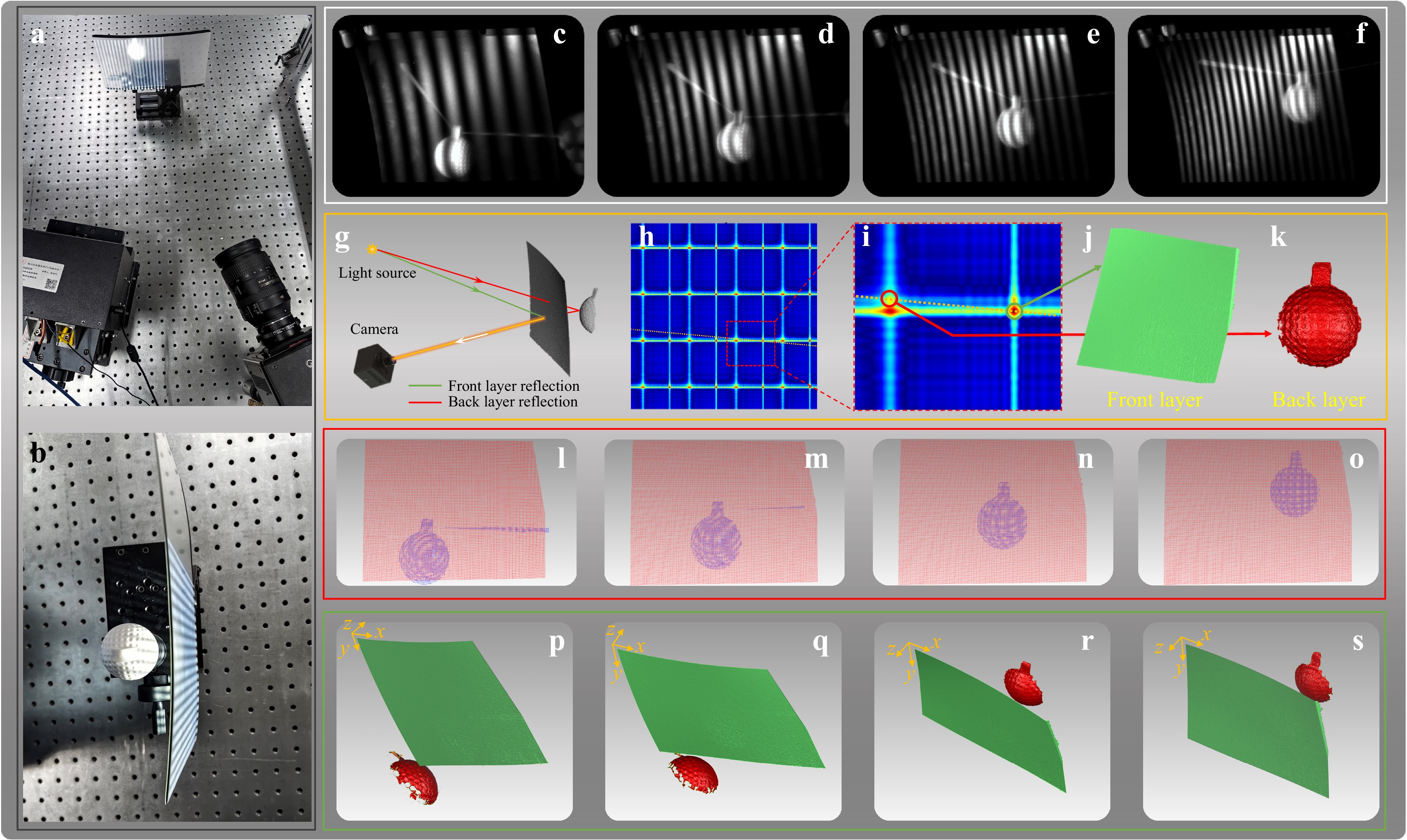
Depth measurement and three-dimensional (3D) imaging under complex reflection and transmission conditions are challenging and even impossible for traditional structured light techniques, owing to the precondition of point-to-point triangulation. Despite recent progress in addressing this problem, there is still no efficient and general solution. Herein, a Fourier dual-slice projection with depth-constrained localization is presented to separate and utilize different illumination and reflection components efficiently, which can significantly decrease the number of projection patterns in each sequence from thousands to fifteen. Subsequently, multi-scale parallel single-pixel imaging (MS-PSI) is proposed based on the established and proven position-invariant theorem, which breaks the local regional assumption and enables dynamic 3D reconstruction. Our methodology successfully unveils unseen-before capabilities such as (1) accurate depth measurement under interreflection and subsurface scattering conditions, (2) dynamic measurement of the time-varying high-dynamic-range scene and through thin volumetric scattering media at a rate of 333 frames per second; (3) two-layer 3D imaging of the semitransparent surface and the object hidden behind it. The experimental results confirm that the proposed method paves the way for dynamic 3D reconstruction under complex optical field reflection and transmission conditions, benefiting imaging and sensing applications in advanced manufacturing, autonomous driving, and biomedical imaging.
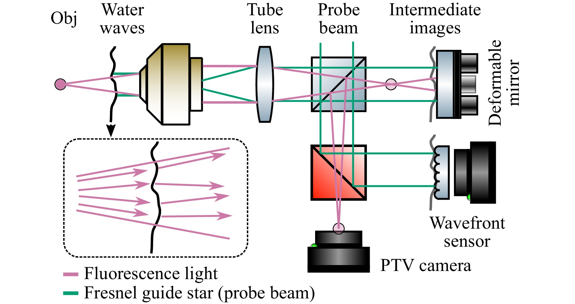
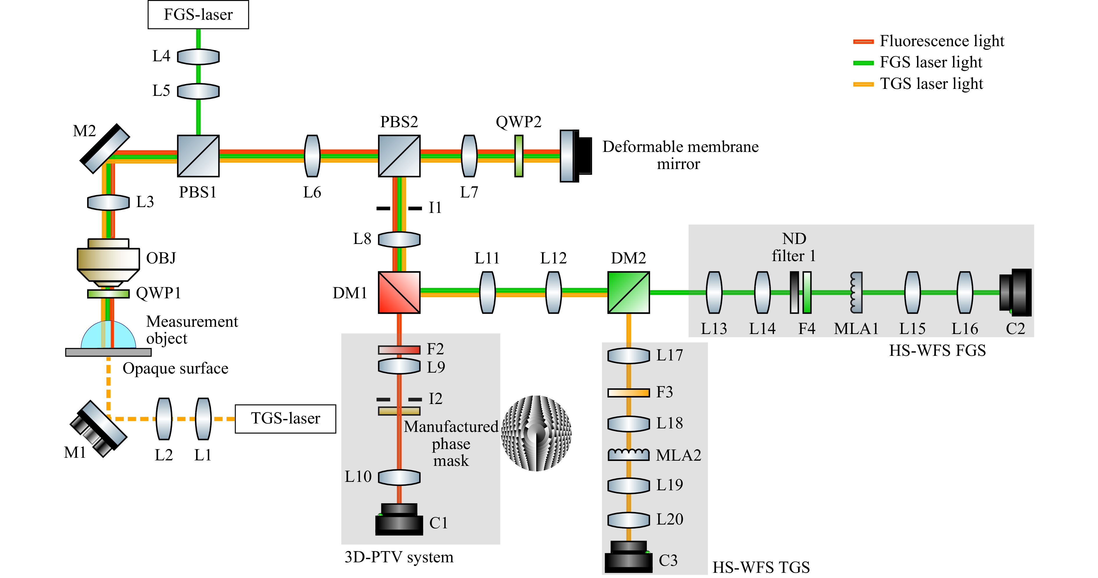
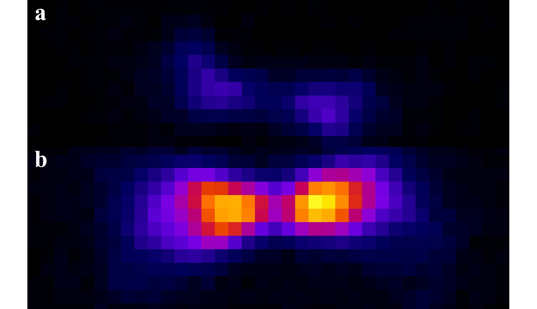
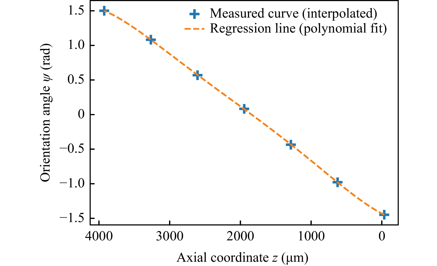
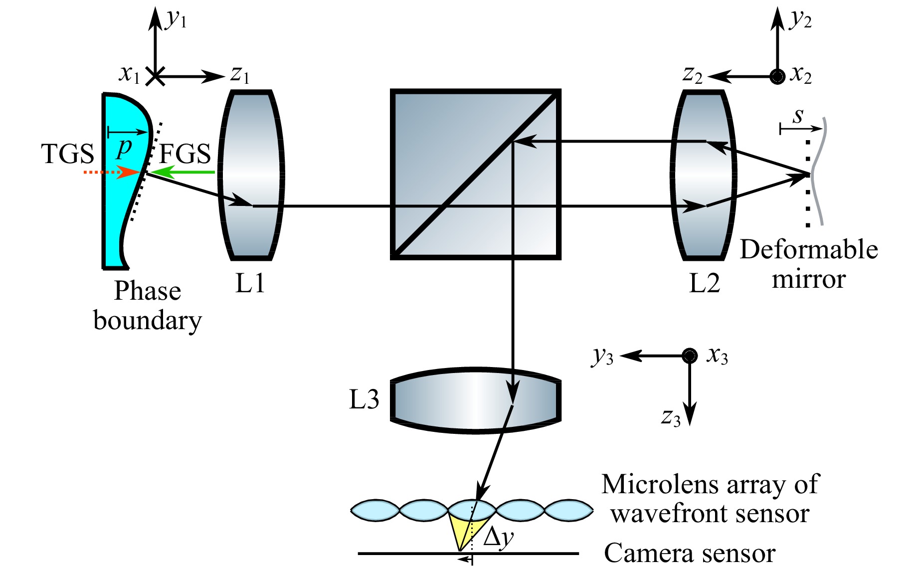
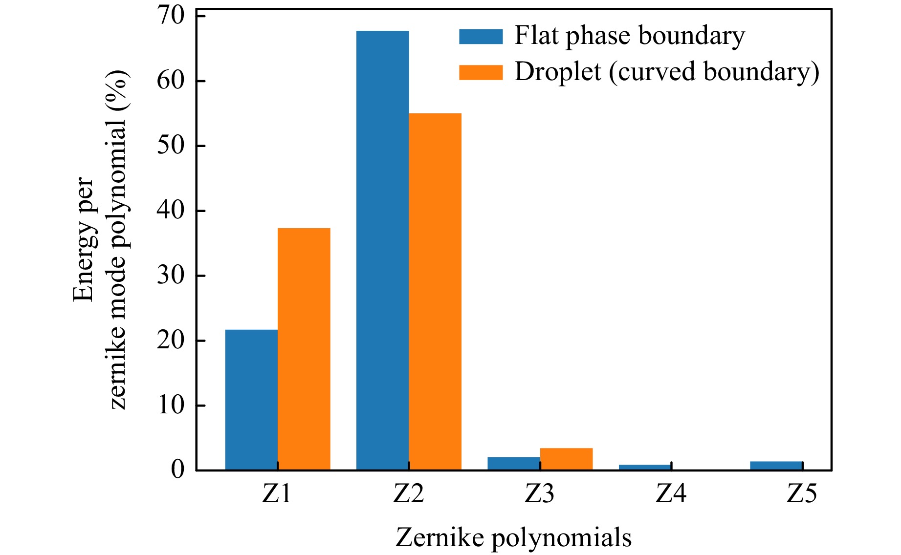
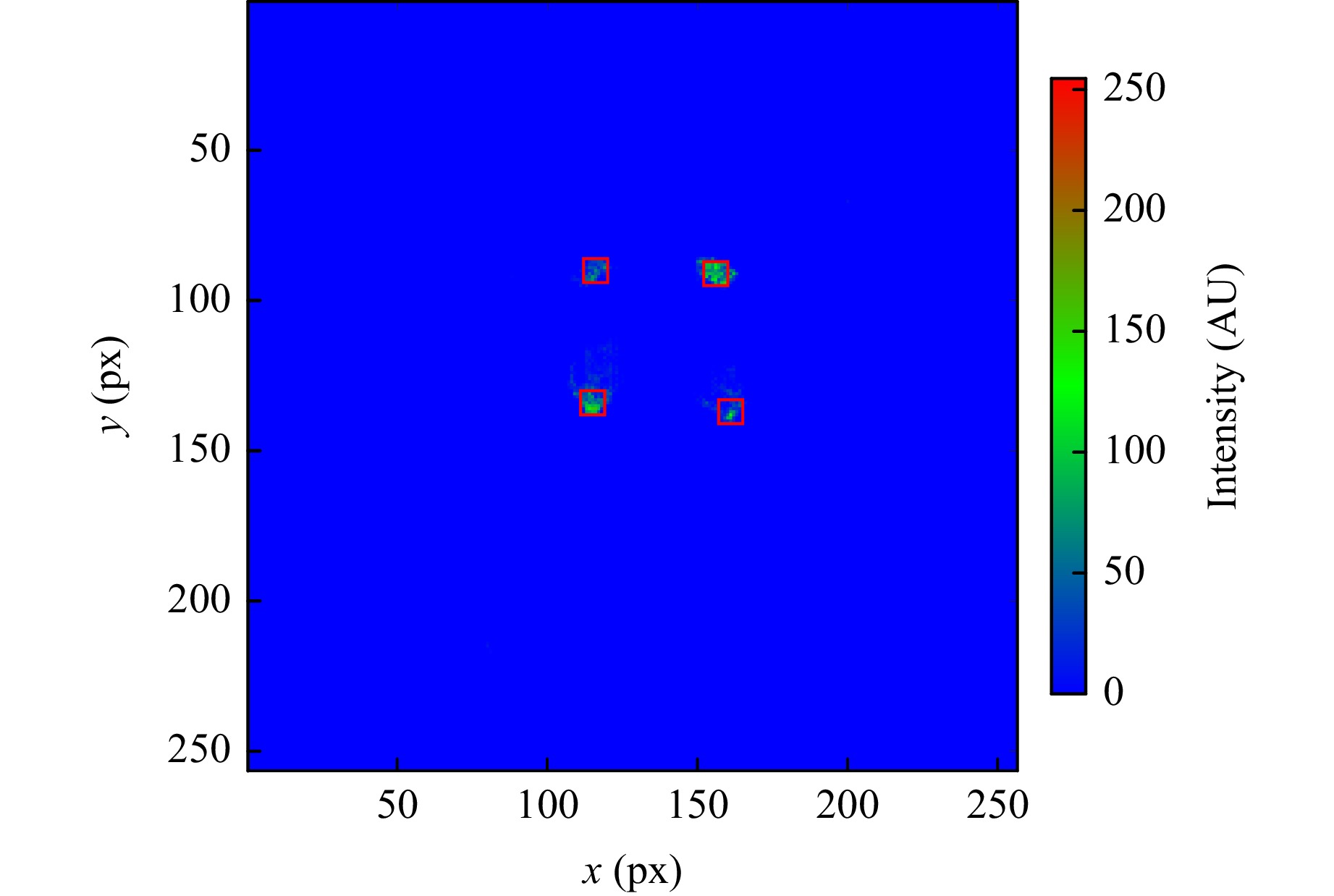
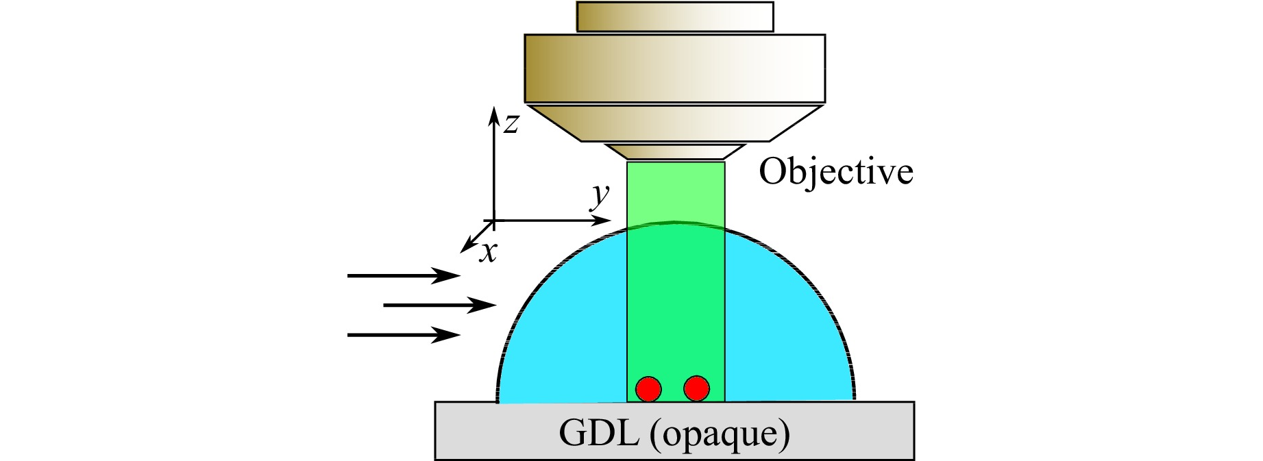
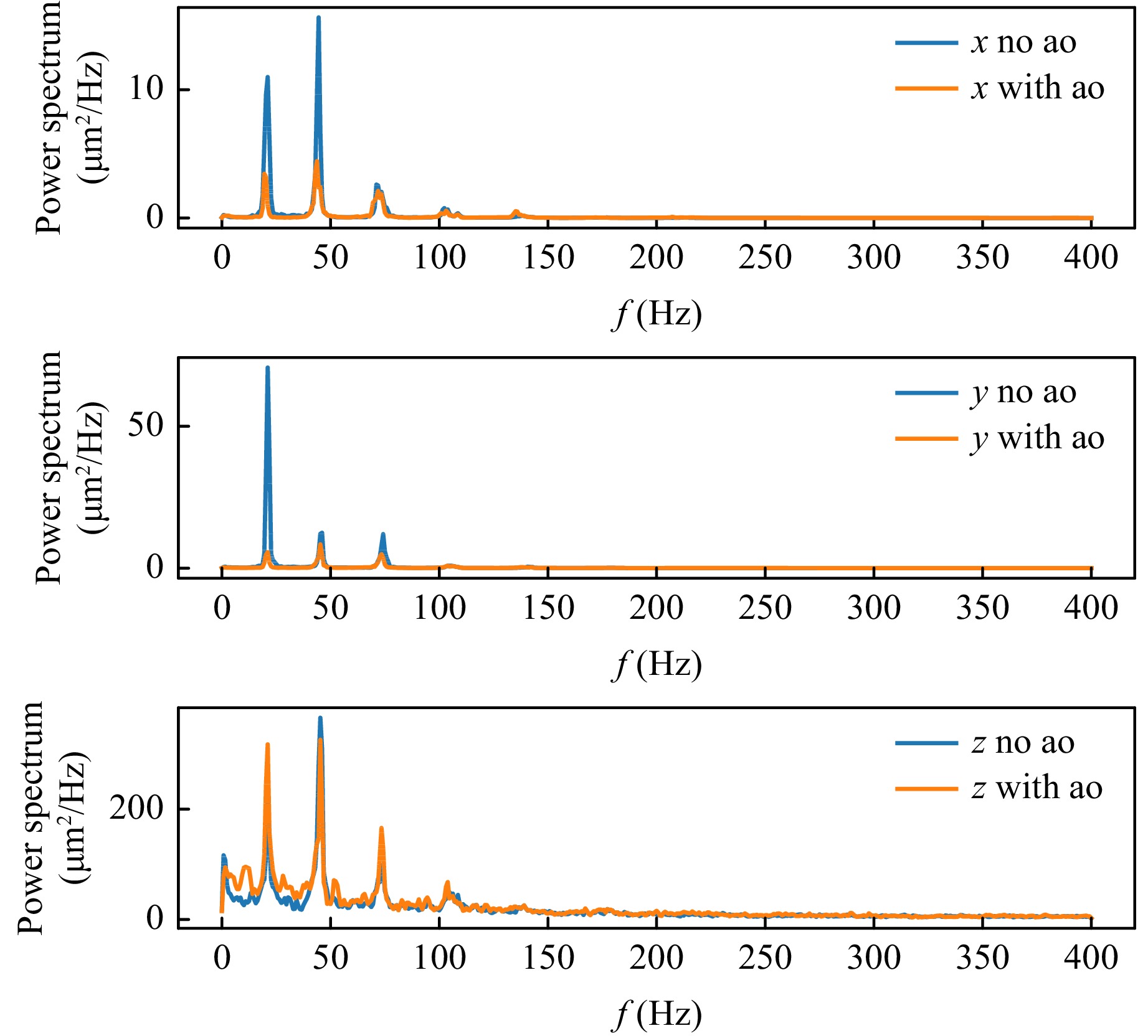
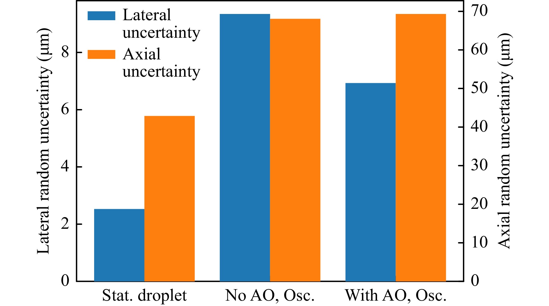
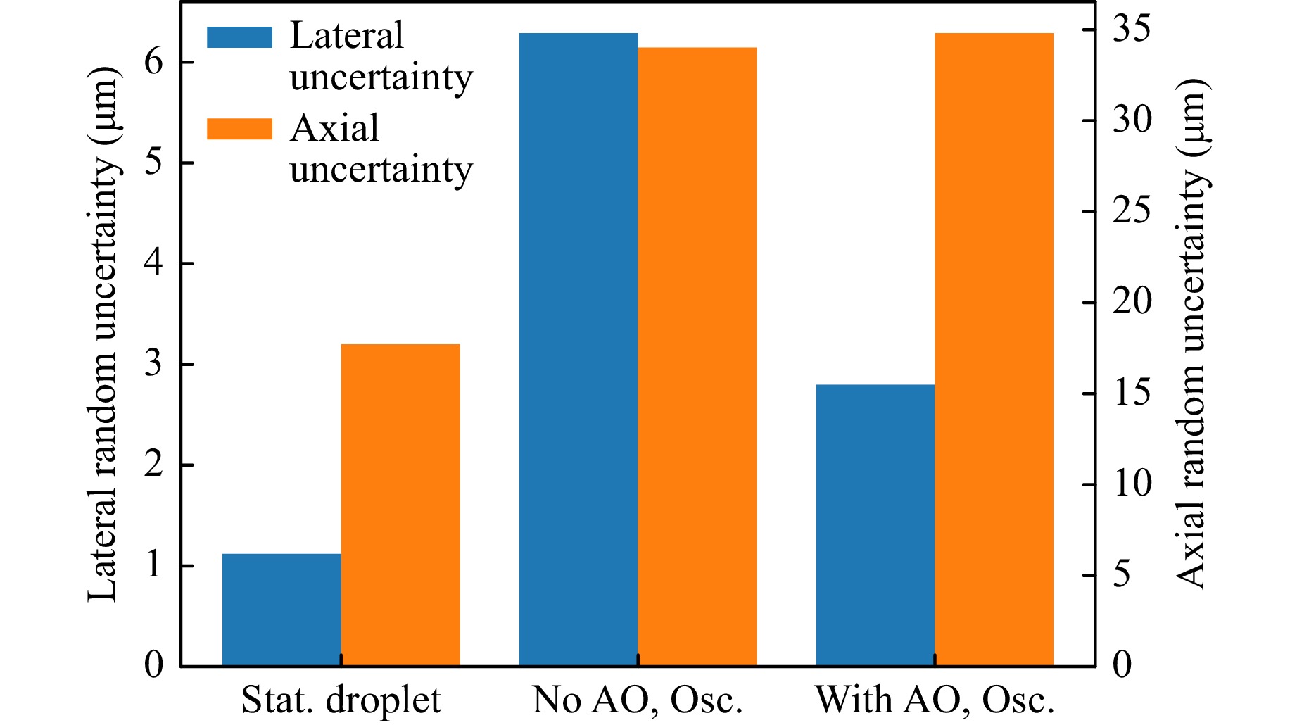
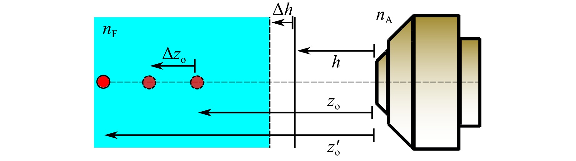
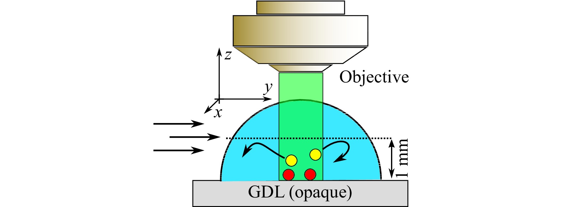
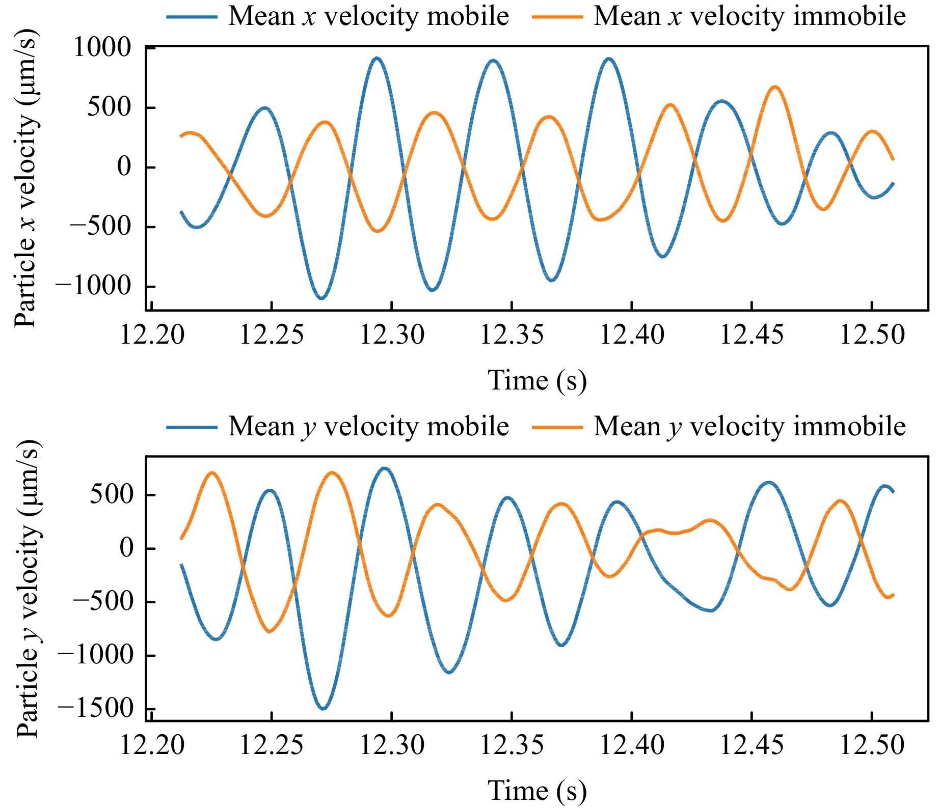
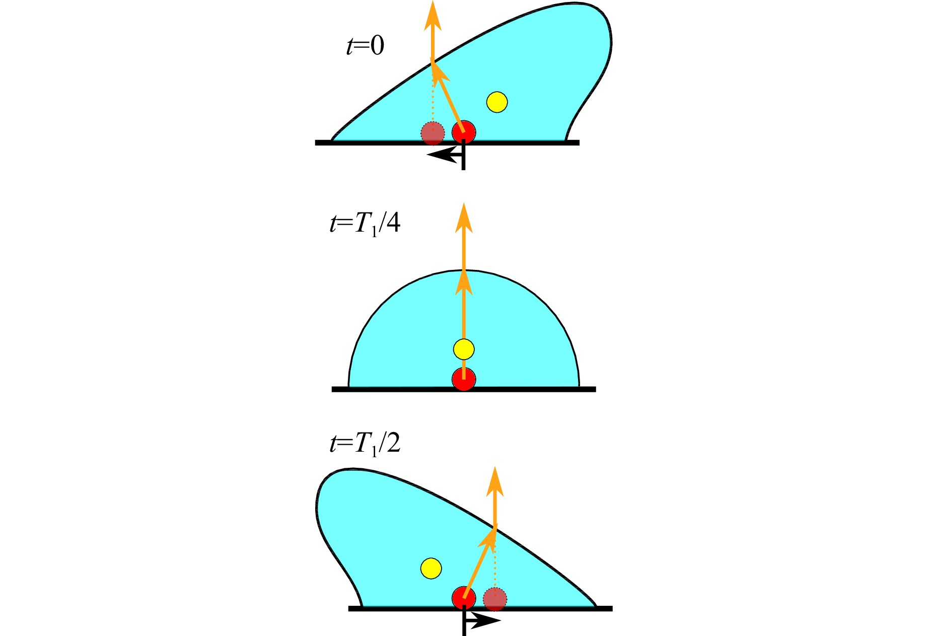
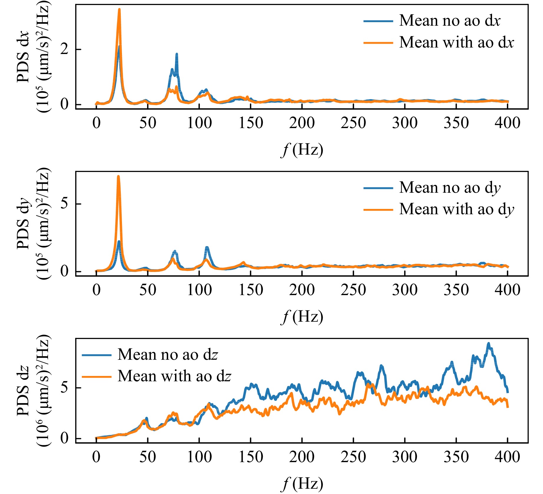
Measurements based on optical microscopy can be severely impaired if the access exhibits variations of the refractive index. In the case of fluctuating liquid-gas boundaries, refraction introduces dynamical aberrations that increase the measurement uncertainty. This is prevalent at multiphase flows (e. g. droplets, film flows) that occur in many technical applications as for example in coating and cleaning processes and the water management in fuel cells. In this paper, we present a novel approach based on adaptive optics for correcting the dynamical aberrations in real time and thus reducing the measurement uncertainty. The shape of the fluctuating water-air interface is sampled with a reflecting light beam (Fresnel Guide Star) and a Hartmann-Shack sensor which makes it possible to correct its influence with a deformable mirror in a closed loop. Three-dimensional flow measurements are achieved by using a double-helix point spread function. We measure the flow inside a sessile, oscillating 50-μl droplet on an opaque gas diffusion layer for fuel cells and show that the temporally varying refraction at the droplet surface causes a systematic underestimation of the flow field magnitude corresponding to the first droplet eigenmode which plays a major role in their detachment mechanism. We demonstrate that the adaptive optics correction is able to reduce this systematic error. Hence, the adaptive optics system can pave the way to a deeper understanding of water droplet formation and detachment which can help to improve the efficiency of fuels cells.


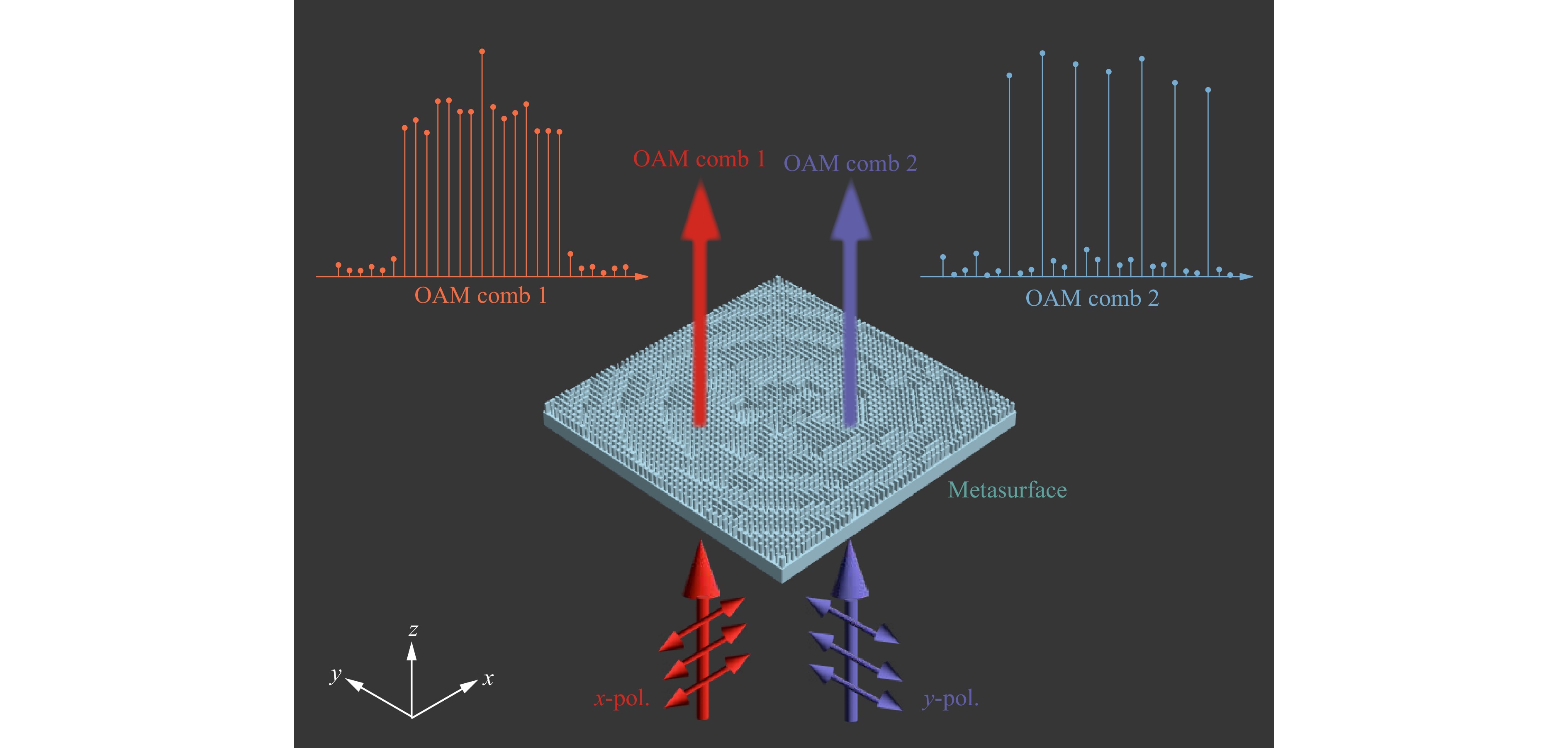
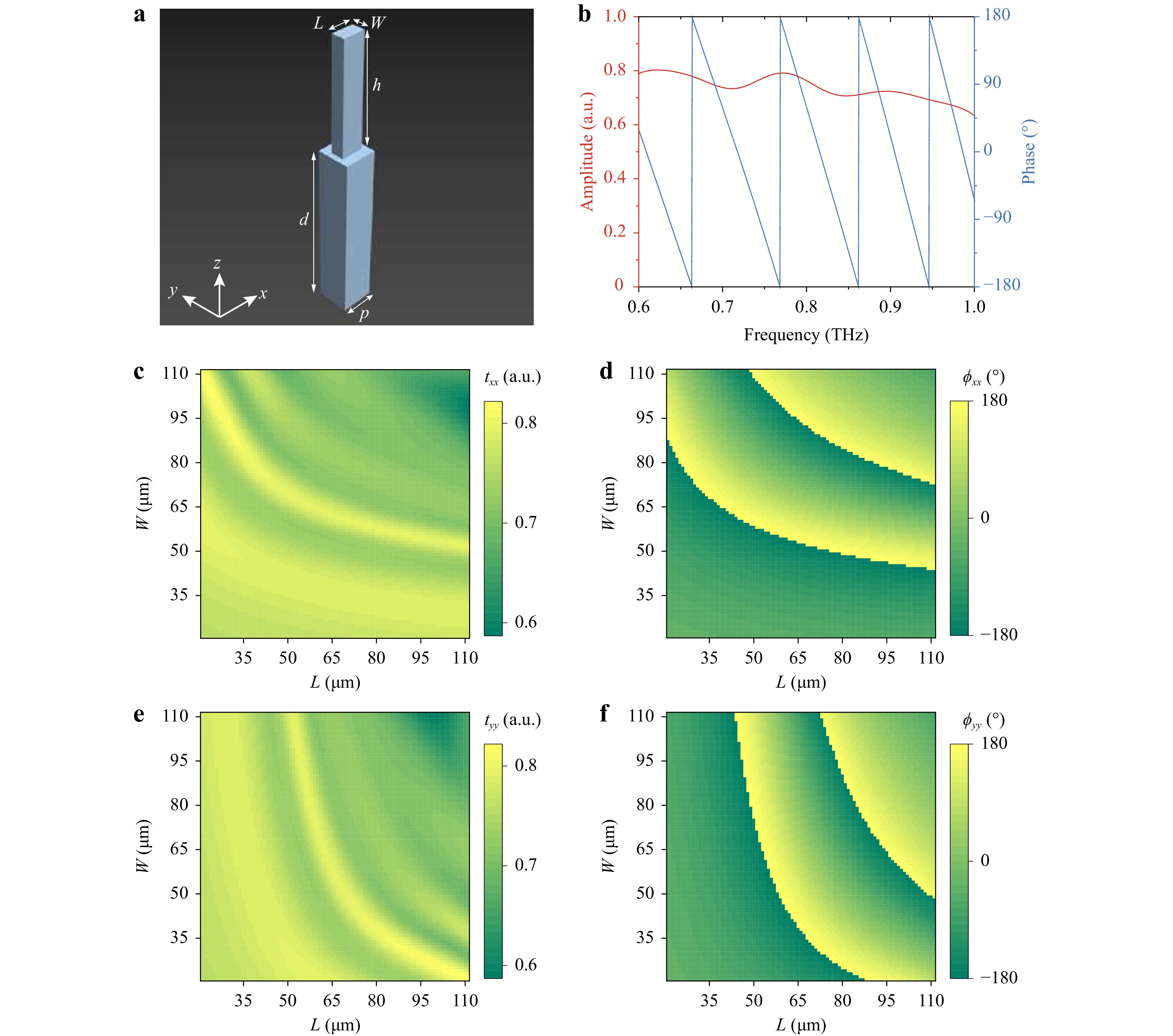
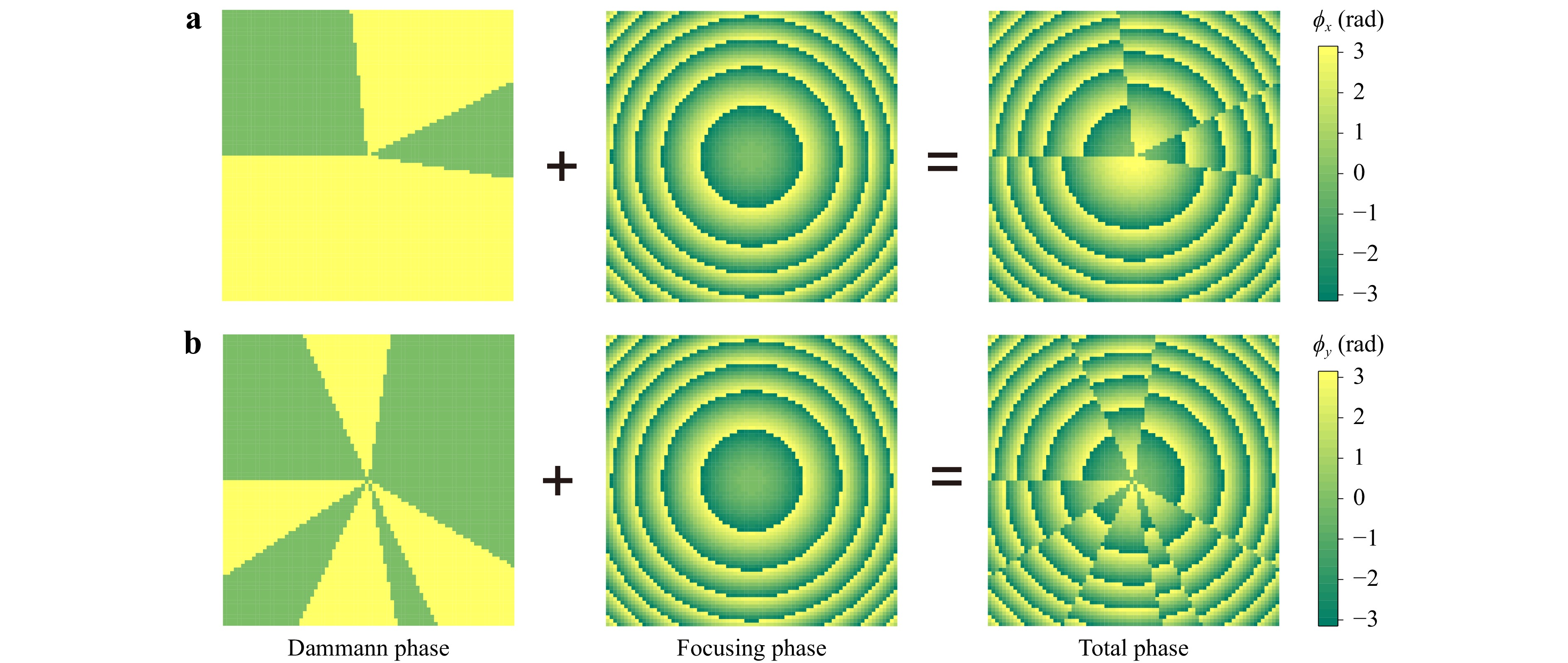
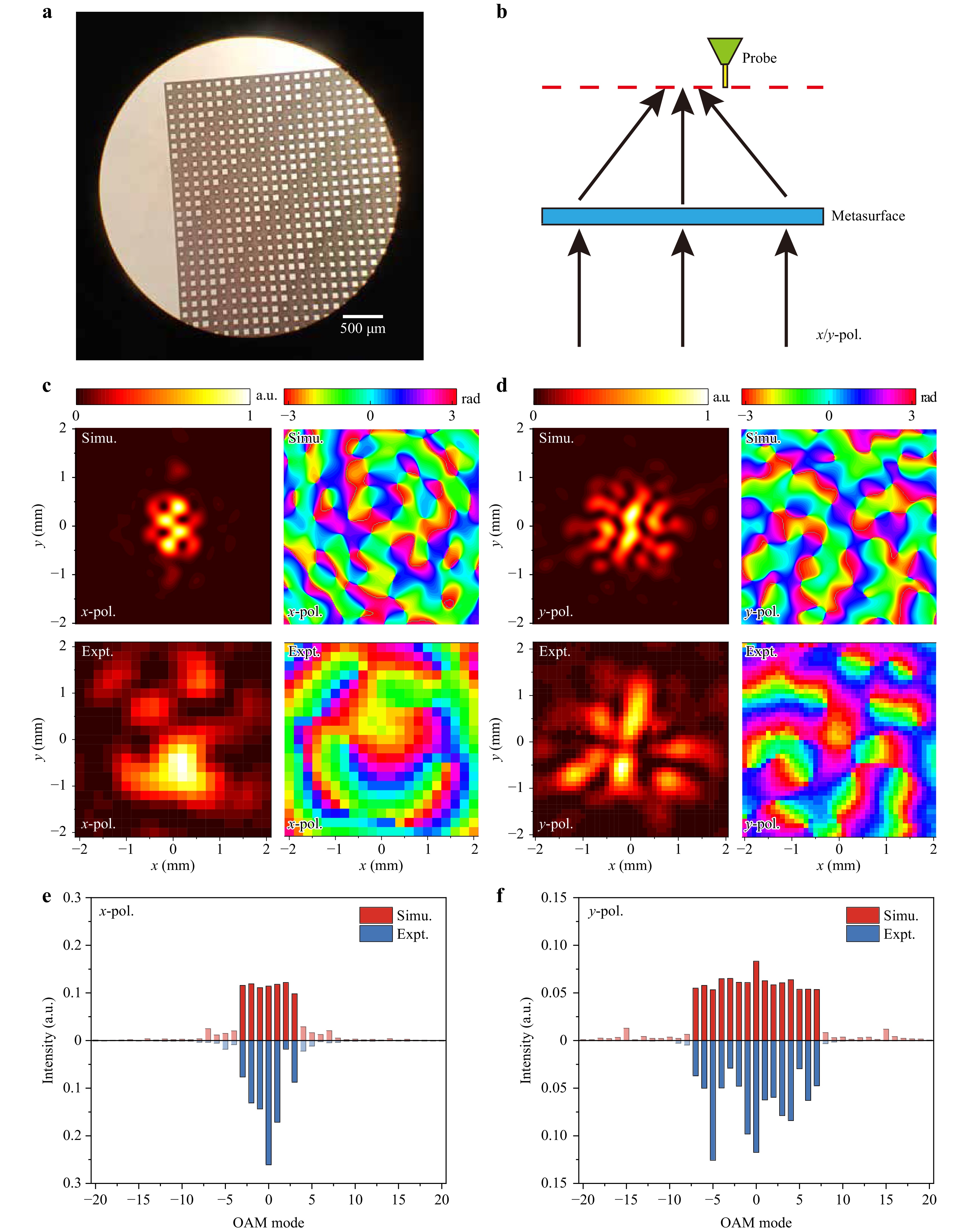
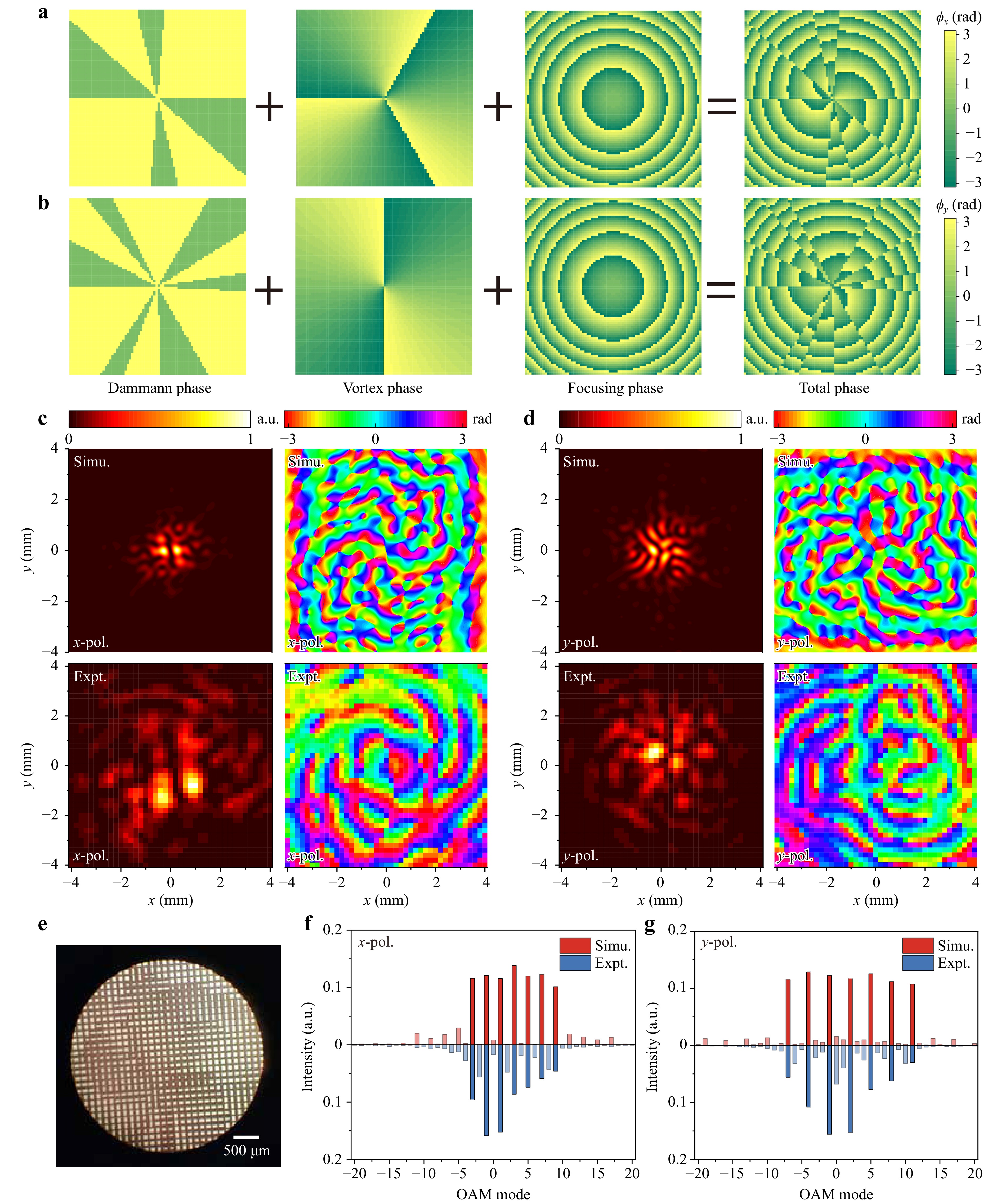
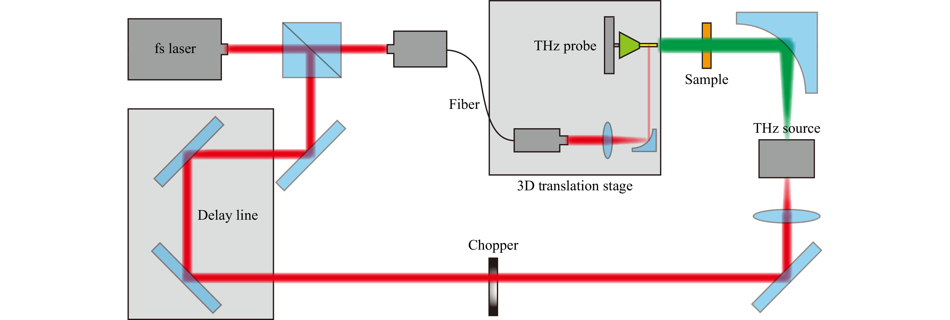
Electromagnetic waves carrying orbital angular momentum (OAM), namely OAM beams, are important in various fields including optics, communications, and quantum information. However, most current schemes can only generate single or several simple OAM modes. Multi-mode OAM beams are rarely seen. This paper proposes a scheme to design metasurfaces that can generate multiple polarization-multiplexed OAM modes with equal intervals and intensities (i.e., OAM combs) working in the terahertz (THz) range. As a proof of concept, we first design a metasurface to generate a pair of polarization-multiplexed OAM combs with arbitrary mode numbers. Furthermore, another metasurface is proposed to realize a pair of polarization-multiplexed OAM combs with arbitrary locations and intervals in the OAM spectrum. Experimental results agree well with full-wave simulations, verifying a great performance of OAM combs generation. Our method may provide a new solution to designing high-capacity THz devices used in multi-mode communication systems.
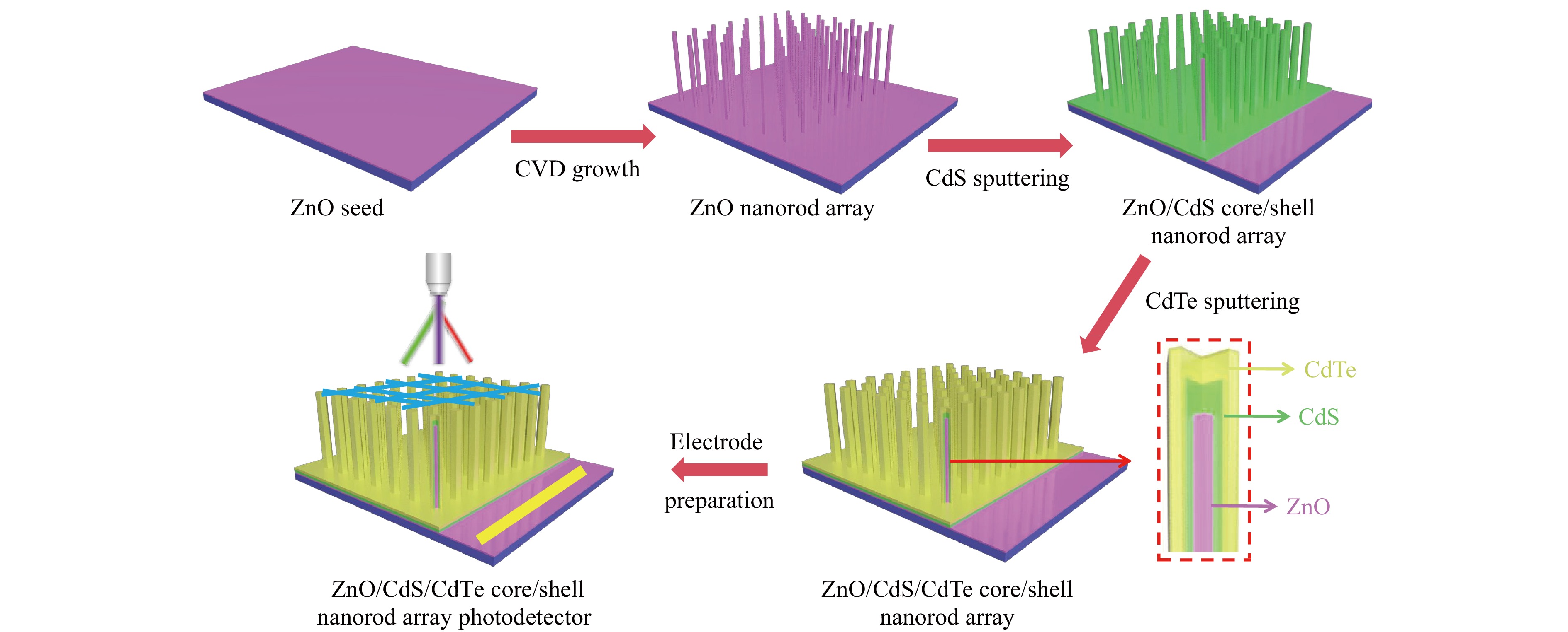
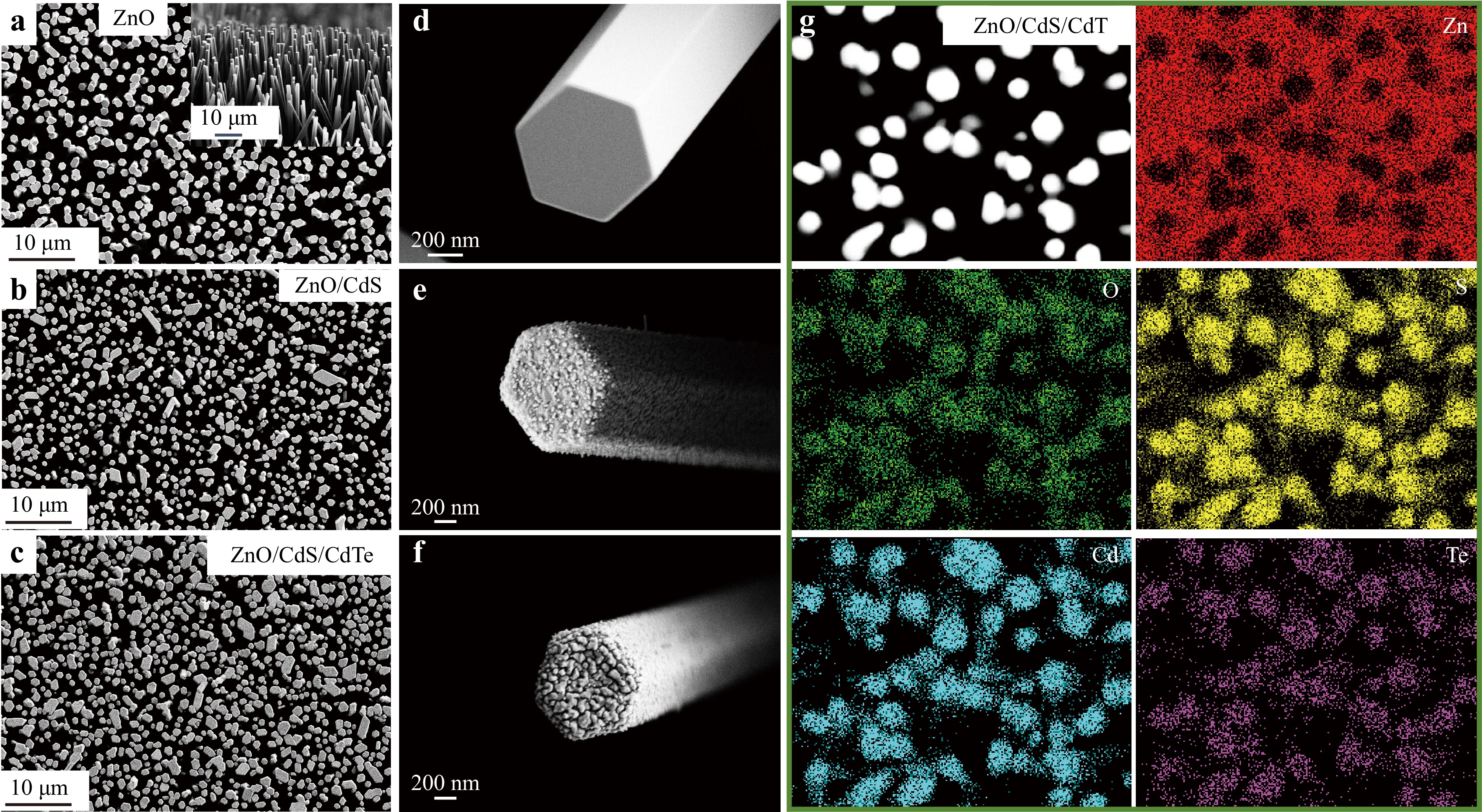
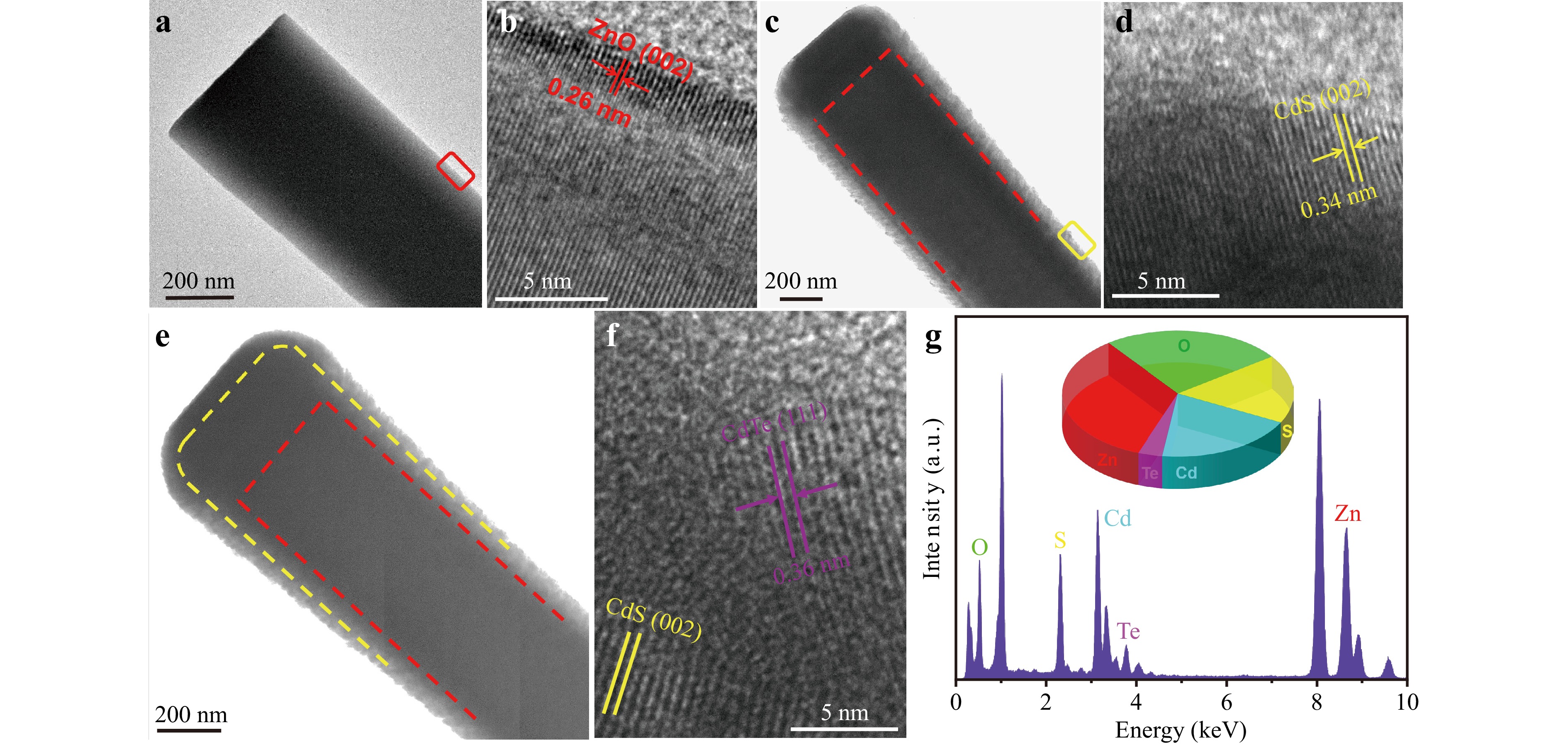
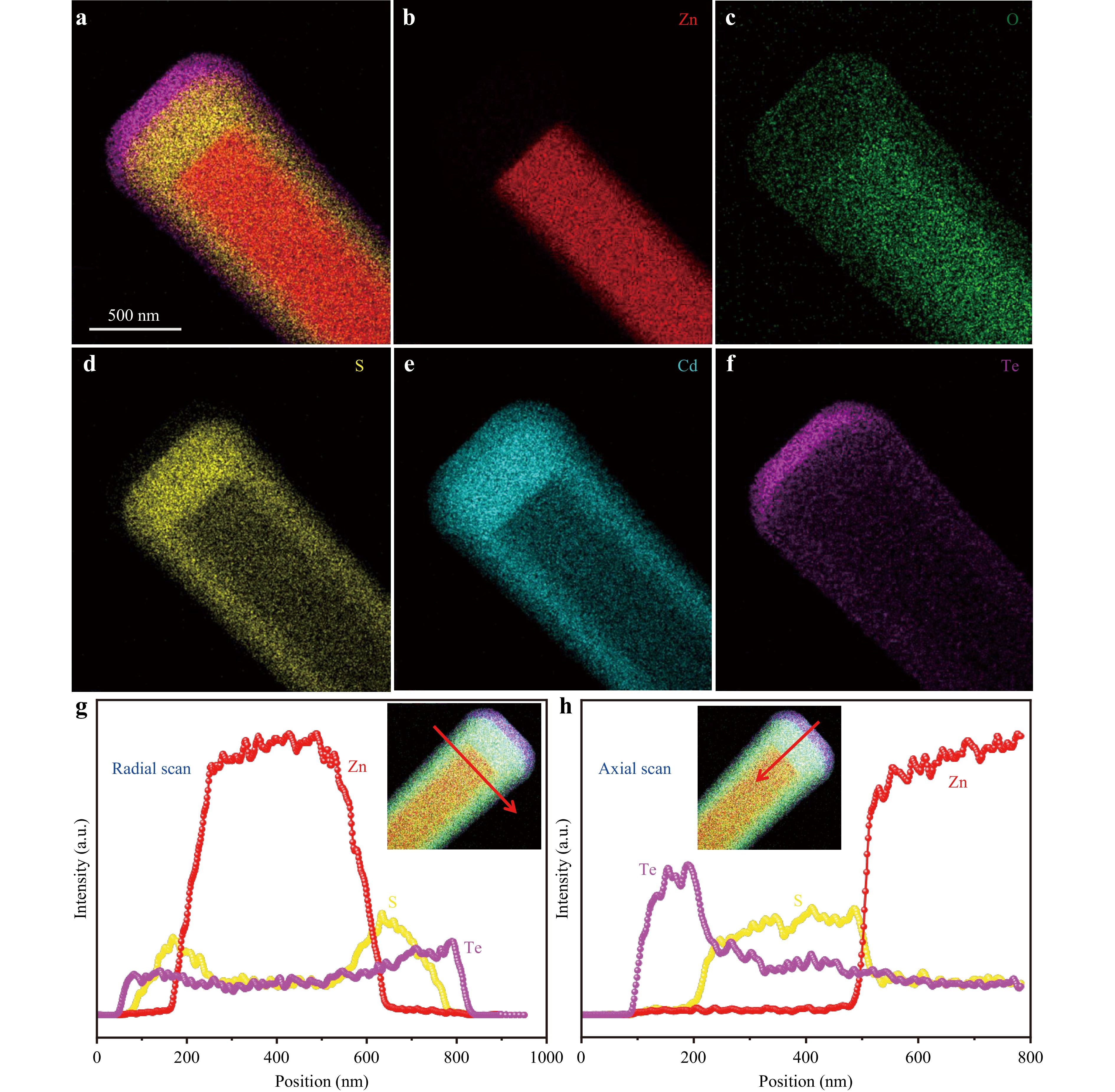
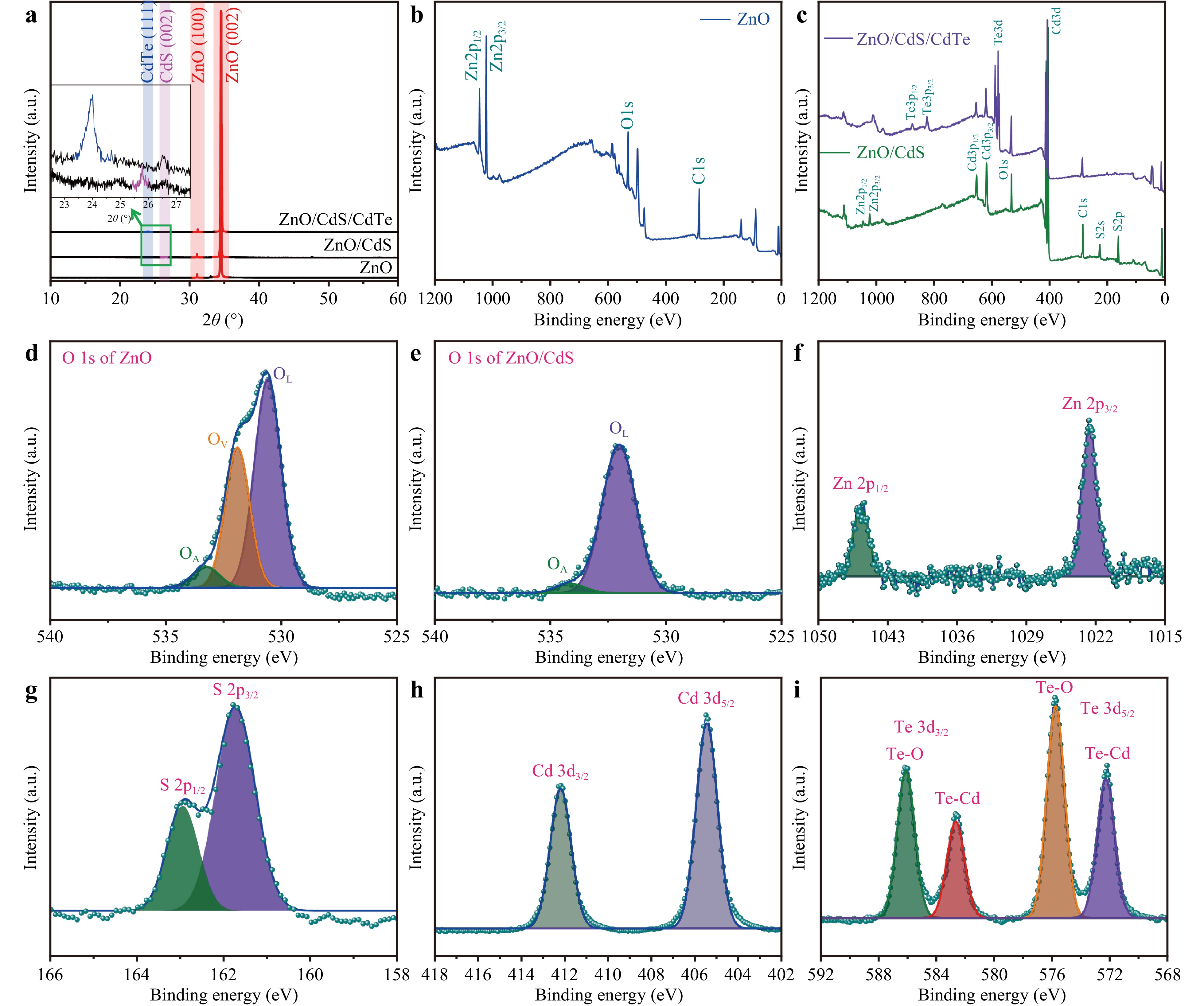
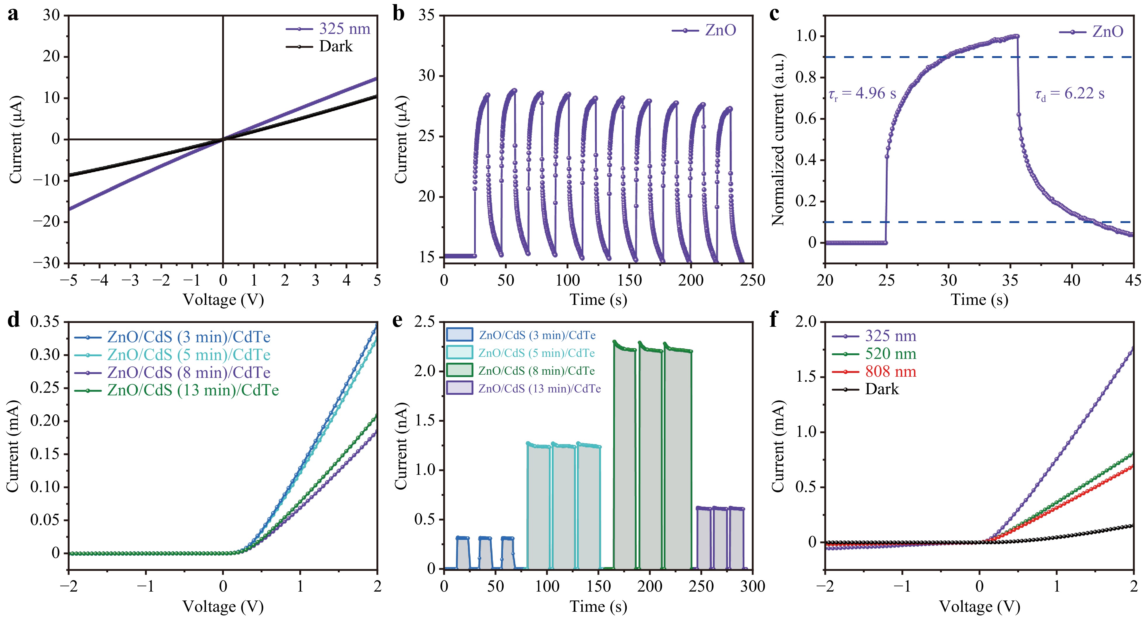
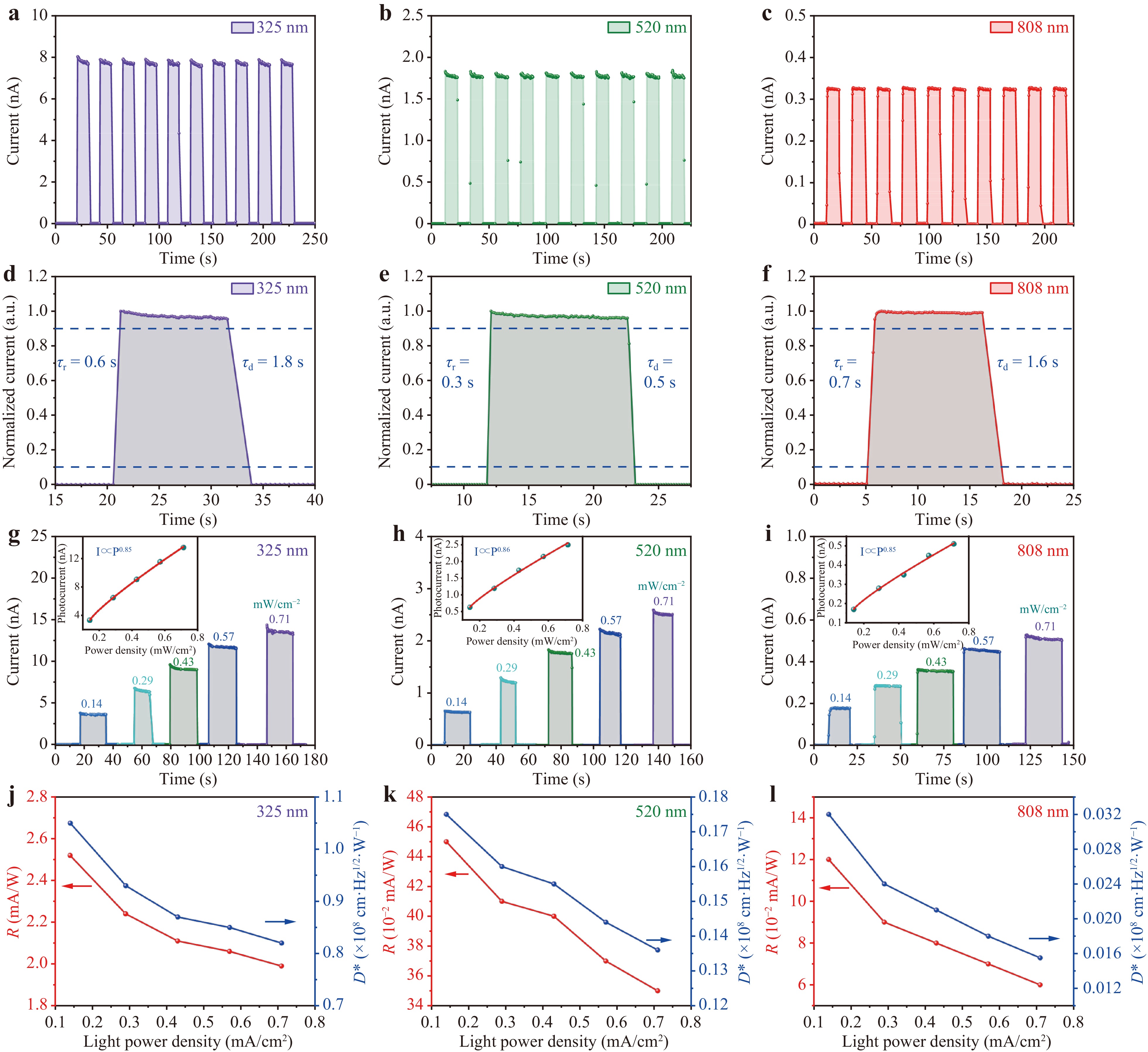
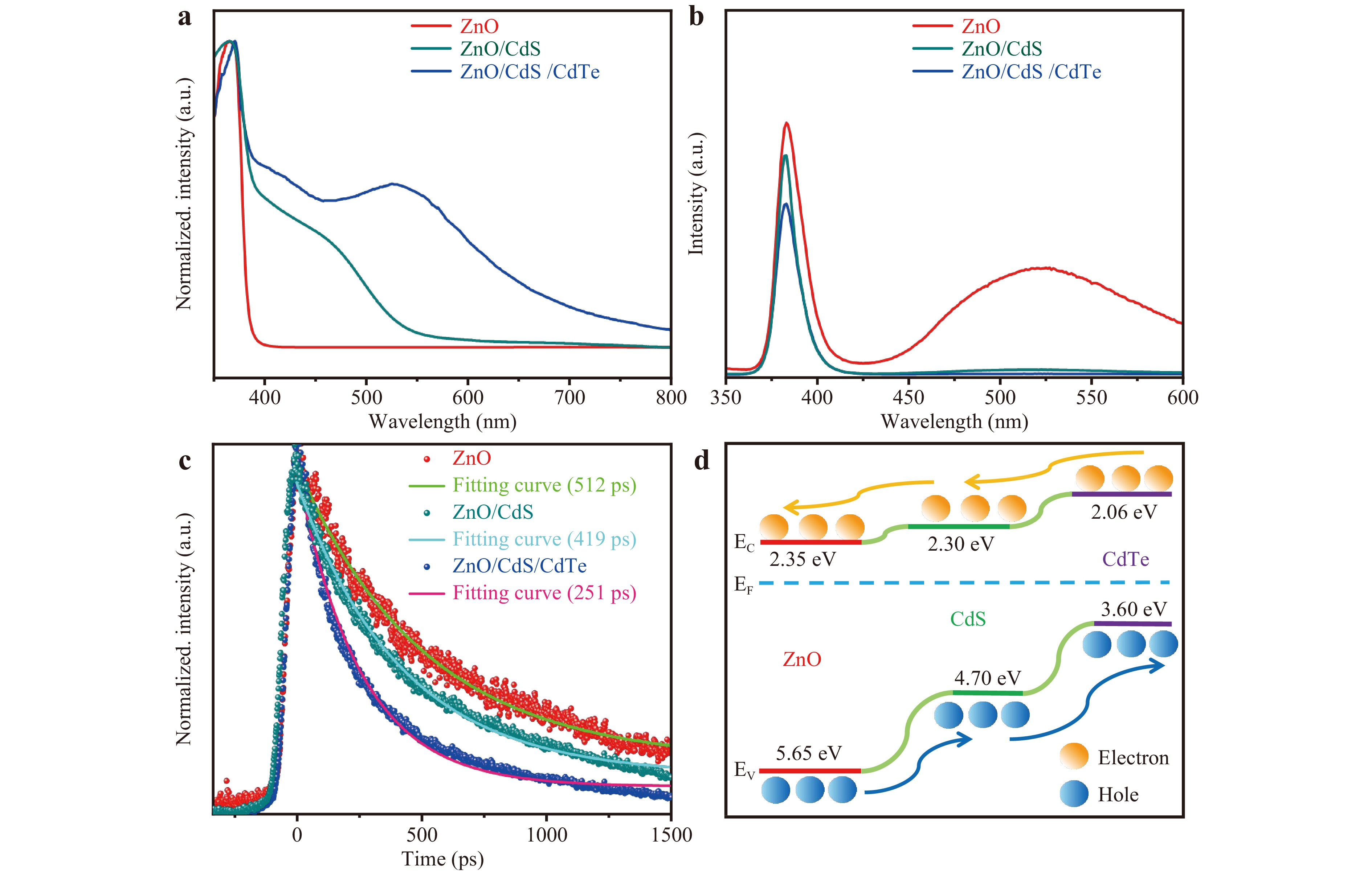
Constructing a one-dimensional (1D) core/shell heterostructure is a rational and efficient way to integrate multiple functional materials into a single device, in which a distinct and reliable interface and suitable energy-band alignment play important roles in optoelectronic applications. Here, using a typical magnetron sputtering system, we constructed a 1D ZnO/CdS/CdTe core/shell nanorod arrays radial heterojunction with a well-designed cascade type-II energy band alignment and improved the broadband photodetector (PD) performance. The well-formed shell layers compensated for the defect states on the ZnO surface and extended the photoresponse range from ultraviolet to visible and near-infrared. Moreover, reliable and distinct heterointerfaces with a cascade type-II energy band alignment can guarantee more stable carrier migration and reduce energy loss, promoting effective photogenerated charge carrier separation and resulting in an enhanced photoresponse. The optimised 1D ZnO/CdS/CdTe core/shell heterojunction PD exhibited a fast photoresponse at 0 V bias with high responsivity and detectivity. These results provide an important reference for the rational design and controllable synthesis of multifunctional optoelectronic nanodevices.
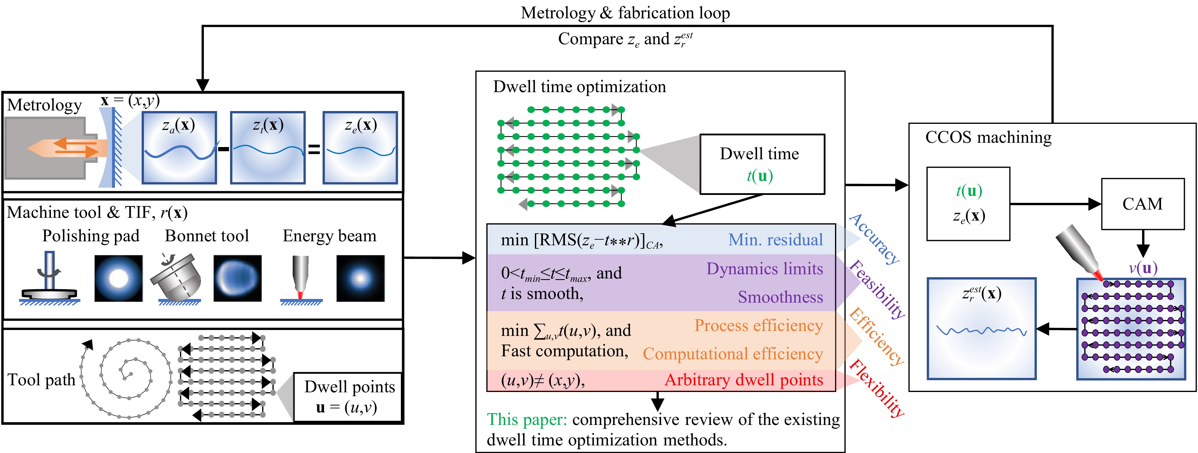
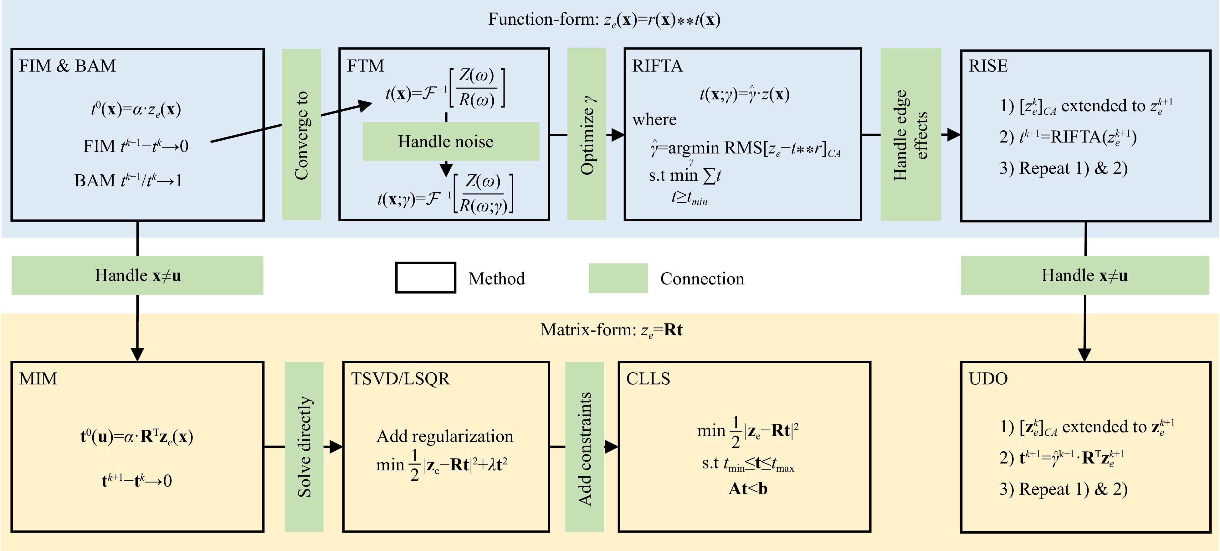
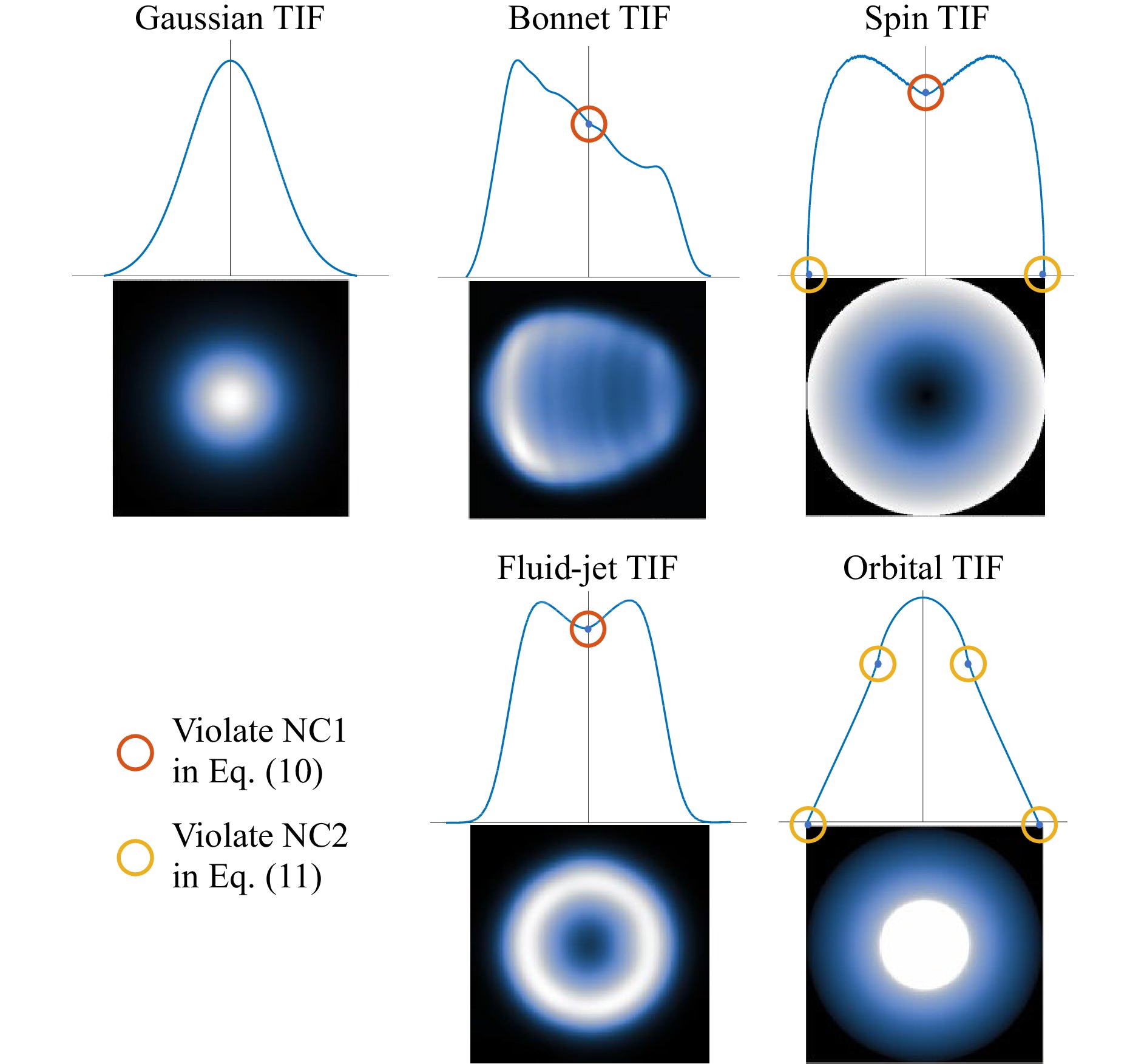
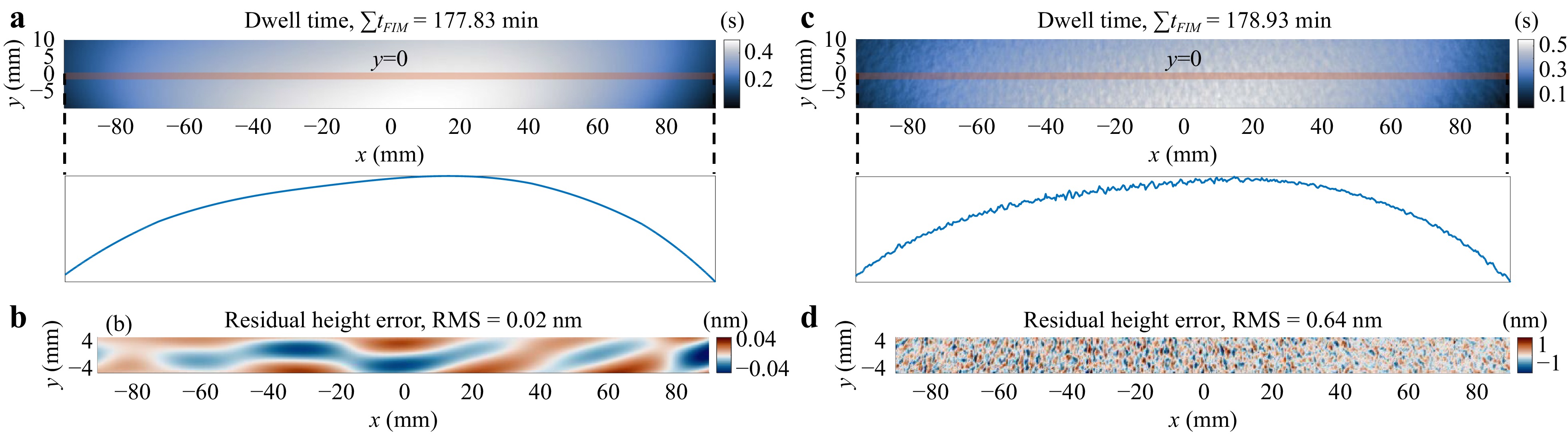
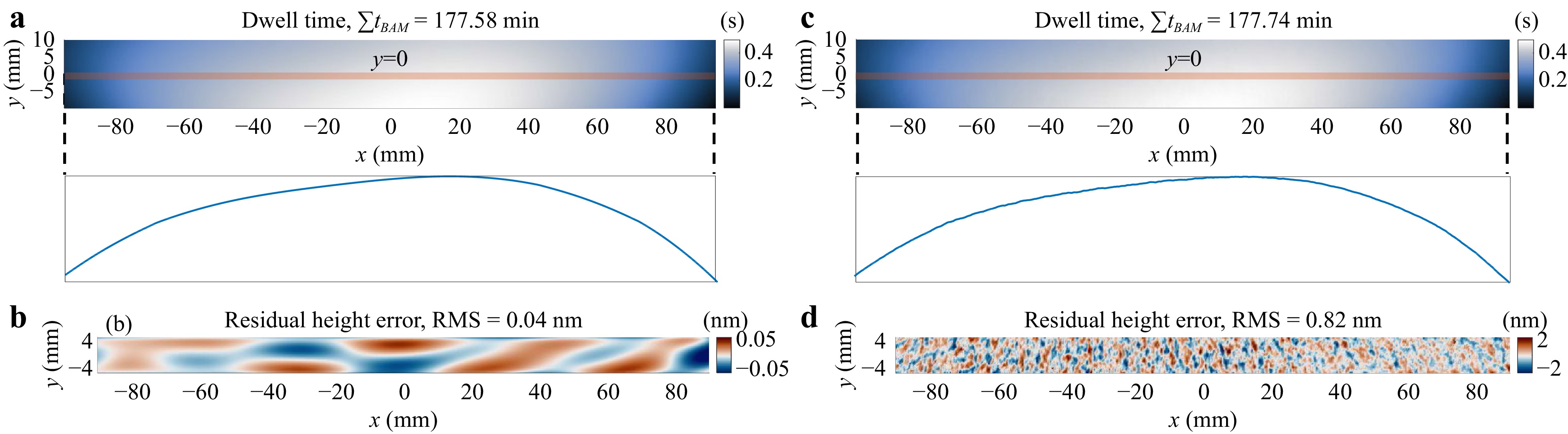
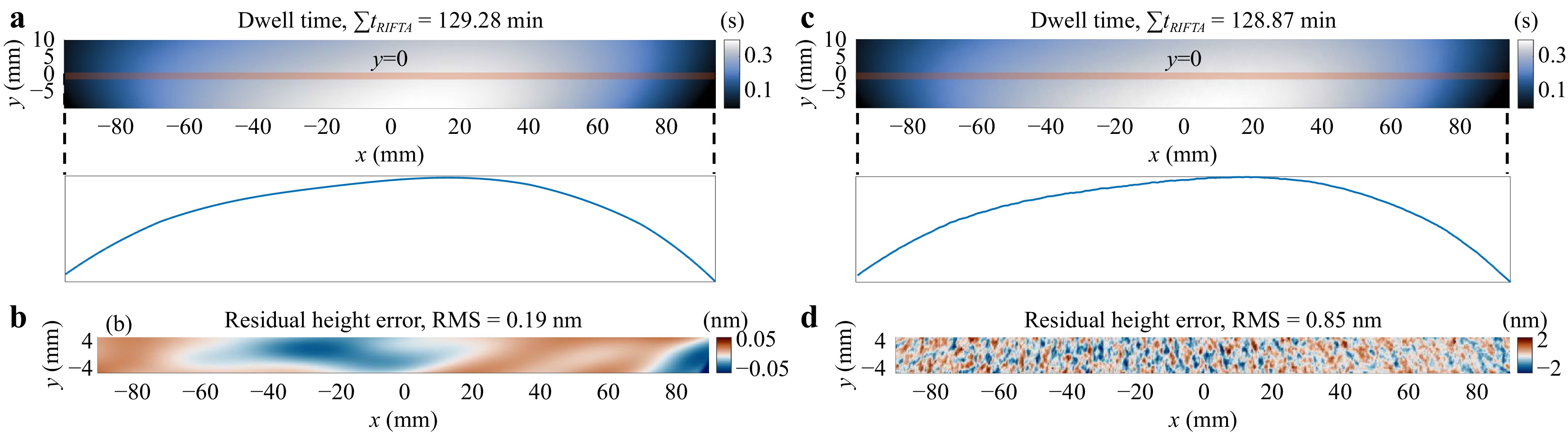
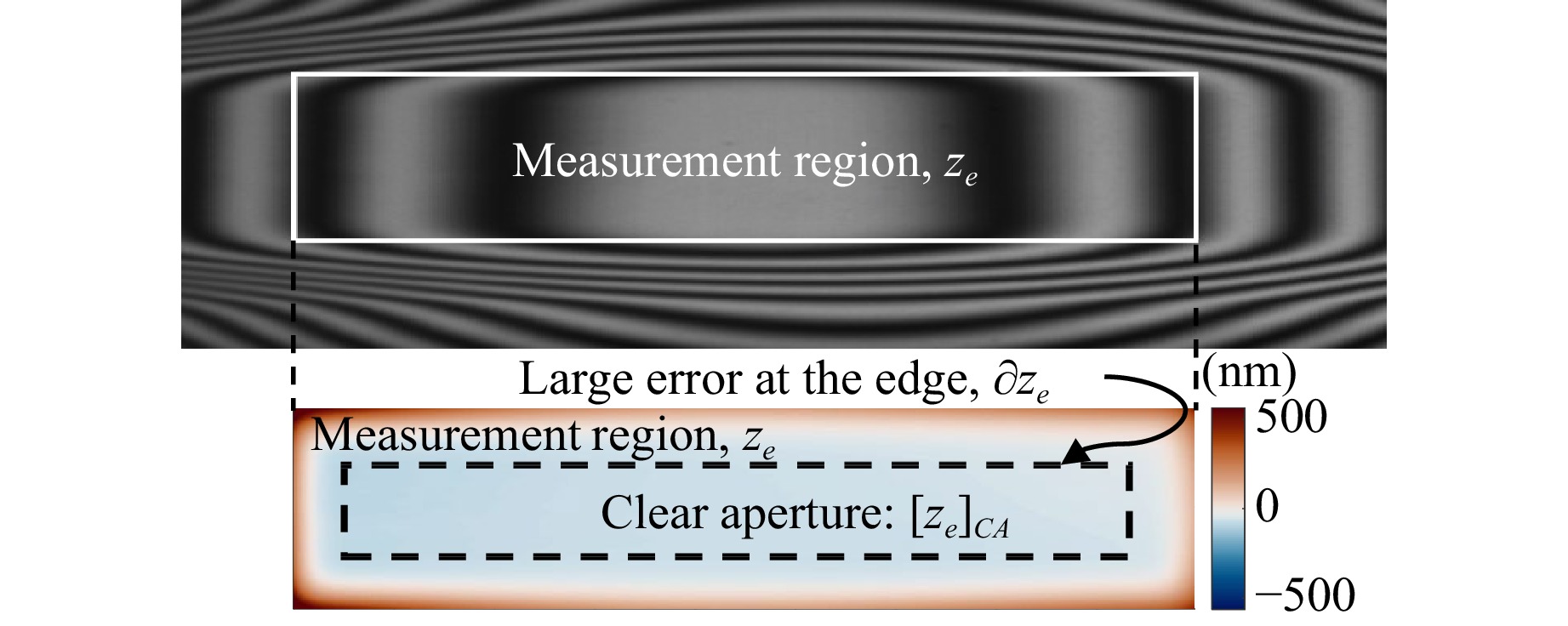
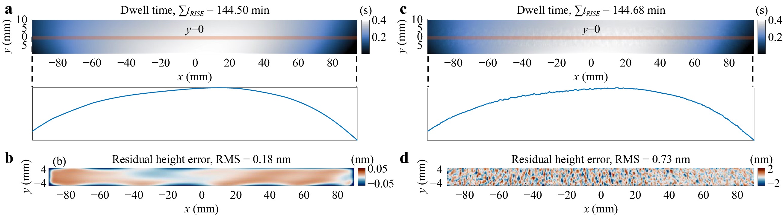
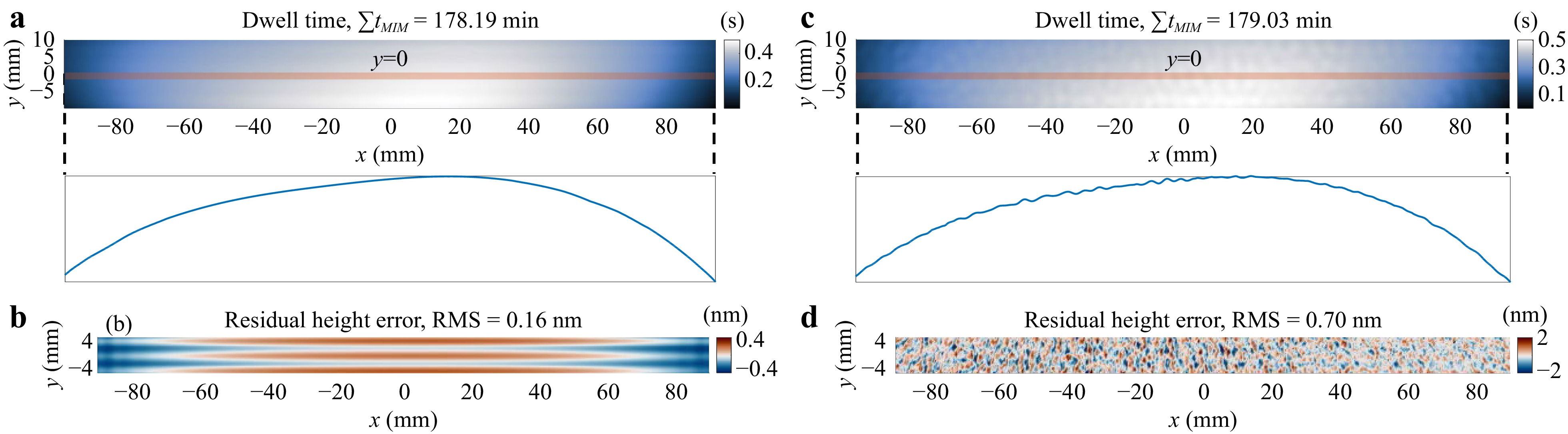
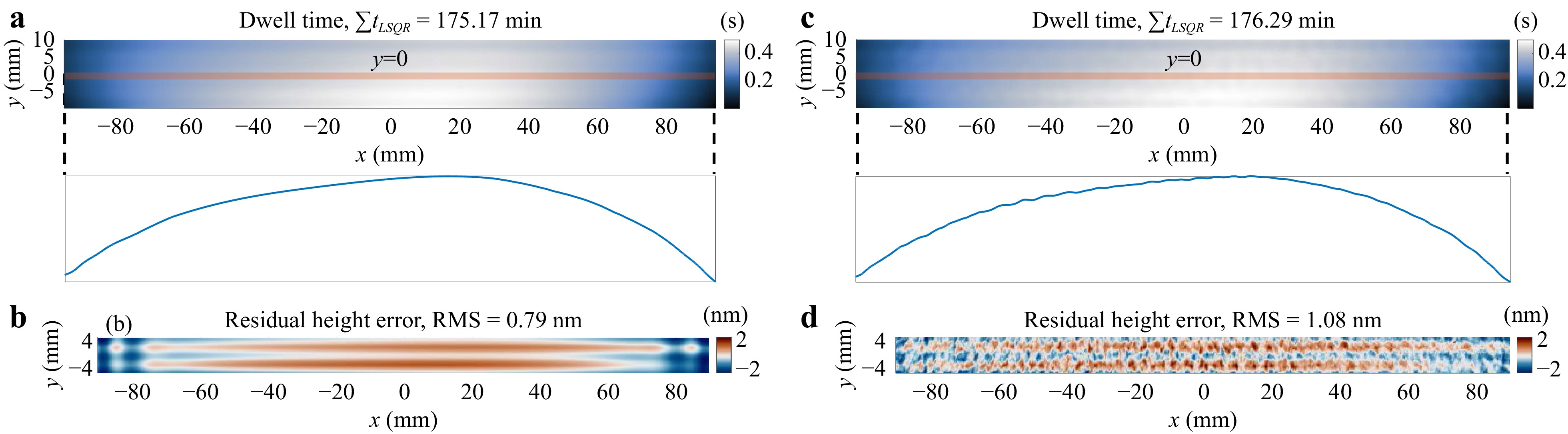
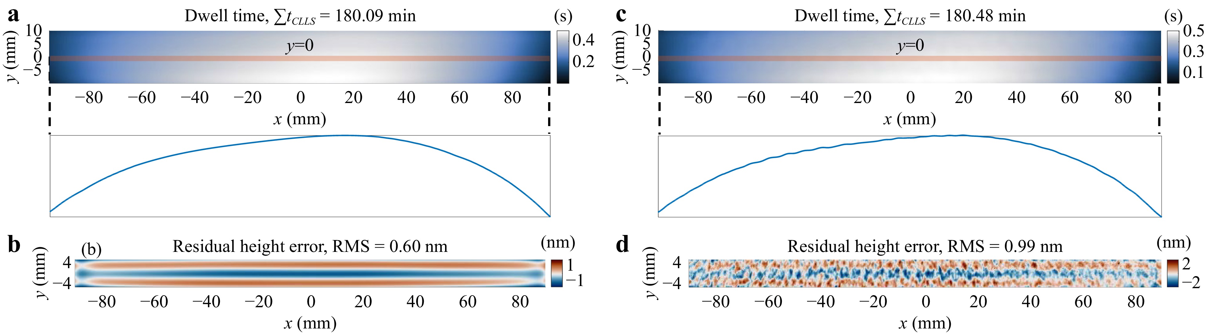
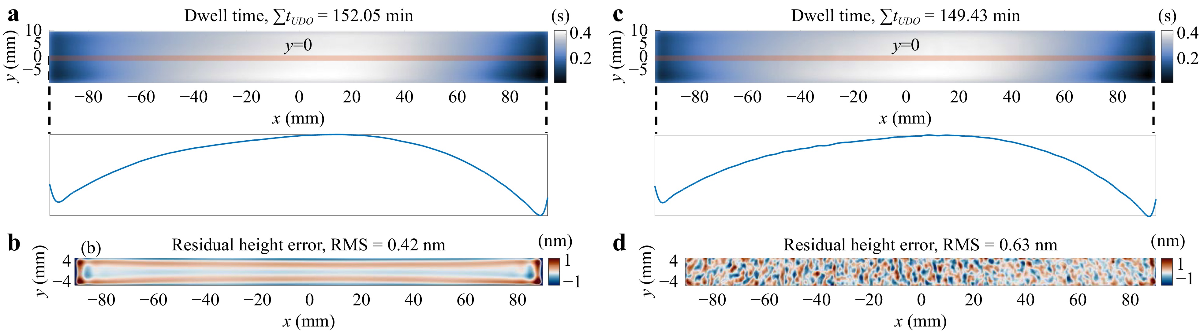
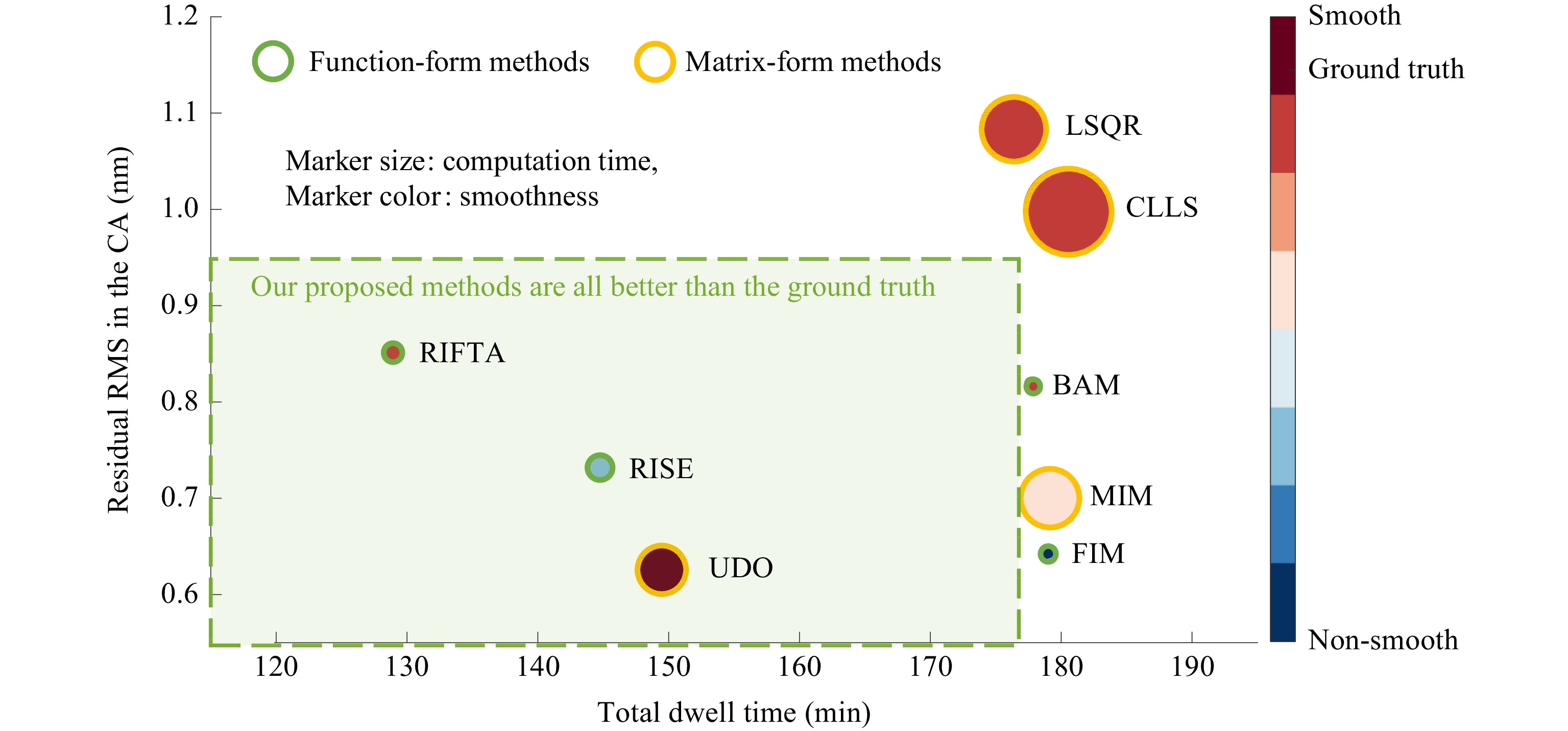
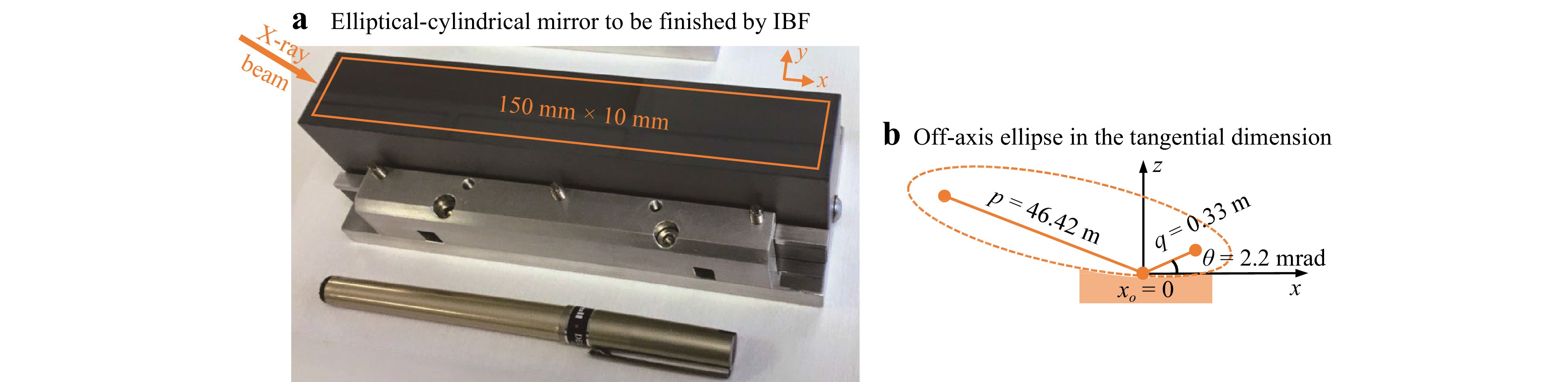
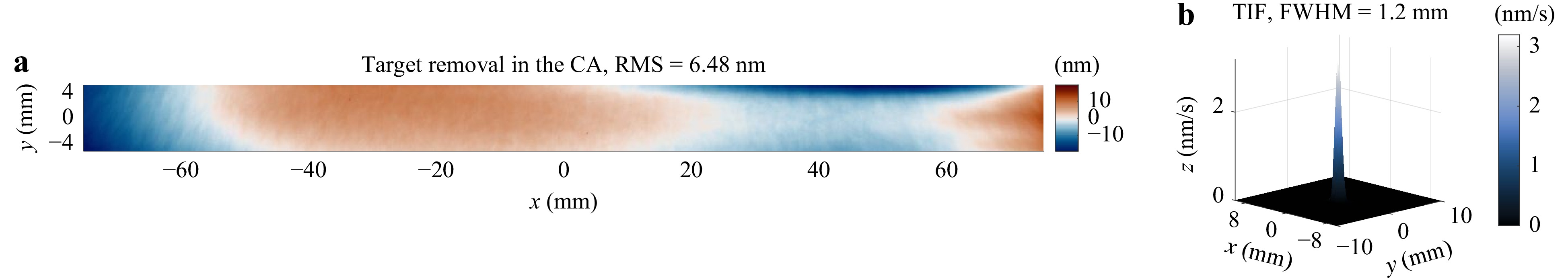
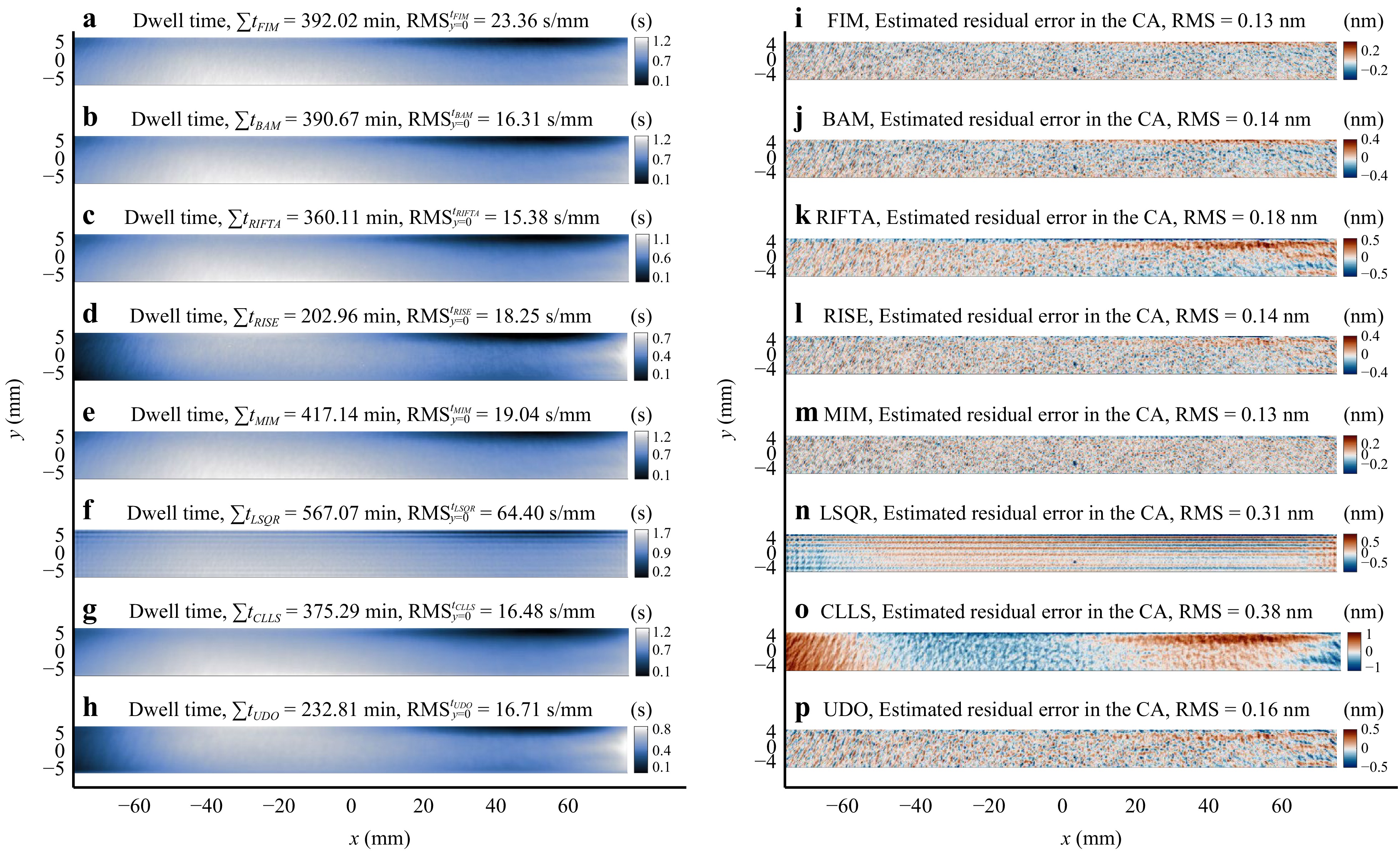
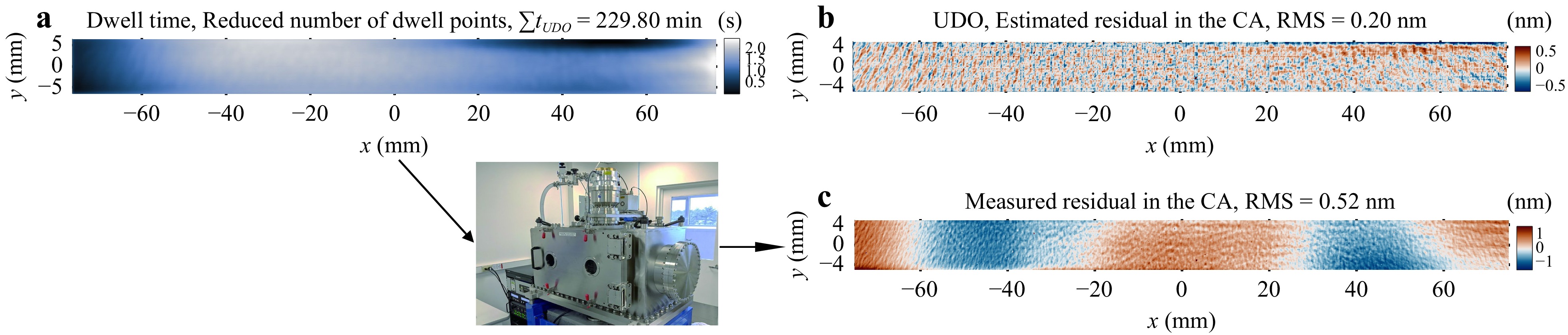
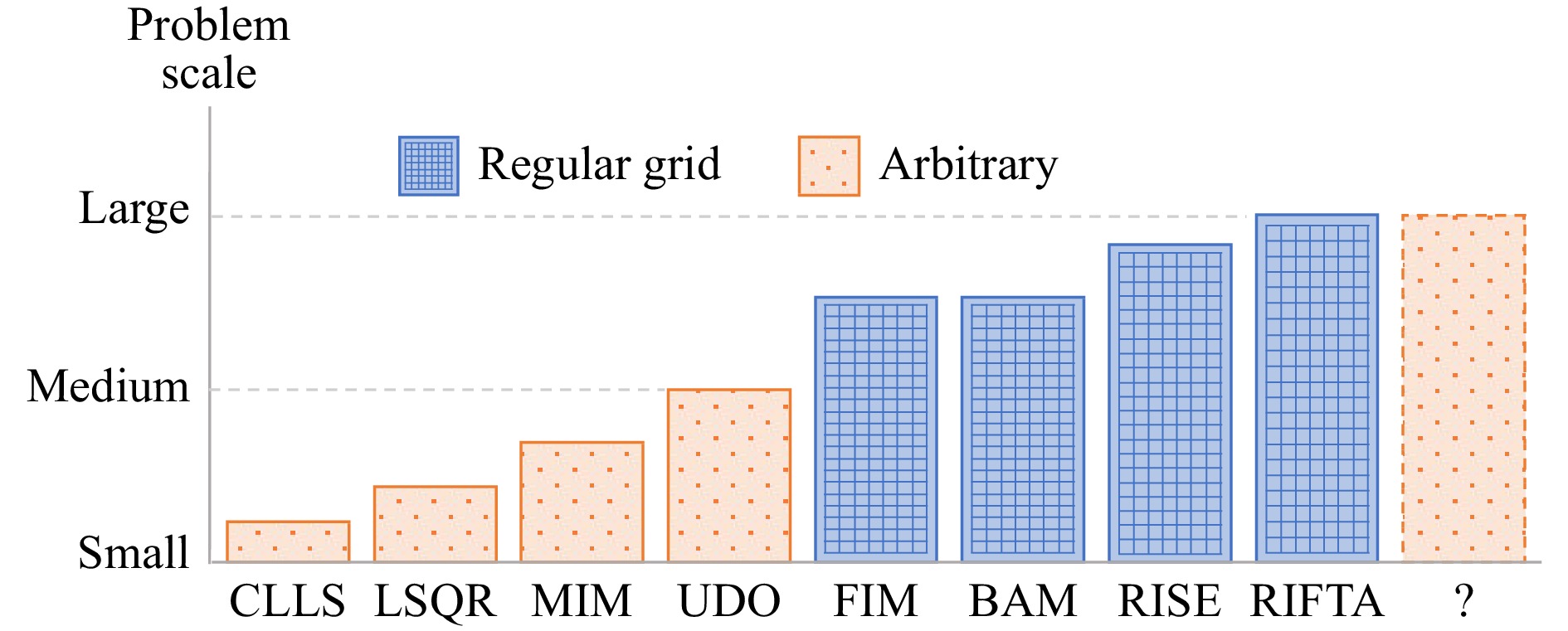
Dwell time plays a vital role in determining the accuracy and convergence of the computer-controlled optical surfacing process. However, optimizing dwell time presents a challenge due to its ill-posed nature, resulting in non-unique solutions. To address this issue, several well-known methods have emerged, including the iterative, Bayesian, Fourier transform, and matrix-form methods. Despite their independent development, these methods share common objectives, such as minimizing residual errors, ensuring dwell time's positivity and smoothness, minimizing total processing time, and enabling flexible dwell positions. This paper aims to comprehensively review the existing dwell time optimization methods, explore their interrelationships, provide insights for their effective implementations, evaluate their performances, and ultimately propose a unified dwell time optimization methodology.
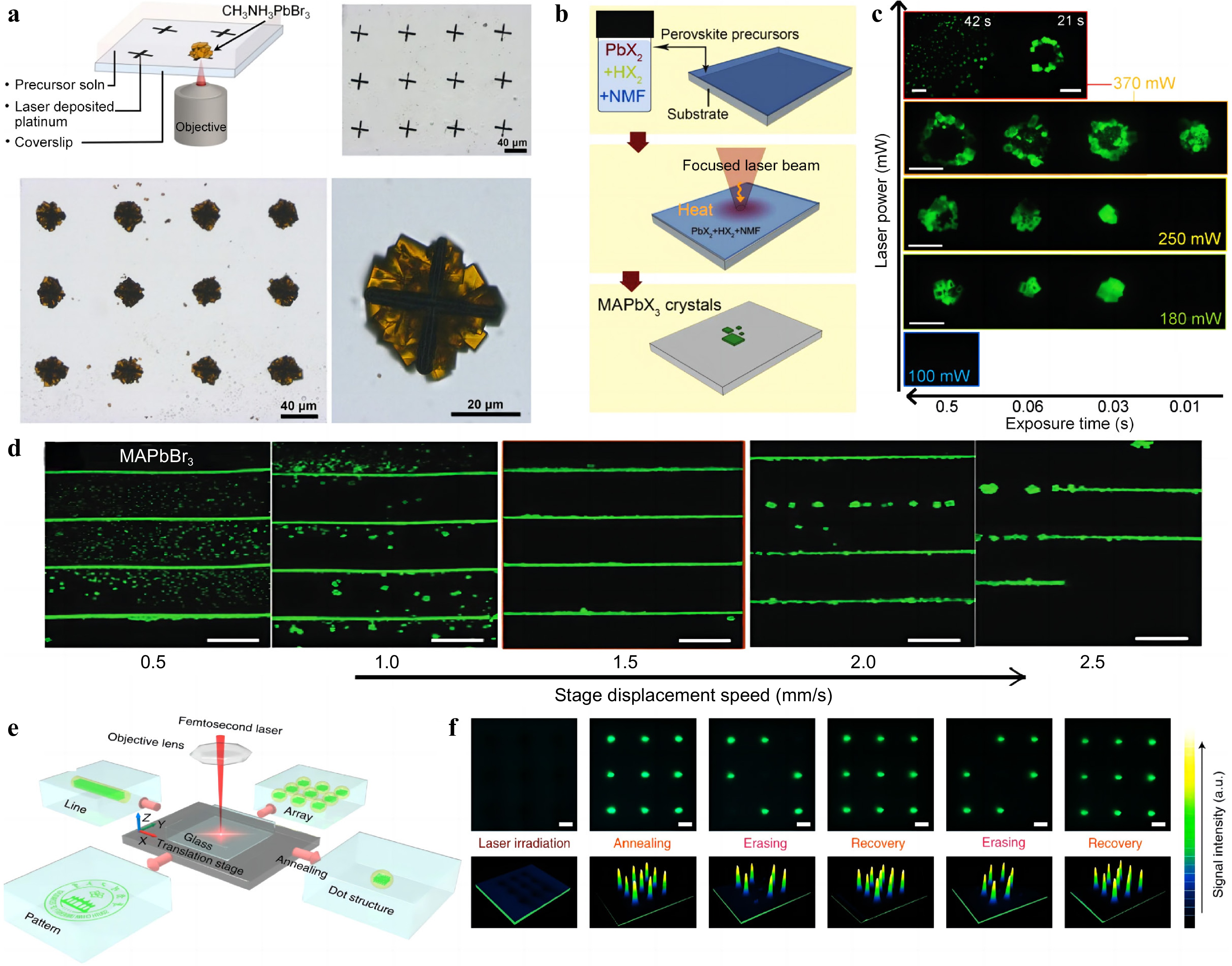
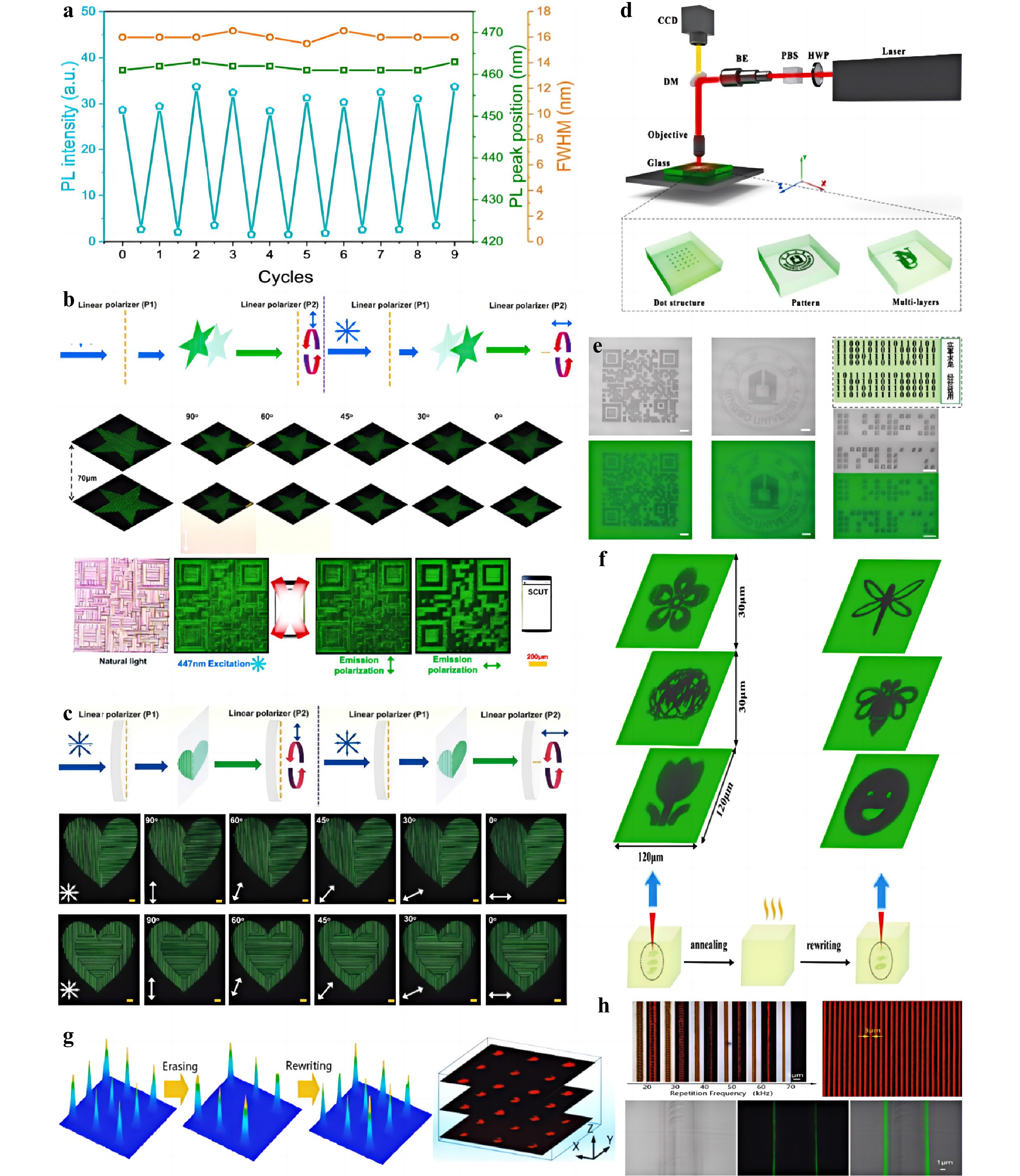
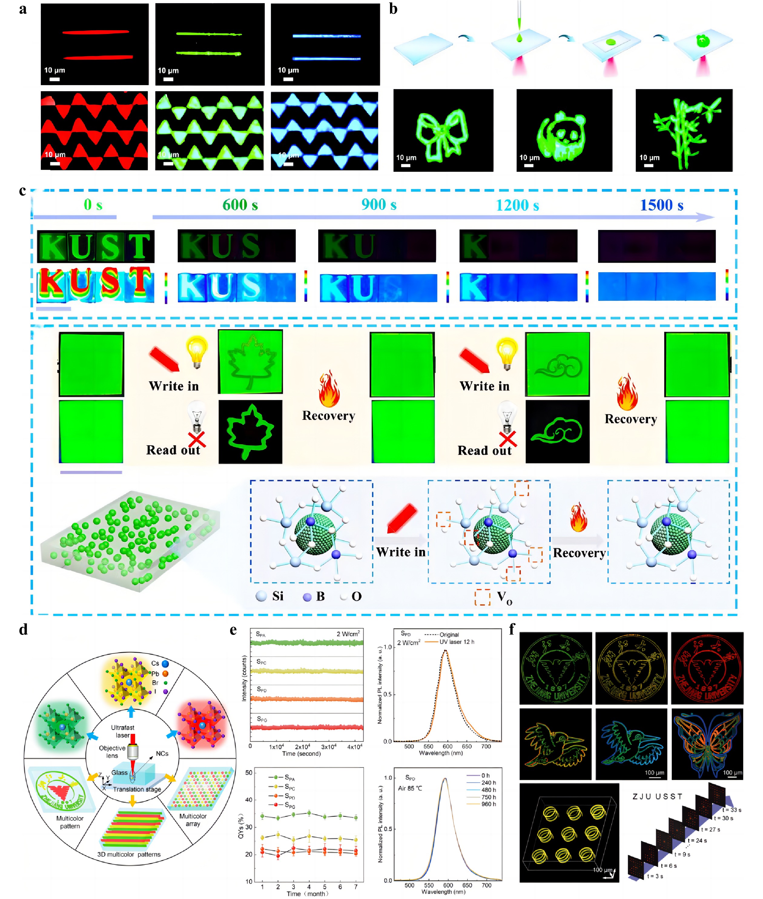
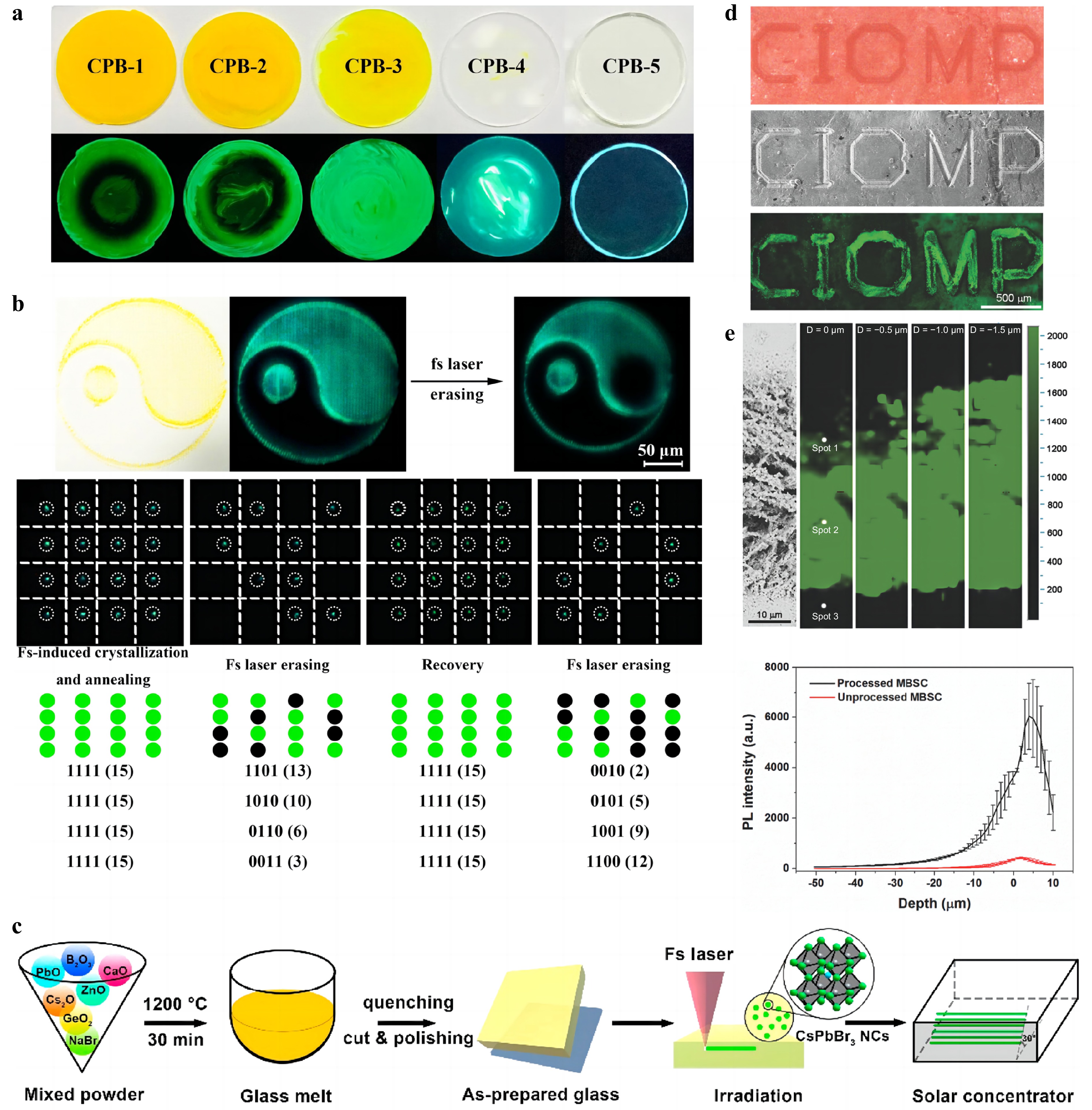
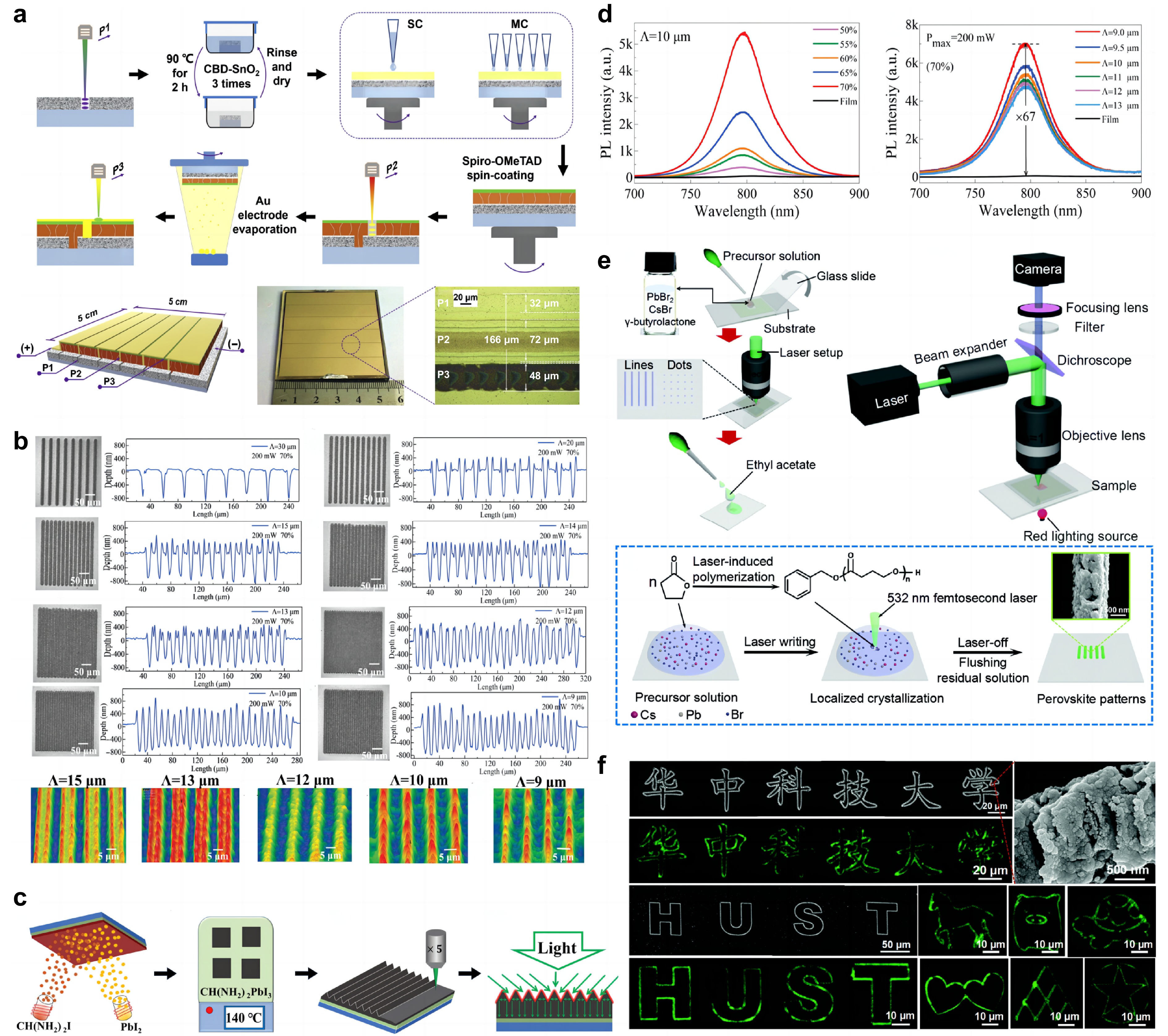
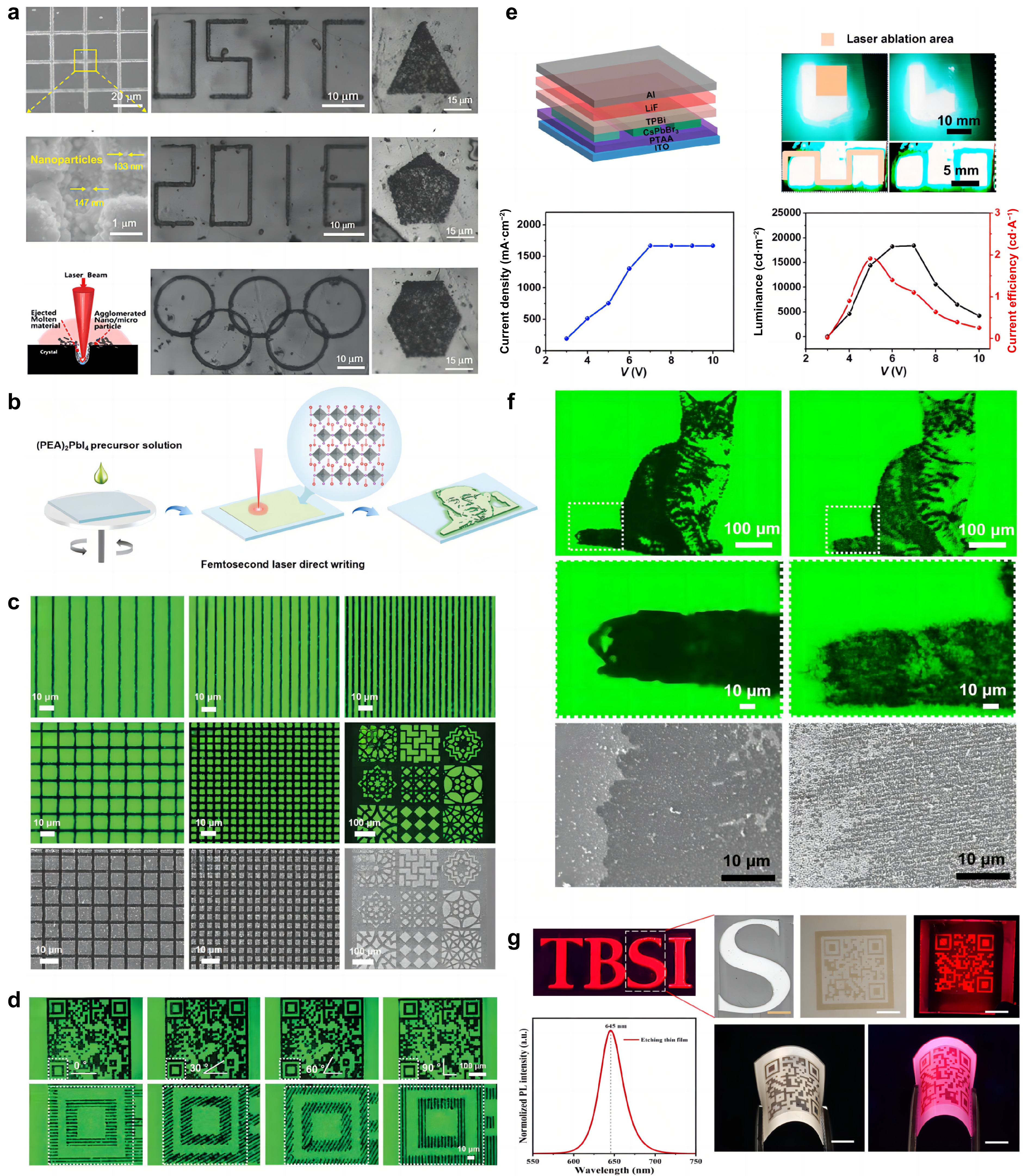
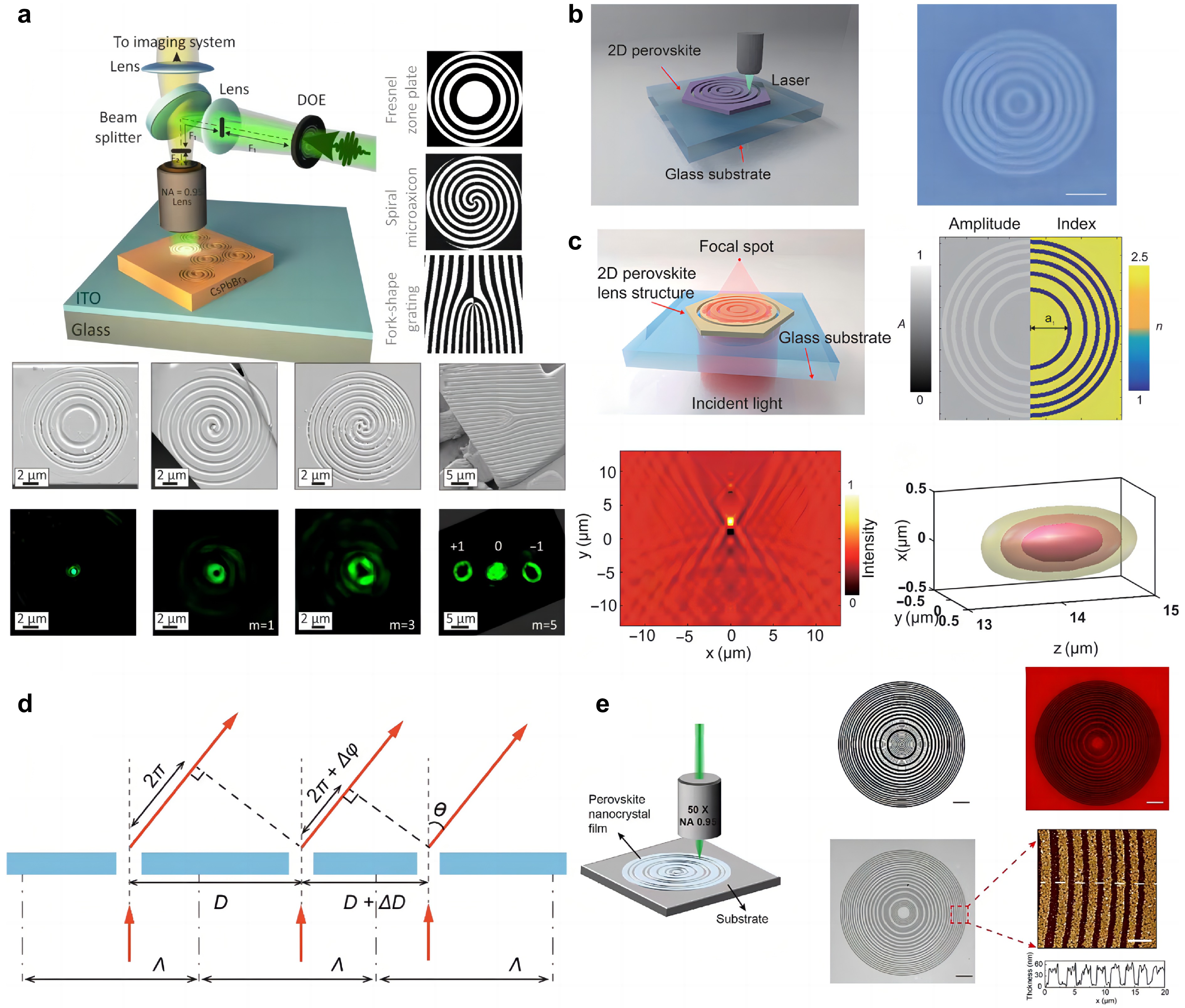
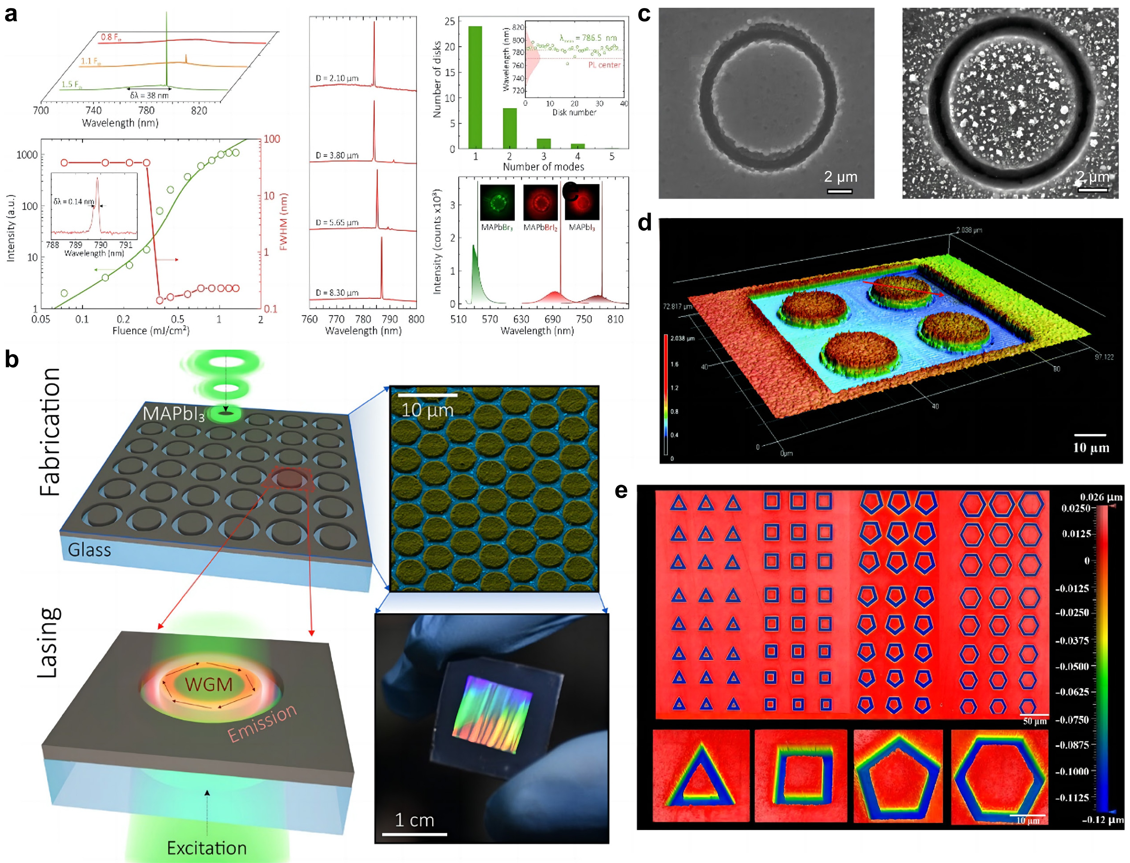
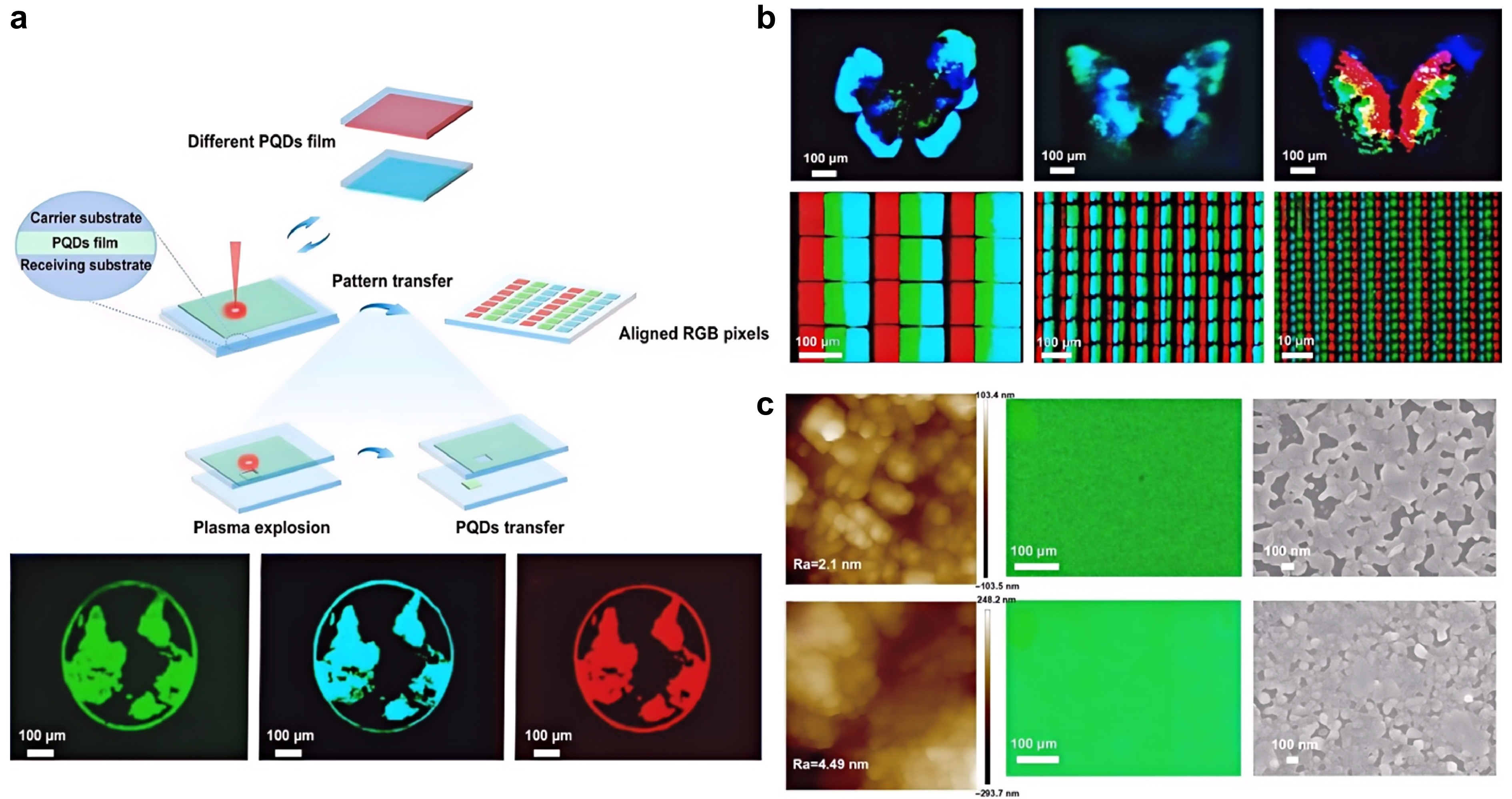
Perovskite materials have become a popular research topic because of their unique optical and electrical properties, that enable extensive applications in information storage, lasers, anti-counterfeiting, and planar lenses. However, the success of the application depends on accomplishing high-precision and high-quality perovskite patterning technology. Numerous methods have been proposed for perovskite production, including, a femtosecond laser with an ultrashort pulse width and ultrahigh peak power with unique advantages such as high precision and efficiency, nonlinearity, and excellent material adaptability in perovskite material processing. Furthermore, femtosecond lasers can induce precipitation of perovskite inside glass/crystals, which markedly enhances the stability of perovskite materials and promotes their application and development in various fields. This review introduces perovskite precipitation and processing via femtosecond lasers. The methods involved and advantages of femtosecond-laser-induced perovskite precipitation and patterning are systematically summarized. The review also provides an outlook for further optimization and improvement of femtosecond laser preparation and processing methods for perovskites, which may offer significant support for future research and applications of perovskite materials.


 Email
Email RSS
RSS