-
Micro-light-emitting diode (micro-LED) display technology holds significant promise for a wide range of consumer and commercial applications, such as augmented and virtual reality headsets, smartwatches, and next-generation mobile devices. These displays offer many advantages over traditional display technologies, such as LCD and OLED, boasting higher brightness, improved contrast, and very small pixel size, making them an attractive choice for compact, high-resolution displays1,2. A significant challenge in developing micro-LED displays is the miniaturization of individual LED elements. The term micro-LED typically refers to LEDs with dimensions smaller than 100 μm3. The dominant technology for assembling a full-color LED display, known as pick-and-place, involves integrating LEDs from three separate substrates, each optimized for a specific color wavelength. This approach allows for the precise engineering of the active regions to achieve optimal performance for red, green, and blue emitters. However, transferring and assembling these microscopic LED chips onto a display backplane is intricate and resource-intensive, posing limitations on the resulting displays’ achievable resolution, yield, and cost-effectiveness4. Fluidic self-assembly has been explored to circumvent this manufacturing challenge, and recent work demonstrated the self-assembly of more than 19 000 gallium-nitride (GaN) chiplets 45 µm in diameter in a research setting5.
Integrating a photoluminescent color-converting film onto blue LEDs is a widely used approach for display colorization, which avoids the technical challenges of mass transfer methods6. This approach takes advantage of the superior luminous efficiency and manufacturing maturity of blue GaN LEDs. Every display pixel comprises three blue sub-pixels, two encapsulated by a red or green color-converting layer. Rare-earth phosphors are widely used for photoluminescent color conversion; their large particle size inhibits their uniform coating on micro-LEDs7. Quantum dots (QDs) have garnered significant attention as a color-conversion material due to their exceptional optical properties, including narrow emission line widths, high quantum yields, small particle size, and solution processability8,9. A precise and efficient method for fabricating QD pixel arrays with dimensions less than 100 μm is needed to meet the industry demands for high-resolution, high-brightness, and high-efficiency displays10. Traditional approaches to fabricating QD color converters for micro-LED displays have faced several limitations. Conventional QD pattern methods include transfer printing, inkjet printing, and photolithography10,11. Transfer printing methods involve assembling the QD material into an organized pattern on a master transfer substrate and then transferring the patterned layer to the final substrate12,13. The main benefits of transfer printing methods are their potential for achieving high-resolution (sub-micron)12, efficient mass transfer, and scalability, but the requirement of a pre-structured master can reduce the flexibility of the process. Achieving a high-accuracy alignment between the stamp and the final substrate is also challenging. Unlike transfer printing methods, the photolithography-based method proposed in this paper achieves a high resolution (1 μm) while maintaining flexibility and efficient scalability. Inkjet printing (IJP) techniques have been employed to pattern QD films selectively. The QD films are deposited directly by piezoelectric nozzles in the print head, which ejects droplets of QD solution. The IJP methods are highly controllable, material efficient, and flexible; however, there are challenges in achieving small resolution, precise alignment, and uniform film thickness, which can impact display performance and yield14–17. Electrohydrodynamic printing (EHDP) utilizes conductive nozzles and substrates as electrodes to generate an electric field that carefully guides the ink droplets to the desired locations18. EHDP can reduce the resolution limit of inkjet printing from ~10 μm to less than 1 μm19, However, EHDP requires a conductive substrate, and the electric field may cause side effects on certain inks20. The thickness of printed films is usually limited21. The proposed method discussed below achieves higher resolution compared to printing methods while still maintaining the versatility to pattern solution-processed materials. Photolithography, a widely employed technique in the semiconductor industry, can achieve high-resolution patterns, but it is not well-suited for patterning QD materials due to its sensitivity to the harsh chemicals involved in the process22,23. Direct photolithography using QD-filled photoresists has been explored, but the photoresist chemistry typically must be designed for specific QDs. Mixing the QD directly into photoresist often reduces efficiency, degrades optical properties, and can impose other limitations on the functionality of the film. However, recent innovations in the photolithographic process have shown promise11,22,24-26. Photolithography based on photochemical mechanisms like ligand exchange typically reduces the efficiency of QDs due to surface defect generation during the process25. Recently, Qie et al. showed that QDs can be confined in a semiconductor polymer network frame using a ligand cross-linking mechanism to form high-quality patterns27.
Our group previously developed a photolithography-based process for patterning solution-processed perovskite films utilizing a dry mechanical lift-off technique28. This method combines the scalability and high-resolution capabilities of photolithography with the versatility of patterning solution-processed materials while preserving their optical properties, making it highly desirable. A similar process was applied later to pattern CdSe/CdZnSe QDs and achieved resolution down to 5 μm29. In this paper, we present further advancements of this method, demonstrating the process at a wafer scale with the highest pattern resolution of ~1 μm. Additionally, we show the universal potential of this technique by demonstrating compatibility with green perovskite QDs and red CdSe/ZnS core-shell QDs. We also achieved integration with a typical LED substrate by applying this method to micro-pattern QDs directly onto a blue GaN LED array.
-
The principle of the dry lift-off micro-patterning process is illustrated in Fig. 1. A clean substrate is coated with a buffer layer via chemical-vapor deposition (CVD). Currently, this process leverages the limited adhesion of parylene to various substrates and utilizes it as the buffer layer. A typical photolithography process is used to show the pattern on the substrate. The pattern is then transferred onto the buffer layer using plasma etching. Subsequently, QDs are deposited on the substrate, and the buffer layer is mechanically peeled off, leaving behind the patterned QDs. In general, this method can pattern any solution-processed material and can be repeated for full-color displays. This method also allows for QD recycling by dissolving the peeled-off layer in QD solvent, which is an added benefit in the manufacturing process. Details of this method are further discussed in the Supplementary Information.

Fig. 1 Diagram depicting the photolithography-based dry lift-off method for micro-patterning of multiple solution-processed films on a single substrate.
A wafer-scale processing of this method is necessary to validate its compatibility with standard semiconductor fabrication processes. In this study, we used a 4-inch glass wafer as the substrate and CsPbBr3 perovskite QDs (PQDs) as the green color converter material for the pattern. The PQDs were synthesized at room temperature using the ligand-assisted reprecipitation (LARP) method with triple-ligands30,31. Although many methods exist for synthesizing PQDs, a room-temperature strategy is adopted due to its minimal requirements for environmental control factors such as temperature and inert gas conditions. The synthesis and characterization of PQDs are further discussed in the Supplementary Information.
The triple-ligand-coated CsPbBr3 PQDs morphology was analyzed using transmission electron microscopy (TEM) and high-resolution TEM (HRTEM) images. The CsPbBr3 PQDs colloidal solution was drop-casted onto a lacey carbon grid for analysis. Supplementary Figure 1a shows the TEM image displaying square-shaped PQDs in a two-dimensional view. Based on symmetry, we can infer that the actual PQDs likely have a cubic-like shape in three dimensions. The bright regions between the dots are also distinct and continuous, suggesting a dense layer of surface ligands on the PQD surfaces. This dense coverage effectively prevents direct aggregation of the PQDs. The HRTEM image of a single PQD is shown in the upper-right inset of Supplementary Figure 1a. This revealed a highly ordered crystalline lattice throughout the perovskite region. The measured interplanar distance between crystal planes is 0.58 nm, consistent with prior work31. The lower-right inset of Supplementary Figure 1a shows the particle size distribution histogram of the PQDs, which reveals an average edge length of 11 ± 1.2 nm.
The photoluminescence (PL) spectrum of the CsPbBr3 PQD thin film exhibited an intense and narrow symmetric peak at 517 nm in the green region with a full-width half-maximum of 19.5 nm, as shown in Supplementary Figure 1b. The CsPbBr3 PQDs achieved a PL quantum yield (PLQY) of 93.6% (Supplementary Figure 1c), indicating that the triple-ligands effectively passivate the PQDs. The Time-Resolved PL (TRPL) was measured for the CsPbBr3 PQDs to examine the exciton recombination dynamics. The TRPL curve shows exponential decay and is fitted to the bi-exponential decay function (Supplementary Figure 1d), given in Eq. 1. The average lifetime was calculated using Eq. 232,33.
$$ y(t)=A_1 \exp(-t/\tau_1)+A_2 \exp(-t/\tau_2) $$ (1) $$ {\tau }_{\mathrm{a}\mathrm{v}\mathrm{e}}={(A}_{1}{\tau }_{1}^{2}+{A}_{2}{\tau }_{2}^{2})/({A}_{1}{\tau }_{1}+{A}_{2}{\tau }_{2})$$ (2) Here, t represents time, A1 and A2 are weighing parameters, which contribute to the decay components, t represents time, τ1 and τ2 correspond to trap-assisted nonradiative recombination and free-charge carrier radiative recombination, respectively. After bi-exponential decay fitting, the estimated decay components τ1 and τ2 are 13.54 ns and 35.95 ns, respectively. The average decay time for CsPbBr3 PQDs from the parameters obtained by the bi-exponential fit is 17.25 ns. The high PLQY and long lifetimes are attributed to the self-passivation effect due to the abundance of Br precursor during synthesis, which creates a high Br environment while suppressing surface defects. The synthesized CsPbBr3 PQDs are utilized in our demonstration of single-color and multi-color displays.
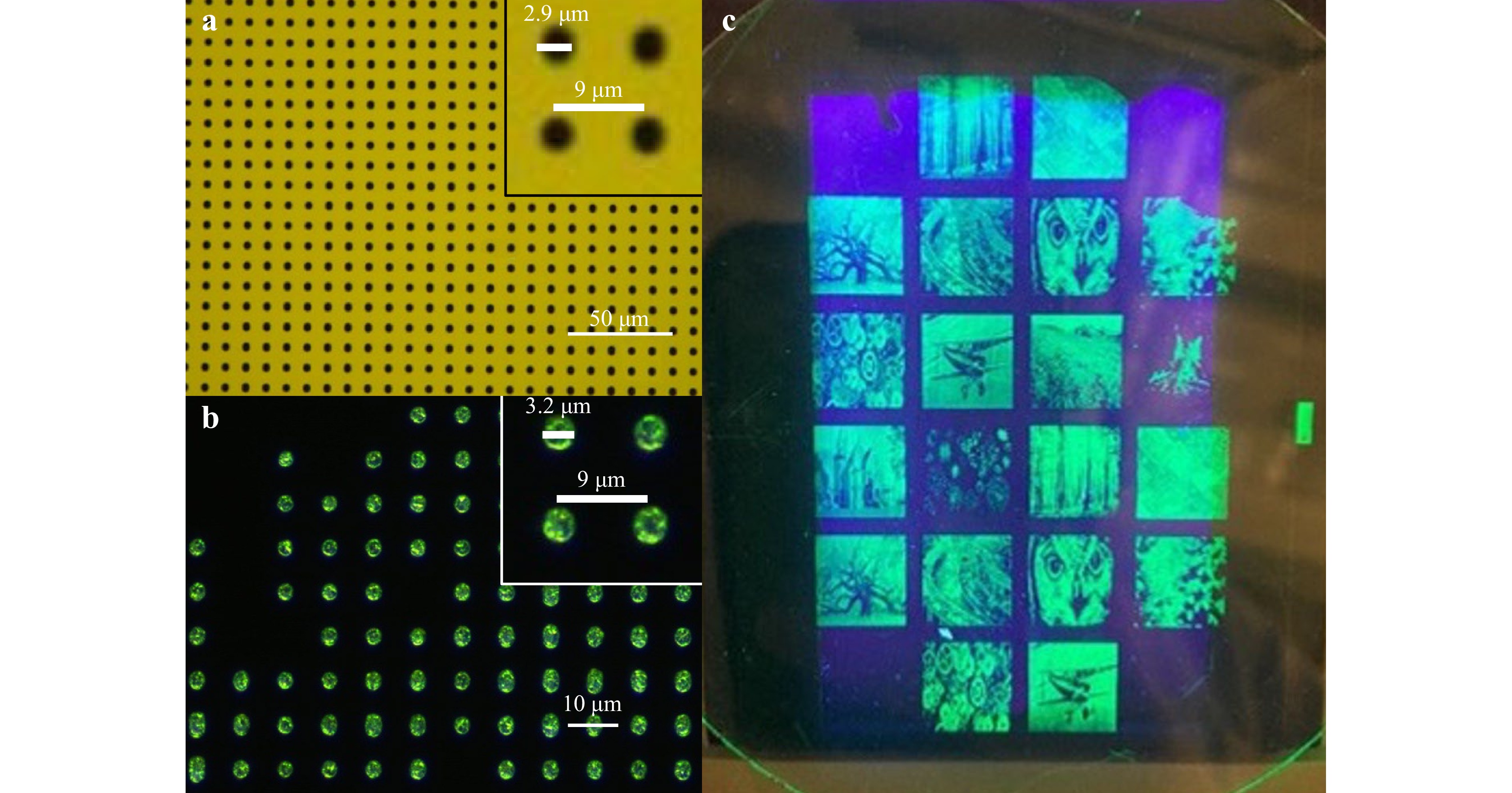
The process depicted in Fig. 1 was used to pattern the glass wafer with a mask featuring various pixel sizes ranging from 1 to 10 µm. Fig. 2a shows an optical microscope image of the wafer after the photoresist has been developed. The patterns are then transferred to the parylene layer, and PQDs are deposited by drop-casting. This method involves dispensing a solution containing PQDs onto the substrate, allowing it to spread and form a thin film. The buffer parylene layer is then mechanically peeled away, leaving the desired PQD patterned films on the wafer. This step is critical as it ensures that the PQDs are precisely patterned without any additional processing that could potentially alter their properties. Under a UV lamp, the bright green photoluminescence of the fabricated pixels is visible under a fluorescence microscope (Fig. 2b). The entire glass wafer, featuring various images patterned with green PQDs under UV illumination, is shown in Fig. 2c. The static image is created by encoding image pixel intensities into the size of the QD features. By removing or varying the size of individual QD features, we can produce a high-resolution, high-contrast static images (Fig. 2c) from a uniform-intensity backlight. This intentional variation in pixel size can be seen more clearly in Fig. 4. Note that Fig. 2a corresponds to a different region of the wafer from Fig. 2b, with Fig. 2a showing uniformly populated pixels of the same size by design.

Fig. 2 a Optical microscope image of the photoresist layer after developing, the inset shows the zoom-in view of the developed features, b fluorescence microscope image of micro-patterned green PQD pixels, the inset shows the zoom-in view of patterned PQDs, and c glass wafer displaying different images patterned with green PQDs under a UV lamp.
The high-resolution images show the effectiveness of the dry lift-off process for patterning perovskites. The strong green luminescence and high color contrast observed in these patterns indicate the merits of this method in preserving the PQD optical quality and achieving clean patterns. The high resolution and uniformity of the patterns further highlight the precision of the technique.
To demonstrate the universal applicability of this method, commercially available red-emitting CdSe/ZnS core-shell QDs in toluene (Ocean NanoTech, QSR-620-50) were patterned on the substrate. As with the green PQDs, the red CdSe/ZnS QDs are patterned via the dry mechanical lift-off method. Following the deposition of red CdSe/ZnS QDs, the parylene layer is mechanically peeled off, revealing the desired pattern on the wafer (Fig. 3a-c). The bright red luminescence and clear pattern confirmed the successful dry lift-off process application for these QDs. The high color contrast and strong luminescence indicate that the QDs maintain their optical quality and performance after patterning.

Fig. 3 a Wafer after the pattern is developed on the substrate, the inset shows the zoom-in view of developed features, b optical microscope image of red CdSe/ZnS QDs patterned on the glass wafer showing feature size of 1.04 µm, and c fluorescence microscope image of patterned red CdSe/ZnS QDs, the inset shows the zoom-in view of patterned features.
Supplementary Figure 2a displays a detailed two-dimensional height profile of a 5 × 5 µm sample area obtained using atomic force microscopy (AFM). This technique offers high-resolution imaging of the sample’s surface topography, enabling precise measurement of surface features. Additionally, a cross-sectional height profile scanned along the vertical axis of this area is shown in Supplementary Figure 2b. This cross-sectional view highlights height variations across the sample, which are crucial for evaluating pattern uniformity and thickness. These measurements show that the QD color converter has an approximate width and height of 1.2 µm and 180 nm, respectively.
To achieve a full-color display, it is desirable to pattern green, red, and sometimes blue color converter pixels on a single substrate with a blue or UV backlight underneath. The blue or UV light is absorbed by the QD pixels, which re-emit green, red, or blue light via photoluminescence34–36. By repeating the described process, we successfully patterned green PQDs and red CdSe/ZnS QDs on the same substrate. The red QDs were patterned first on the wafer, using the dry lift-off method described previously. Subsequently, a new parylene layer was deposited on top of the patterned red QDs. This step is crucial as it provides a fresh surface for the subsequent patterning of green PQDs while simultaneously protecting the previously patterned QDs. The same photolithography and etching processes were then applied to the new parylene layer to create the pattern for the green PQDs. The green PQDs were deposited onto the substrate, and the parylene layer was peeled off, revealing the green QD pattern integrated with the previously patterned red QDs. The wafer now features red and green QDs patterned on the same substrate, demonstrating the two-color patterning capability of this method. Fig. 4 depicts fluorescence microscope images of the patterned two-color arrays. The smallest feature size achieved was approximately 2 µm, indicating the high resolution and precision of the patterning process. This successful multi-color patterning demonstrates the versatility and effectiveness of the dry lift-off method for creating complex, high-resolution patterns with QDs of vastly different types.

Fig. 4 a Fluorescence microscope image of multi-color patterns integrating green perovskite QDs and red CdSe/ZnS QDs using the dry lift-off method, and b enlarged image of the multi-color pattern.
To validate that our patterning process can be applied to a micro-LED backplane, we acquired commercially available GaN/AlGaN epitaxial wafers on sapphire substrates (from University Wafer) and fabricated large-size blue LED arrays. The epitaxial wafer structure consists of an active quantum well region sandwiched between n-type GaN/AlGaN layers at the bottom and p-type GaN/AlGaN layers at the top. The quantum well region consists of 10 alternating sub-layers of InGaN (3.5 nm) and GaN (5 nm). This specific structure is designed to optimize the emission efficiency and wavelength of the blue LEDs. The fabrication process of the blue LEDs began with etching the wafer down to the heavily doped n-type GaN layer. This step is crucial for defining the individual LED pixels and ensuring proper electrical isolation. Following the etching, an oxide layer was deposited to passivate the etched sidewalls of the structure, which helps prevent leakage currents and improve the reliability of the device. Next, contact windows were opened through the oxide layer using dry etching techniques. These windows are essential for establishing electrical connections between the underlying layers. Finally, the electrical contacts to the top p-type GaN/AlGaN layer and the bottom n-type GaN layer were completed through metal deposition. This step involves depositing metal layers to form the anode and cathode contacts, ensuring efficient current injection into the LEDs. Fig. 5 shows an image of the fabricated 4 × 4 blue LED array on a chip area of 1 cm × 1 cm and another image of one of the LEDs turned on under a forward bias. The observed bright blue emission confirms the successful operation of the fabricated LEDs and validates the quality of the epitaxial layers and the effectiveness of the electrical contacts.

Fig. 5 Blue backlight LED array. a The fabricated 4 x 4 InGaN/GaN blue LED array on a sapphire substrate, and b the same sample with one of the blue LEDs turned on.
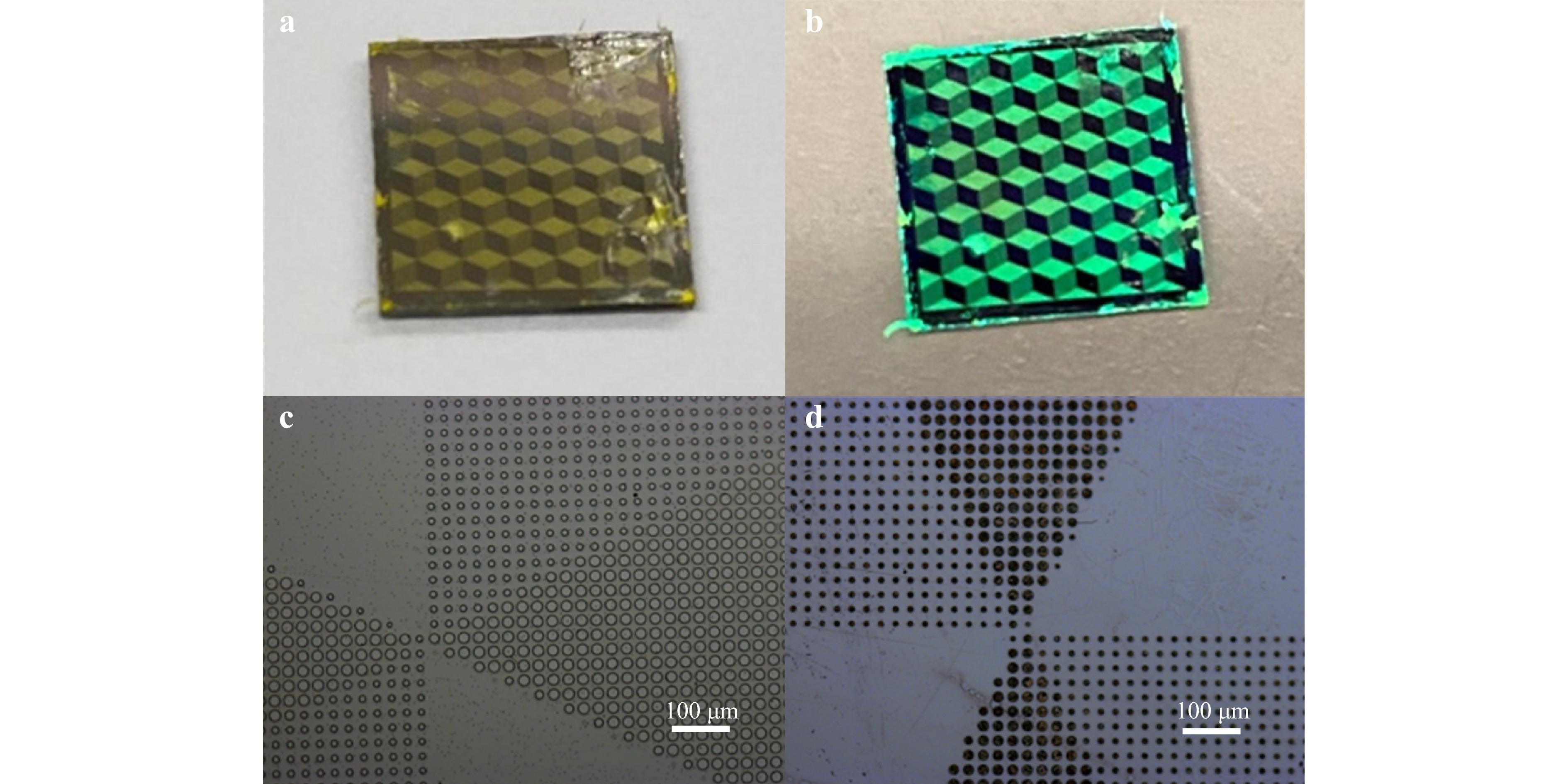
Prior to the parylene deposition step in the dry lift-off method, an aluminum black-matrix layer is deposited on the sapphire substrate. The patterns were transferred to both the parylene and aluminum layers during etching. Green PQDs were deposited and patterned on this substrate of blue LEDs through mechanical dry lift-off. Fig. 6a shows a photograph of PQDs patterned on the sapphire substrate of a blue LED array chip, and Fig. 6b shows the fluorescence of the PQDs under UV excitation. Fig. 6c shows the close-up optical microscope image of the patterned parylene-C layer. Fig. 6d shows the patterned PQDs after depositing the PQDs and lifting off the parylene-C layer. The aluminum layer covers the region without PQDs. The results show that PQDs were patterned on the blue LED substrate with good uniformity using parylene-C-mediated dry lift-off photolithography.

Fig. 6 PQD color converters integrated with a blue LED backlight. Images of a PQDs patterned on the sapphire substrate of the blue LED array chip, and b fluorescence of the green-emitting PQDs under UV excitation. Optical microscope images of c the patterned parylene layer on top of aluminum black-matrix, and d patterned PQDs after depositing the PQDs and lifting off the parylene layer.
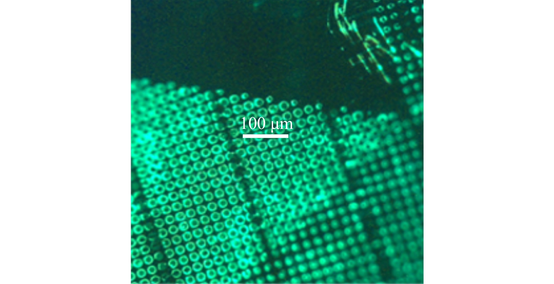
The LED chip covered with patterned PQDs was placed under a fluorescence microscope, and one of the blue backlight LEDs was turned on (Fig. 7). Part of the image is out of focus because the wires connected to the backside electrodes of the blue LED array force the sample to be slightly tilted under the microscope. The aluminum layer patterned simultaneously with the parylene-C layer served as a black-matrix layer between QDs and blocked the blue backlight coming through the area without QD coverage. These results demonstrate the compatibility of our micro-patterning method with micro-LED display manufacturing.
-
The results demonstrate a high-resolution, large-area photolithographic approach for patterning QD color converter thin films with parylene as an intermediate. Parylene facilitates a dry lift-off procedure in which undesired QDs are mechanically removed without the use of additional solvents. We achieved a pattern resolution close to 1 µm, which is limited by the capability of the equipment in the Washington Nanofabrication Facility.
Since the QDs are deposited as the final step and do not undergo any further processing, their PL properties and narrow linewidth are preserved. This ensures that the QDs retain high performance and optical quality, making this technique highly attractive for applications requiring precise and reliable patterning of solution-processed materials. Additionally, preserving the optical properties of QDs is crucial for their use in optoelectronic devices, where consistent performance and efficiency are essential.
This method has been successfully used to create single- and multicolor patterns. The parylene coatings effectively shield the underlying QD films, allowing for the creation of multicolor converter patterns through repeated use of the usual photolithography technique. Furthermore, since the method is agnostic to the materials to be patterned, QDs of different types can be integrated, which was demonstrated by the successful integration of green PQDs with red CdSe/ZnS QDs. The display industry has yet to reach a consensus on the optimum QDs. InP QDs are appealing for being non-toxic, and their optical quality has improved37. The universality of the dry lift-off micro-patterning method can ensure agile adaptation to any adopted materials.
Our results demonstrate the versatility of this method for high-resolution micro-patterned solution-processed materials. Its simplicity and effectiveness also make it a promising approach for large-scale manufacturing and integration of QD-based devices, potentially lowering production costs and increasing accessibility for various applications.
-
This work is supported by the National Science Foundation (Award No. IIP-2140788), the University of Washington CoMotion Innovation Gap Fund, and the Washington Research Foundation. Part of material synthesis and characterization was supported by the National Science Foundation through Award No. CMMI-2227285 and the Science and Technology Center (STC) for Integration of Modern Optoelectronic Materials on Demand (IMOD) under Award No. DMR-2019444. Part of device fabrication was conducted at the Washington Nanofabrication Facility, a National Nanotechnology Coordinated Infrastructure (NNCI) site at the University of Washington supported by the National Science Foundation (NSF) (grant NNCI-1542101). The AFM and TEM imaging were performed at the UW Molecular Analysis Facility, part of the NSF NNCI to coordinate nanoscale research and development activities across the United States and is supported by NNCI-2025489 and NNCI-1542101. The authors thank Rose Johnson and Ethan Keeler for their helpful discussion.
A universal high-resolution micro-patterning technique for solution-processed materials
- Light: Advanced Manufacturing , Article number: (2025)
- Received: 31 May 2024
- Revised: 14 December 2024
- Accepted: 05 January 2025 Published online: 19 March 2025
doi: https://doi.org/10.37188/lam.2025.015
Abstract: A universal method of micro-patterning thin quantum dot films is highly desired by industry to enable the integration of quantum dot materials with optoelectronic devices. Many of the methods reported so far, including specially engineered photoresist or ink-jet printing, are either of poor yield, resolution limited, difficult to scale for mass production, overly expensive, or sacrificing some optical quality of the quantum dots. In our previous work, we presented a dry photolithographic lift-off method for pixelization of solution-processed materials and demonstrated its application in patterning perovskite quantum dot pixels, 10 µm in diameter, to construct a static micro-display. This report presents further development of this method and demonstrates high-resolution patterning (~1 µm diameter), full-scale processing on a 100 mm wafer, and multi-color integration of two different varieties of quantum dots. Perovskite and cadmium-selenide quantum dots were adopted for the experimentation, but the method can be applied to other types of solution-processed materials. We also demonstrate the viability of this method for constructing high-resolution micro-arrays of quantum dot color-convertors by fabricating patterned films directly on top of a blue gallium-nitride LED substrate. The green perovskite quantum dots used for fabrication were synthesized via the room-temperature ligand-assisted reprecipitation method developed by our research group, yielding a photoluminescent quantum yield of 93.6% and full-width half-maximum emission linewidth less than 20 nm. Our results demonstrate the viability of this method for use in scalable manufacturing of high-resolution micro-displays paving the way for improved optoelectronic applications.
Research Summary
Multicolor quantum dot micropatterning: Scalable manufacturing ready
The study presents a high-resolution photolithographic method for patterning quantum dot (QD) color converter films using parylene as an intermediary. This approach enables a dry lift-off process, mechanically removing unwanted QDs without solvents and achieving a resolution of approximately 1 µm. The deposited QDs maintain their photoluminescence properties and narrow linewidth, ensuring high performance and optical quality. This technique is ideal for precisely patterning solution-processed materials, which is crucial for optoelectronic devices. Single and multi-color patterns were successfully created by integrating different QD types, such as green PQDs and red CdSe/ZnS QDs. The versatility and simplicity of this method make it suitable for large-scale manufacturing, potentially reducing costs and enhancing the accessibility of QD-based applications.
Rights and permissions
Open Access This article is licensed under a Creative Commons Attribution 4.0 International License, which permits use, sharing, adaptation, distribution and reproduction in any medium or format, as long as you give appropriate credit to the original author(s) and the source, provide a link to the Creative Commons license, and indicate if changes were made. The images or other third party material in this article are included in the article′s Creative Commons license, unless indicated otherwise in a credit line to the material. If material is not included in the article′s Creative Commons license and your intended use is not permitted by statutory regulation or exceeds the permitted use, you will need to obtain permission directly from the copyright holder. To view a copy of this license, visit http://creativecommons.org/licenses/by/4.0/.


 DownLoad: