


-
Intense femtosecond (fs) laser pulses have shown great potential for directly forming periodic nanostructures with a period of 1/10 to 1/2 of the laser wavelength on solid surfaces via ablation1–16. These nanostructures have been successfully formed on various materials, including dielectrics1–9,13–16, semiconductors7,10,11, and metals12. Moreover, they can be formed on brittle materials such as glass13,15, and hard materials such as ceramics3,5,8,9,16 and sapphire7,14, making them useful for a wide range of applications such as reducing friction17, controlling wettability18, creating structurally coloured surfaces19, directing cell spreading20, and developing anti-reflection surfaces21. For industrial applications, such as metasurfaces for quantum photonics22, high-efficiency light-emitting devices, and high-sensitivity photodetectors23–25, achieving homogeneous nanostructures of consistent size over the entire surface and ensuring the quality of the nanostructures are crucial, as light scattering and energy loss caused by micrometre-scale defects can greatly degrade device performance. However, the formation of these structures is strongly dependent not only on the laser parameters such as the power, pulse width, and pulse number, but also on the target conditions such as the surface roughness and dielectric constant26,27. Therefore, consistently producing high-quality nanostructures with good uniformity over an entire surface is challenging.
An effective approach to form high-quality nanostructures is to monitor the formation of nanostructures in real time during fs laser-pulse irradiation and actively control the laser parameters to maintain a consistent formation. This method can also guarantee the homogeneity of the nanostructures throughout the laser-irradiation area. In such cases, an in-process monitoring technique is critical. However, because nanostructures are smaller than the wavelength of light, their morphologies cannot be directly observed using optical microscopy. Scanning electron microscopy (SEM) can be used for observations, although in-process observations remain difficult.
This study investigates the stable formation of line-like nanostructures with a constant period on glass irradiated with fs laser pulses utilising the real-time optical monitoring of nanostructure formation and feedback control of the laser power. We measured the reflectance and transmittance of a glass surface irradiated with fs pulses scanned in one direction and compared these measurements with the surface morphology observed using SEM. The results showed that surfaces with line-like periodic nanostructures exhibited decreased reflectance and significantly increased transmittance. These two measurements enabled the identification of the formation of nanostructures with a period of 200 nm and depth of 1 μm. Furthermore, by applying proportional-integral-derivative (PID) control to the laser power based on these specific values, we successfully reduced the defect ratio of the nanostructures over the entire irradiated area to ~2.4%, which was approximately ten times lower than that in the uncontrolled case.
-
We used focused fs laser pulses to create nanostructures on synthetic silica glass plates and measured the surface reflectance R and transmittance T. The power P of the laser pulses was adjusted to achieve the desired R and T as the nanostructures were formed. Fig. 1 shows a schematic of the optical configuration. A linearly polarised fs laser pulse from an ytterbium laser system was focused onto a synthetic silica-glass surface using an objective lens (OL). Here, P was controlled using an acousto-optic modulator. Light from two light-emitting devices (LED1, LED2) with different wavelengths was directed onto the laser-irradiated surface, and the light reflected and transmitted from the surface was detected using two cameras (C1 and C2). The microscopic images were acquired using a computer. The polarisation direction of the detected LED light was selected using a polariser (POL). The reflectance R = IR/IR0 and transmittance T = IT/IT0 were obtained from the reflected-light intensity IR and transmitted light intensity IT in the laser-irradiated area, respectively, where IR0 and IT0 are the reflected and transmitted light intensities in the non-laser-irradiated area, respectively. After laser irradiation, the surface morphology of the target was observed using SEM, and the relationship between R, T, and the surface morphology was investigated.
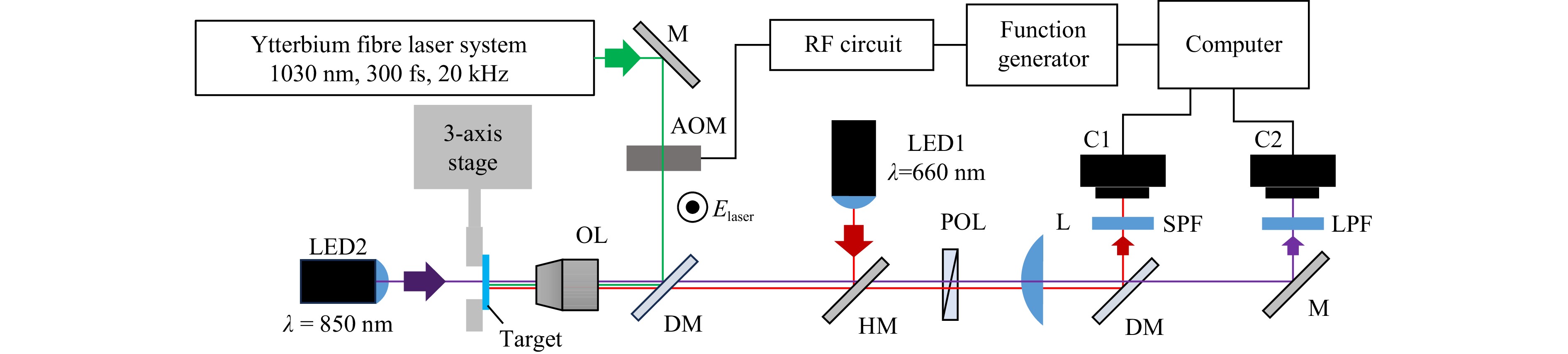
Fig. 1 Configuration of real-time monitoring and active feedback-control system for nanostructure formation on glass. AOM: acousto-optic modulator, M: mirror. DM: dichroic mirror, OL: objective lens, HM: half mirror, L: plano-convex lens, LED1, LED2: light emitting diodes, SPF: short-pass filter, LPF: long-pass filter, C1, C2: cameras. Elaser denotes the polarisation direction of the fs laser pulse. The polarisation direction of the observed LED light ELED was selected with a polariser (POL).
-
Fig. 2 shows an example of the R and T images along with an SEM image of the target surfaces irradiated with fs pulses at P = 7.5, 8.5, and 15 mW and a scanning speed of v = 1000 μm/s. Here, the polarisation directions of the fs pulse Elaser and LED light ELED were perpendicular to the scanning direction. At P = 7.5 mW, high-quality nanostructures with high linearity and a constant period of approximately 200 nm in the direction perpendicular to Elaser were formed, as shown in Fig. 2a. Cross-sectional observation showed that the groove depth is approximately 1 μm. The average R and T values for this surface were approximately 0.54 and 1.48, respectively, indicating a decrease in R and an increase in T. As shown in Fig. 2b, increasing P to 8.5 mW caused nanostructures to be formed at the bottom of the dimple; however, these nanostructures were inhomogeneous and had low linearity. The average R and T values for the surface were approximately 0.29 and 1.87, respectively, with R decreasing and T increasing more significantly than for the higher-quality nanostructures. As shown in Fig. 2c, a further increase in P to 15 mW led to a strong ablation of the laser-irradiated surface, and no periodic nanostructures were formed. The average R and T values were approximately 0.09 and 0.22, respectively, indicating a decrease in both R and T. Because the fs pulses with Elaser parallel to v formed line-like structures with their direction perpendicular to Elaser and v, and they had low linearity and were inhomogeneous, we focused on nanostructure formation induced by the fs pulses with Elaser perpendicular to v.
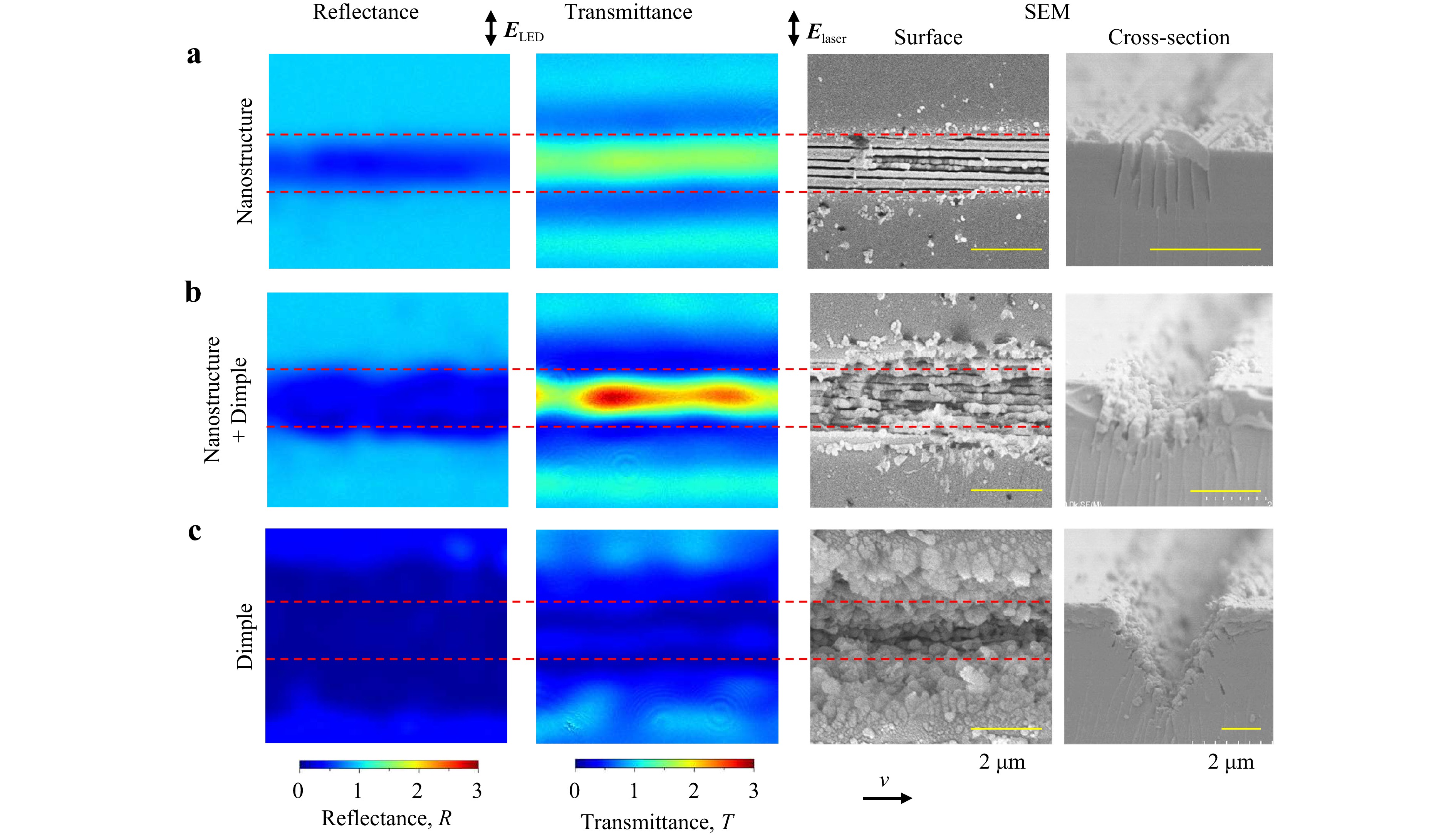
Fig. 2 Examples of reflectance (left), transmittance (middle), and SEM (right) images of surface and cross-section (right) of glass surfaces irradiated with fs laser pulses with a P = 7.5 mW, b P = 8.5 mW, and c P = 15 mW at v = 1000 μm/s. Elaser, ELED, and v denote the polarisation directions for the fs laser pulses and LED light and the scanning direction for the fs laser, respectively. The red dashed lines represent the laser-irradiated area for easier tracking. The yellow bars in the SEM images indicate 2 μm.
To investigate the relationship between R, T, and surface morphology, we measured both R and T for glass surfaces irradiated with fs pulses at P = 6.0–15 mW and v = 1–1000 μm/s, and acquired corresponding SEM images. ELED was set parallel or perpendicular to Elaser. From the obtained SEM images, we classified R and T into the three typical surface types shown in Fig. 2a-c. Fig. 3 shows R and T values averaged in the area of 2 × 2 μm, where the glass surface has structures formed by fs laser pulses with different P and v values. The surface shape was sensitive to the laser energy and scanning speed (i.e., pulse number), and the same type of surface had almost the same values of R and T when measured. The surface with the homogeneous nanostructures, shown in Fig. 2a, exhibited R = 0.6 ± 0.1 and T = 1.4 ± 0.1 for ELED parallel to Elaser, and R = 0.6 ± 0.1 and T = 1.2 ± 0.1 for ELED perpendicular to Elaser. The surface with the inhomogeneous nanostructures in the dimple, shown in Fig. 2b, exhibited R = 0.3 ± 0.1 and T = 1.5 ± 0.4 for ELED parallel to Elaser, and R = 0.3 ± 0.1 and T = 1.2 ± 0.3 for ELED perpendicular to Elaser. The surface with only the dimple, shown in Fig. 2c, exhibited R = 0.2 ± 0.03 and T = 0.4 ± 0.3 for ELED parallel to Elaser, and R = 0.2 ± 0.03 and T = 0.3 ± 0.1 for ELED perpendicular to Elaser. These findings indicate that the R and T values for the surface with homogeneous nanostructures differed from those for the other two surfaces and that these values depended on the surface shape. Moreover, changes in R and T were more pronounced when ELED was parallel to Elaser. Consequently, the formation of homogeneous nanostructures could be identified using the pair of R and T values. Setting the polarisation direction of the illumination light parallel to that of the fs laser pulses, which was perpendicular to the direction of the line-like structures, was effective for clearly identifying nanostructure formation.
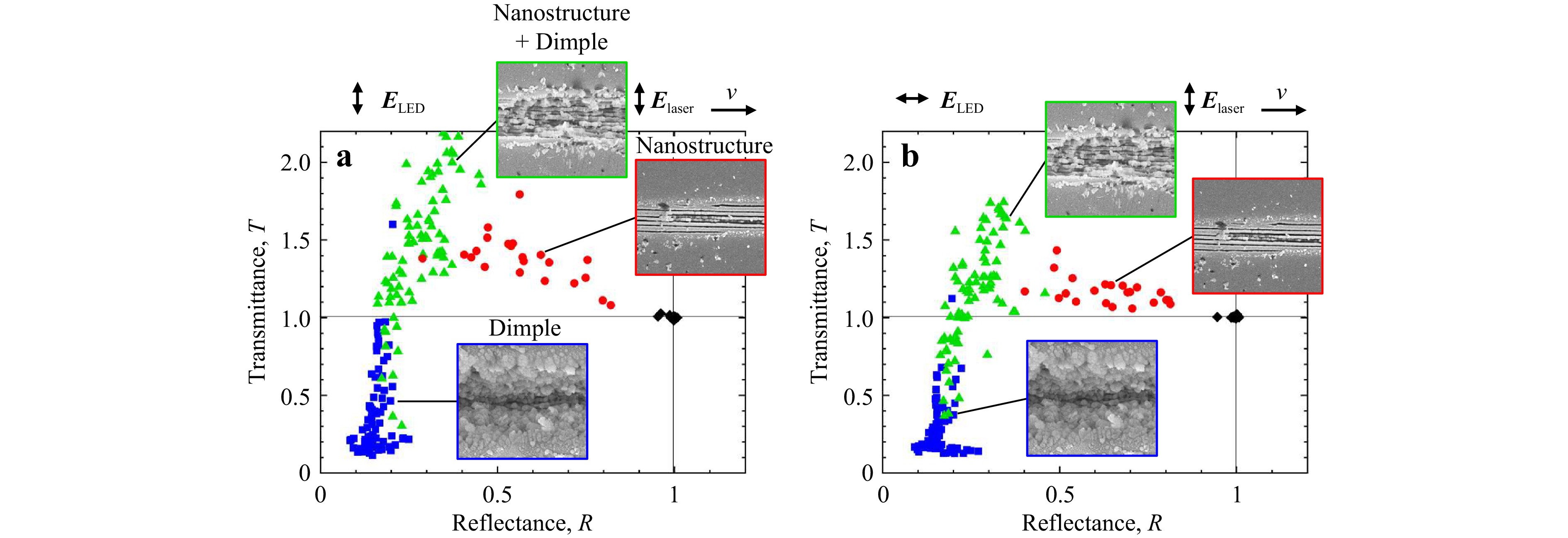
Fig. 3 Relationship between reflectance R, transmittance T, and morphology of glass surfaces irradiated with fs laser pulses of power P = 6.0–15 mW at scanning speed v = 1–1000 μm/s. The polarisation direction for the LED light ELED is a parallel and b perpendicular to the direction of laser polarisation Elaser. Elaser, ELED, and v denote the polarisation directions for the fs laser pulses and LED light and the scanning direction for the fs laser, respectively. Red circles, green triangles, and blue squares represent R and T for glass surfaces with homogenous nanostructures, inhomogeneous nanostructures in a dimple, and a dimple only, respectively. The insets denote examples of SEM images of these three typical surface types. Black diamonds denote measurements at non-irradiated surfaces.
-
We achieved the stable formation of homogeneous nanostructures on glass surfaces by employing PID control of the laser power P to maintain the desired setpoints for R and T measured in the process. Fig. 4 shows R, T, P, and an SEM image for the period t = 32–42 s after the initiation of irradiation (t = 0). Here, the scanning speed v was 10 μm/s, the scanning length was 1 mm, Elaser was parallel to ELED, and the desired setpoints for R and T were 0.9 and 1.3, respectively. The feedback rate was set to approximately 100 ms, which is the minimum time required for feedback. Details are described in the Materials and Methods section. As indicated in Fig. 4a, both R and T tended towards 1.0 during t = 37–39 s, after which, the nanostructures gradually ceased to form on the surface. As shown in Fig. 4b, P gradually increased to approximately 6.7 mW by t ≈ 39.5 s under PID control, leading to the formation of inhomogeneous nanostructures owing to strong ablation, as shown in Fig. 4c. At this point, R decreased to 0.7, while T increased considerably to 1.6. Subsequently, P decreased to approximately 6.6 mW by PID control, resulting in the stable formation of homogeneous nanostructures. These results indicate that in-process measurements of reflectance and transmittance may be useful in monitoring nanostructure formation and that regulating the laser power through feedback control can stably produce high-quality nanostructures.
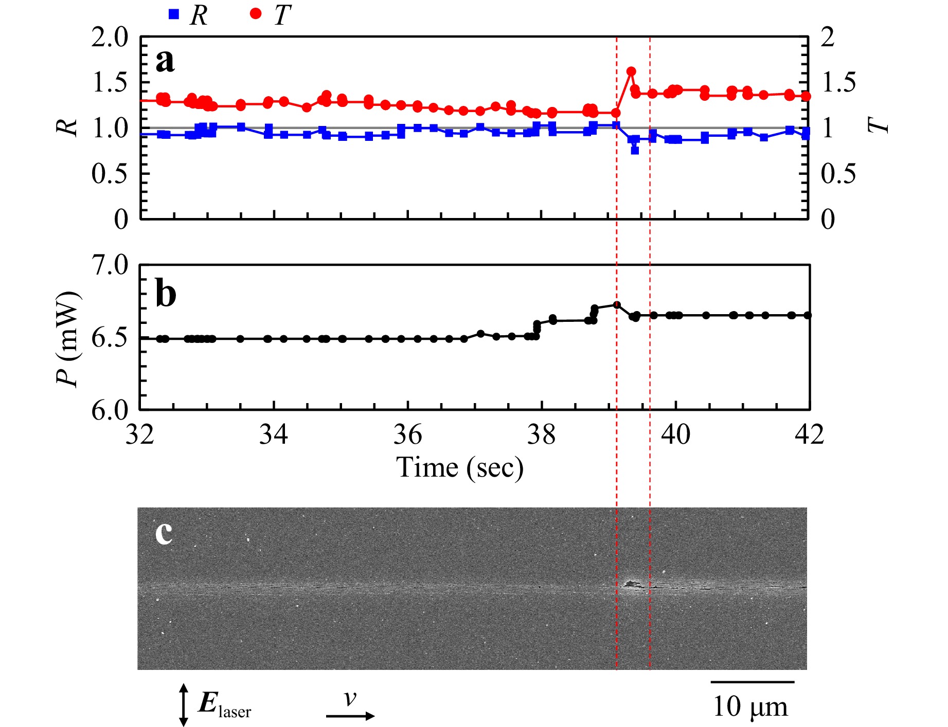
Fig. 4 a Reflectance R and transmittance T, b laser power P, and c SEM image of glass surfaces irradiated with fs laser pulses with P feedback-control by PID. For easy tracking, the red dashed lines represent the position of the irradiated surface and the time variations of R, T, and P. Elaser and v denote the polarisation direction for the fs laser pulses and the scanning direction, respectively.
We then compared the surface morphology of glass processed with and without the control to assess the effectiveness of the feedback control. Fig. 5a, b show SEM images of glass surfaces irradiated by fs laser pulses at a fixed power of P = 6.5 mW and a feedback-controlled power of P = 6.4–6.9 mW with the desired setpoints for R and T at 0.9 and 1.3, respectively. In both processes, the scanning speed v was 10 μm/s, scanning length was 1 mm, and polarisation direction for the fs pulses was parallel to that for the illumination light. Without the feedback control of P, the line-like nanostructures had many defects, particularly over longer distances. Conversely, with feedback control, the nanostructures were consistently formed in their entirety, with fewer defective areas. This improvement was due to the ability of the feedback control system to adjust the laser power P immediately upon defect detection. We conducted irradiation experiments ten times each, with and without the feedback control of P, and calculated the average value of the defect ratio across the entire irradiation area of the fs laser. The results showed defect ratios of 24.4% without feedback control and 2.4% with feedback control, which effectively reduced the defect ratio by a factor of approximately 10.
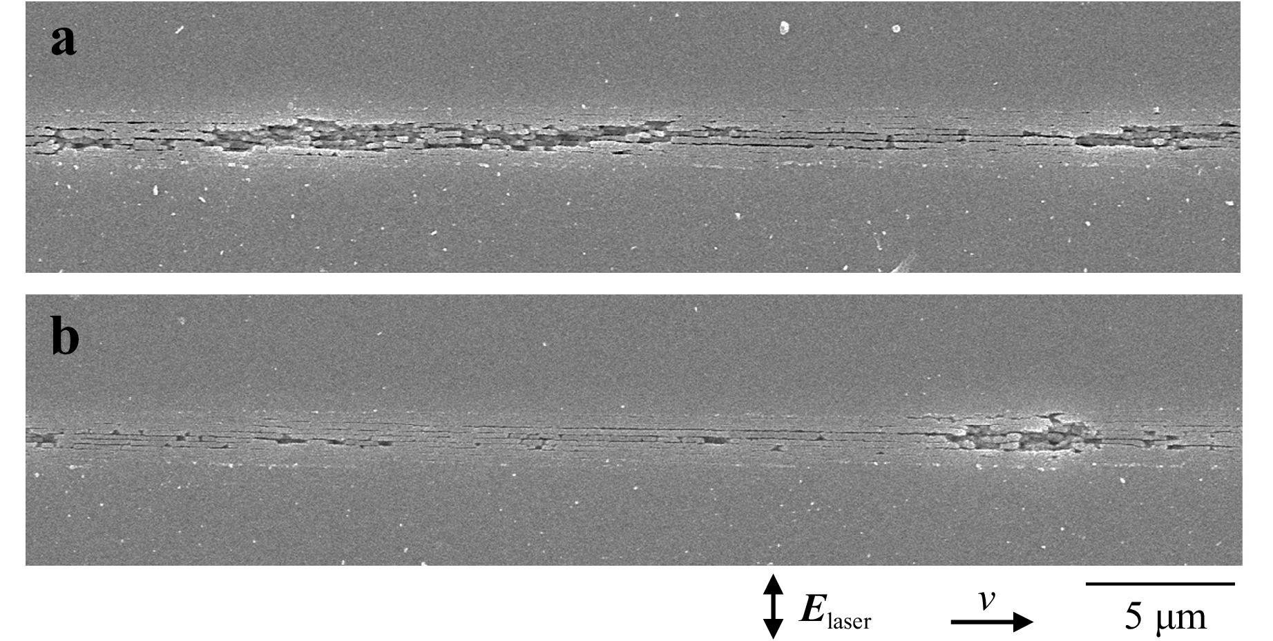
Fig. 5 SEM images of glass surfaces irradiated with fs laser pulses a without and b with feedback control of laser power. Elaser and v denote the polarisation direction for the fs laser pulses and scanning direction, respectively.
-
In this section, we discuss the origin of the decrease in the reflectance and increase in the transmittance of a glass surface with nanostructures. When a medium contains structures considerably smaller than the wavelength of light, as shown in the SEM images in Figs. 2-5, its refractive index can be effectively modelled as that of a flat film with a constant refractive index28–31. This approach, known as the effective medium approximation, is utilised for measuring film thickness in spectroscopic ellipsometry29 and explaining the anti-reflection effects seen on surfaces, such as moth eyes that have fine structures32–34. Using the Bruggeman model, which is commonly used in such analyses28,29,32, a material composed of a mixture of media with refractive indices n1 and n2 and their respective volume fractions f1 and f2 can be approximated as a uniform layer with an effective refractive index n expressed as follows:
$$ {f}_{1}\frac{{n}_{1}^{2}-{n}^{2}}{{n}_{1}^{2}+2{n}^{2}}+{f}_{2}\frac{{n}_{2}^{2}-{n}^{2}}{{n}_{2}^{2}+2{n}^{2}}=0 $$ (1) where f1 + f2 = 1. The cross-sectional SEM image of the nanostructure in Fig. 2a shows that eight grooves each with a width of approximately 20 nm and depth of approximately 1 μm were formed at intervals of approximately 200 nm on the glass surface. Therefore, this region measuring approximately 1.2 μm in width and 1 μm in depth consisted of air with f1 = 0.13 and synthetic silica glass with f2 = 0.87. Using the refractive indices of air and synthetic silica glass, n1 =1 and n2 =1.452 for a wavelength of 850 nm35, respectively, n =1.390 was estimated using Eq. (1) and is smaller than n2. Similarly, using n1 =1 and n2 = 1.456 for a wavelength of 660 nm35, n = 1.393 was obtained. By applying Fresnel’s equations, the reflectance R’ and transmittance T’ for a solid surface with a uniform layer at normal incidence were calculated to be 0.81 and 1.01, respectively. R’ was close to the experimental result R ≈ 0.54, as shown in Fig. 2a, whereas T’ was very different from T ≈ 1.48.
To understand the reason for this large increase in transmittance, we numerically calculated the propagation of light through the structured surface using the finite-difference time-domain (FDTD) method36,37. Fig. 6a-i show the phase distribution of the electric field of the illumination light at t = 36.9 and 22.7 fs after excitation (t = 0) and the amplitude distribution of the electric field at t = 45.0 fs, respectively. The light source, with a wavelength of 850 nm, was placed inside at a distance of 2.5 μm from the glass surface, and the polarisation direction of the light was horizontal. As shown in Fig. 6a-f, the wavefronts of the light transmitted through the three distinct surface geometries (nanostructure, nanostructure in dimples, and dimples only) were distorted into concave shapes. The boundary between the distorted and plane wavefronts is indicated by the black dashed lines in these figures. Because the numerical aperture (NA) was defined as the angle at which the ray spreads, the values can be estimated from the spread angle of the wavefront distortion38. From the slope of the dashed lines, these values were calculated to be 0.20, 0.25, and 0.39 for surfaces with nanostructures, nanostructures in dimples, and dimples only, respectively. In addition, when the polarisation direction of the light was vertical, the wavefront of the transmitted light exhibited a similar concave distortion, corresponding to NA values of 0.066, 0.24, and 0.40. These results indicate that the wavefront was distorted into a concave shape owing to the lower refractive index of the structured surface, and that the nanostructures were birefringent depending on the polarisation direction of the light.
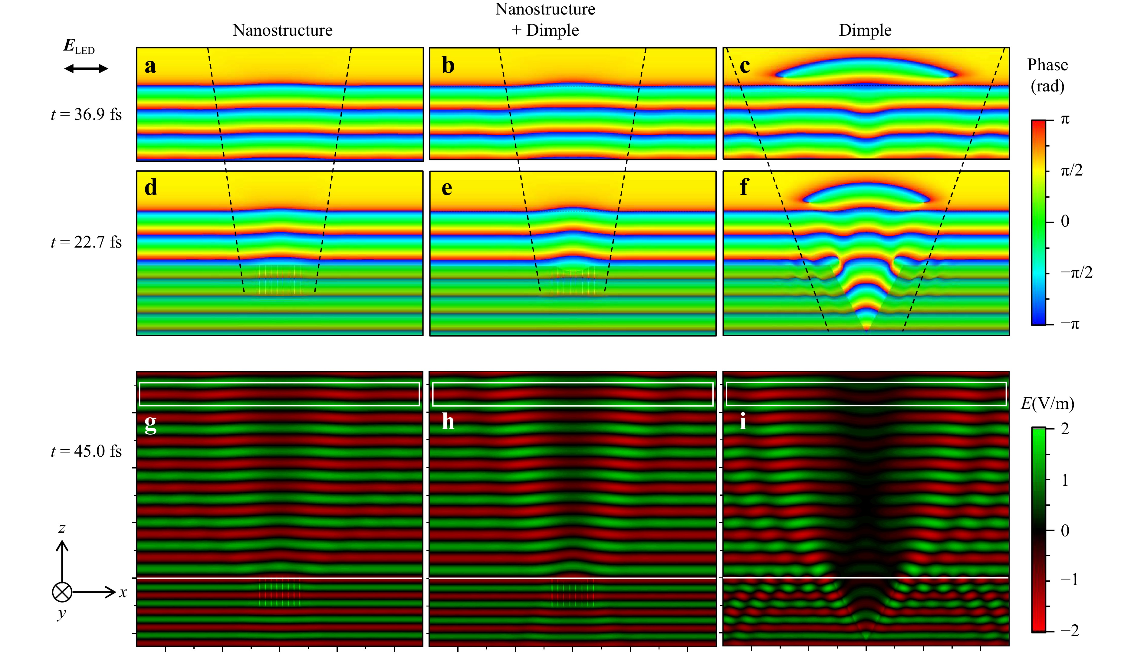
Fig. 6 Electric fields propagating near ablated glass surfaces. Phase distribution of electric fields propagating into a, d nanostructure, b, e nanostructure in dimple, and c, f dimple only. Amplitude distributions of electric fields propagating into g nanostructure, h nanostructure in dimple, and i dimple only. Dashed lines denote the edge of the distorted wavefront for easier tracking. ELED denotes the polarisation direction for the 850-nm light.
In this experiment, we used an infinity-corrected optical system to measure the R and T values of the glass surfaces. In this configuration, the light beam passing through the objective lens was collimated, and the imaging lens formed an image on the camera. By integrating the energy of the electric field within a 10-μm-wide region at a distance of 6–7 μm from the surface, as shown by the white rectangles in Fig. 6g, h, the energy of the transmitted light entering the pupil of the objective lens was equivalent to that of the flat surface in both polarisation directions by changing the polarization direction of the light source. This result indicates that the light transmitted from a nanostructured surface propagates to the camera without attenuation. Furthermore, the distorted wavefront of the transmitted light causes a large contrast enhancement at the centre of the image plane owing to interference39–43; thus, the transmittance of the nanostructured surface appears to increase. Conversely, in the case of a large dimple, the energy of the electric field, as shown by the white rectangles in Fig. 6i, decreased to 0.75, indicating a decrease in the transmittance owing to scattering. These results indicate that our in-process monitoring method for homogeneous nanostructure formation is sensitive to the glass-surface shape, owing to the structural birefringence induced by the nanostructures. This suggests that the proposed method can also be applied to transparent media.
In conclusion, we developed an optical system that can monitor nanostructure formation on glass surfaces induced by fs laser irradiation in real time. The system employs two pairs of cameras and LEDs with different wavelengths. In the ablation experiments, changes in the surface reflectance, transmittance, and morphology of the irradiated area were observed by varying the laser power, scanning speed, and polarisation direction of the fs laser pulses. When nanostructures are formed, these changes led to a decrease in reflectance and an increase in transmittance. Distinctive changes in these optical properties are effective for identifying the formation of homogeneous nanostructures. By implementing feedback control of the laser power based on these measurements, the proportion of defective regions in the laser-irradiated area was reduced by a factor of approximately 10. Therefore, this method is effective for the consistent formation of high-quality nanostructures on transparent materials.
-
The optical system used for this experiment is shown in Fig. 1. The setup included a target mounted on a three-axis automated stage. Linearly polarised laser pulses with a centre wavelength of 1030 nm, pulse width of 250 fs, and repetition rate of 20 kHz generated by an in-house chirped-pulse amplified ytterbium fibre-laser system were focused onto the target surface using an objective lens (OL) with NA = 0.4. The diameter of the focused spot was approximately 5 μm based on the e-2 intensity. An acousto-optic modulator (AOM) adjusted the laser power P within the range of 6.0–15 mW. A function generator (33522B, Keysight Technologies, USA) provided a DC voltage output of VFG = 7.0–8.0 V, as determined by the computer, and a radio-frequency (RF) circuit output an 80-MHz RF signal with a voltage amplitude proportional to VFG. This RF signal controlled the AOM to modulate P. In the ablation experiments, the target was moved horizontally at a scanning speed v of 1–1000 μm/s. During fs laser irradiation, compressed air was blown onto the target surface to prevent debris from adhering to the surface.
To measure the reflectance R and transmittance T of the target surface in real time during fs laser irradiation, optical microscopy images of the target surfaces were acquired using coaxial epi-illumination and transillumination. Two LEDs with wavelengths of 660 and 850 nm were used as sources for coaxial epi-illumination and transillumination, respectively, and R and T were measured simultaneously using two cameras. We used two wavelengths to prevent the illumination light from entering the two different cameras because the nanostructure-covered surface may diffract light. An LED light with a wavelength of 660 nm (LED1) was coaxially incident on the target surface and in the same direction as the fs laser with a half mirror. The illumination light reflected by the target passed through several optical components, including a dichroic mirror (DM), half mirror (HM), polariser (POL), and plano-convex lens with a focal length of f = 2000 mm (L). Subsequently, the reflected light was detected using a complementary metal-oxide semiconductor (CMOS) camera (C1). The polarisation direction of the detected light was determined using the POL. Conversely, an LED light with a wavelength of 850 nm (LED2) was coaxially incident in the direction opposite to that of the fs laser pulses. The light transmitted through the target was detected using another CMOS camera (C2). Before reaching C1 and C2, a short-pass and long-pass filters were implemented to selectively filter out light of different wavelengths. Moreover, the fs pulse was filtered with two DMs and was not detected by C1 or C2.
-
A synthetic silica-glass plate (ES series, Tosoh MGS Corp., Japan) with a thickness of 1 mm was used as the target material.
-
After laser irradiation, reflectance, and the transmittance measurements, a gold film with a thickness of approximately 25 nm was deposited on the target surface. The surface morphology was observed using SEM (JSM-6510, JEOL Ltd., Japan). To observe the cross-sectional morphology, a synthetic silica-glass plate was split using a glass cutter. The cross section was then examined using a field-emission SEM (S-4800, Hitachi High-Tech Corp., Japan).
The target surfaces observed using SEM were visually identified as having either uniform or defective nanostructures in the processed area. The defect ratio was defined as the ratio of the defective area to the entire processed area.
-
As shown in Fig. 2, the laser power P influences the surface morphology of the glass as well as its reflectance R and transmittance T. The desired setpoints for R′ and T′ were set to the values of R and T measured during the formation of a homogeneous nanostructure, and P was PID controlled44,45 to maintain these values. The error value $ e\left(t\right) $ represents the difference between the desired setpoints (R′ and T′) and measured values (R(t) and T(t)), and was calculated as $ e\left(t\right)=-\left(\left|{R'}-R\left(t\right)\right|+\left|{T'}-T\left(t\right)\right|\right) $ for $ R\left(t\right) < R'$ and $ e\left(t\right)=\left(\left|{R'}-R\left(t\right)\right|+\left|{T'}-T\left(t\right)\right|\right) $ for $ R' < R\left(t\right) $. The voltage output from the function generator was adjusted using the following formula:
$$ \Delta {V}_{\mathrm{F}\mathrm{G}}\left(t\right)={K}_{\mathrm{p}}e\left(t\right)+{K}_{\mathrm{i}}\int e\left(t\right)\mathrm{d}t+{K}_{d}\frac{\mathrm{d}e\left(t\right)}{\mathrm{d}t} $$ (2) where Kp = 5 V, Ki = 1 V/s, and Kd = 10 Vs were set to approach $ e\left(t\right)=0 $ and stabilise the system manually by R and T during the fs-laser irradiation. We did not implement a specific design to avoid overcorrection.
The feedback rate of 100 ms in the system was the working time for the following processes: (i) C1 and C2 detected the reflectance and transmittance images, respectively, and outputted them to the computer; (ii) the computer calculated R and T at the centre of the fs-laser irradiated area from the acquired images; (iii) the computer calculated ΔVFG using R, T, and Eq. 2 and sent the voltage value to the function generator; and (iv) the function generator drove the AOM via the RF circuit controlling the laser power P. In our system, processes (i) and (ii) required 86 ms because we used 32-fps cameras. We expect that this time can be shortened to 4 ms using high-frame-rate cameras and decreasing the region of interest in the exposed areas. Currently, high-speed photodetectors can monitor heat accumulation on the target surface in laser processing with a 2-μs acquisition time46, and custom integrated circuits such as a field programmable gate array (FPGA) can control laser welding in-process with a 1-ms feedback delay time47. Using high-speed detectors and an FPGA in our system may enable a feedback rate on the order of microseconds.
-
The distributions of the electric-field amplitude and phase of the transmitted light propagating across the structured glass surface were numerically calculated using the FDTD method36,37 (Fujitsu, Poynting for Optics). The calculation area was set to 20 μm, 11 μm, and 20 nm in the horizontal, vertical, and depth directions, respectively. Absorption boundary conditions were applied in the horizontal and vertical directions, and periodic boundary conditions were applied in the depth direction. Within this region, a section of atmosphere (air) with a refractive index of 1 was established. Furthermore, a rectangular block of synthetic silica glass with a refractive index of 1.452 and dimensions of 20 μm, 3.5 μm, and 20 nm in the horizontal, vertical, and depth directions, respectively, was placed within this atmospheric section. Inside the synthetic silica glass, a light-source plane was placed at a distance of 2.5 μm from the boundary with the atmosphere to emit a linearly polarised continuous wave with a wavelength of 850 nm and an amplitude of 1 V/m, covering an area of 6 μm in the horizontal direction and 20 nm in the depth direction. The three distinct surface geometries formed by the fs laser pulses shown in Fig. 2 were modelled as follows. For the surface with homogeneous nanostructures (shown in Fig. 2a), eight rectangles filled with atmosphere, each 20 nm wide and 1.0 μm deep, were placed at 200-nm intervals on the synthetic silica-glass surface. Next, for the surface with nanostructures in dimples (shown in Fig. 2b), eight rectangles of atmosphere, each 20 nm wide and 1.0 μm deep, were placed at 200-nm intervals within a cylindrical form with a radius of curvature of 1.0 μm and depth of 200 nm. Lastly, a triangular column with a width and depth of 2.5 μm represented the surface with dimples (shown in Fig. 2c).
-
The authors thank Prof. Dr. H. Minoda for his advice regarding the interference of the transmitted light. This study was supported by the New Energy and Industrial Technology Development Organization (NEDO), Japan.
Stable fabrication of femtosecond-laser-induced periodic nanostructures on glass using real-time monitoring and active feedback control
- Light: Advanced Manufacturing , Article number: (2025)
- Received: 03 September 2024
- Revised: 14 October 2024
- Accepted: 14 October 2024 Published online: 18 March 2025
doi: https://doi.org/10.37188/lam.2025.003
Abstract: Femtosecond laser pulses can be employed to directly form periodic nanostructures on solid surfaces, including hard materials such as diamond and sapphire, via ablation. Thus, this technique is promising for industrial nanofabrication applications. However, the stable formation of uniform nanostructures is challenging because of their high sensitivity to changes in processing conditions, such as the surface roughness of materials and laser power. Herein, we report a real-time monitoring and control approach for fabricating high-quality nanostructures on glass surfaces. We measured the reflectance and transmittance of a laser-irradiated surface simultaneously and determined their specific values corresponding to the formation of a uniform nanostructure with a period of 200 nm and depth of 1 μm. By utilising these values as feedback signals in a proportional-integral-derivative control system, we adjusted the laser power during irradiation to form a uniform nanostructure. This approach led to a significant reduction in the defect ratio of the nanostructure (~2.4%), which represents a 10-fold reduction compared with uncontrolled processing. Our results demonstrate the potential for the stable and direct fabrication of high-quality nanostructures on solids and offer a valuable method for the quality assurance of nanostructures for various applications.
Research Summary
Data-driven laser nanofabrication: real-time optical monitoring enables stable nanostructuring
Structures below the wavelength of light are expected to have various kinds of applications in optical devices because of their ability to control optical properties. Removal or bonding structure changes by ultrashort laser pulses can easily fabricate nanostructures on or inside solid surfaces. A collaborated group led by Dr. Godai Miyaji from TUAT, Japan and Dr. Aiko Narazaki from AIST, Japan has developed a technique for real-time optical monitoring of nanostructure formation by ultra-short laser pulses and demonstrated that high-quality nanostructures can be stably fabricated by actively controlling a laser parameter.
Rights and permissions
Open Access This article is licensed under a Creative Commons Attribution 4.0 International License, which permits use, sharing, adaptation, distribution and reproduction in any medium or format, as long as you give appropriate credit to the original author(s) and the source, provide a link to the Creative Commons license, and indicate if changes were made. The images or other third party material in this article are included in the article′s Creative Commons license, unless indicated otherwise in a credit line to the material. If material is not included in the article′s Creative Commons license and your intended use is not permitted by statutory regulation or exceeds the permitted use, you will need to obtain permission directly from the copyright holder. To view a copy of this license, visit http://creativecommons.org/licenses/by/4.0/.

 DownLoad: