


-
Nano-kirigami/origami has emerged as a significant research field due to its unique ability to create versatile three-dimensional (3D) nanostructures from two-dimensional (2D) planar patterns through flexible shape transformation1–8. This technology has found applications in light field manipulations1,9–11, holographic display12, thermal management13, and optoelectronic devices14. Various actuation methods of nano-kirigami/origami have been developed15,16, including capillary forces17–19, residual stress20,21, mechanical stress22–24, and focused-ion-beam (FIB) irradiation-induced stress1,25–28, depending on different environments and materials. In particular, the FIB irradiation-induced deformable nano-kirigami method, leveraging advanced semiconductor technology, offers a sophisticated approach to achieving miniaturized, direct, and in situ structural deformations1. A notable advantage of FIB-based nano-kirigami lies in its sensitivity to parameters such as accelerating voltage, dose, and irradiation pattern of the ion beam, alongside its dependence on the topological types of the 2D structures. From a topological classification perspective, nano-kirigami structures can be categorized into two groups: open-loop (tree-type) and close-loop28–30. Open-loop structures7, 25, 31-35 exhibit predictable deformations with notable optical properties, including multiple Fano resonance9,36, spin-selective transmission37, toroidal resonance34 and giant chirality31,32,38. However, their deformation is typically limited to direct bending and folding of individual structural components. In contrast, close-loop structures, featuring interrelated and nested components, enable in situ folding, buckling, rotation, and distortion, facilitating the creation of diverse kirigami structures1,10,39. Consequently, nanostructures based on close-loop designs have demonstrated competitive optical performances and have been applied in active phase control12,40, polarization10, optical chirality11,41,42, and nonlinear radiation43. Despite enriching nanostructure morphology, close-loop designs are constrained in deformation height by central connections. Therefore, a nano-kirigami strategy capable of achieving both significant deformations and versatile shapes is highly desirable to meet the diverse functionality and performance requirements of modern optical systems.
Here, we propose an exceptional kissing-loop nano-kirigami scheme that can directly transform nanostructures from 2D open-loop to 3D kissing-loop morphologies, which induces excellent modulation effects on the polarization and phase of the incident light. This precise bending and kissing method, which is based on FIB irradiation, is convenient in terms of spatial controllability compared to previous quasi-2D and 3D nano-kirigami/origami techniques, thus creating a novel structural topology for nano-kirigami/origami. Notably, kissing-loop nano-kirigami structures exhibit asymmetric transmission in the near-infrared wavelength region, which can be further adjusted by transforming their structural morphology. More importantly, the Pancharatnam-Berry geometric phase was experimentally realized for the first time in nano-kirigami structures, and cross-polarized reflection beams were anomalously reflected in broadband under the illumination of circularly polarized incident light. This FIB-defined kissing-loop nano-kirigami scheme fulfills the multiple desires of small size, high deformation, and exquisite 3D morphology and shows great potential for optical reconfiguration, optical communications, nanophotonic devices, etc.
-
A schematic of the kissing-loop nano-kirigami is shown in Fig. 1. The open-loop system in the first row of Fig. 1a can only achieve localized bending or folding, owing to the independent motion of each neighboring component. In contrast, the close-loop system in the middle row of Fig. 1a has interrelated structural components and can be used to construct continuously twisted 3D structures. However, owing to the central connections between different parts, the deformation height was limited. To overcome the limitations of the above two structures, we designed a kissing-loop nano-kirigami that is an open-loop in the 2D state and a kissing-loop in the 3D state when the two separated components are deformed and touch each other. In such cases, the structure has the advantages of a large deformation height and strong structural distortion. The bottom of Fig. 1a shows the structural parameters of kissing-loop nano-kirigami, where the period is $ {p}_{1}=1.7 $ μm in x and y direction. The widths of cantilevers and frame are $ {w}_{1}=0.21 $ μm and $ {w}_{2}=0.2 $ μm, respectively, and the thickness of gold film is $ d=60\;\mathrm{n}\mathrm{m} $. By reasonably adjusting these parameters, precise docking of the two cantilevers was achieved in the z-direction (see more details about the structural designs in Figure S1a).

Fig. 1 Scheme for kissing-loop nano-kirigami. a Deformation diagrams of open-loop, close-loop, and kissing-loop structures. Structural parameters of a unit cell of the kissing-loop structure, where $ {p}_{1} $, $ {w}_{1} $, and $ {w}_{2} $ are 1.7, 0.21, and 0.2 μm, respectively. b Deformation height ($ \Delta h $) versus the applied stress in the film for open-loop (blue line), close-loop (black line), and kissing-loop (red line) structures. For the kissing-loop scheme, the tips of the two cantilevers just touch at stress σ = 1.65 GPa and $ \Delta h=760 $ nm. c Illustration of the helical array and flower-window structure designed based on kissing-loop nano-kirigami.
For quantitative analysis, in Fig. 1b we compare the deformation height ($ \Delta h $) of the above three geometric configurations under the same stress using the bilayer stress model (see more details in the Section I of Supporting Information)1. The blue line and black line verify that an open-loop structure can be deformed with height several times larger than that of a close-loop structure under the same stress. The kissing-loop nano-kirigami with a well-designed initial open-loop 2D structure not only has a large deformation height but also transforms into a kissing configuration during upward bending (red line). Specifically, the deformation height of the kissing-loop nano-kirigami increases with the increase of the stress while the tips of two cantilevers get close until kissing at a stress of σ =1.65 GPa. The two cantilevers were further separated under continuous ion-beam irradiation (Figure S1c). In these cases, the structural morphology can be precisely controlled by adjusting the irradiation dose. Based on this kissing-loop nano-kirigami scheme, extensive geometries with diverse feature sizes can be realized for many different classes of materials. For example, 2D open-loop units arranged periodically in the x or y direction can be assembled into a uniform lying-down 3D helical coil under low-dose global FIB irradiation, as illustrated in the upper part of Fig. 1c. Similarly, cantilevers located inside the sector frame can constitute a flower-window structure under low-dose global FIB irradiation, as shown at the bottom of Fig. 1c. It is expected that a metalens can be designed by rotating the optical axis of the kissing-loop nano-kirigami structural unit and carefully arranging it radially. Therefore, kissing-loop nano-kirigami goes beyond the traditional topological classification, breaking spatial symmetry with an exotic deformation mechanism, and has high scalability.
-
The basic principle is that when the FIB irradiates the gold film, the defects generated in the film and the implanted gallium ions induce different types of stresses that deform the structures and achieve a new mechanical equilibrium state (see more details in Section I of the Supporting Information). For experimental demonstration, kissing-loop nano-kirigami structures were fabricated on a SiO2 substrate deposited with a 60-nm-thick Au film. A gold film on a SiO2 substrate is flatter, smoother, and easier to handle than a suspended gold film that requires sophisticated skills and time-consuming preparation, which is advantageous for large-scale nanofabrication. Specifically, the fabrication process consists of three steps in which 2D nanopatterns are deformed into 3D structures: lithography of the deliberately designed 2D open-loop patterns with a high-dose FIB, suspension by wet etching, and global irradiation with a low-dose FIB, as illustrated in Fig. 2a. As shown in Fig. 2b−d, the helical array and flower-window structure shown in Fig. 1c are well reproduced. It should be mentioned that the large-area kissing-loop nano-kirigami array with a narrow square supporting frame sometimes collapses owing to the capillary force during the wet-etching process. To overcome this issue, the structural design is optimized by replacing the square frame with a circular frame and reduce the period to $ {p}_{2}=1 $μm (see specific parameters in Figure S1b). The key point of this optimization is that a wider circular frame can retain the SiO2 pillars during the etching process, thereby providing effective support for the structure. The successful wet-etching results are illustrated in column (i) of Fig. 2b−d, based on which the two cantilevers were synchronously bent upward to achieve perfect kissing by low-dose FIB scanning, as shown in columns (ii)–(iii). Because the deformation of the kissing-loop structures is attributed to the irreversible and stable residual stress resulting from FIB irradiation, the kissing-loop nano-kirigami structures were very stable under no intense disturbance. In addition, to achieve definite touch after deformation, a high consistency in the deformation of the cantilevers is required, and the arm length of the cantilevers is designed to be slightly larger than the ideal case so that there is an increased opportunity for touching in the upward deformation pathway (see more details in Figure S2), where the error tolerance is determined by half of the arm width. To ensure good contacts and high uniformity across the entire array, the FIB irradiation employed the standard scan direction of “Dynamic All Directions” and utilized low-dose multiple scanning to attain a success rate exceeding 90%. These exquisite kissing-loop structures are difficult to realize using traditional 3D nanofabrication methods, which significantly broadens the design principles of nanophotonic devices and micro-/nanoelectromechanical systems (MEMS/NEMS). Moreover, the kissing-loop nano-kirigami method is not limited to gold films and is also applicable to silver, aluminum, semiconductors, phase-change materials, and dielectric materials. Several potential scalable fabrication and actuation methods exist for different materials. For instance, electron beam lithography (EBL) beyond FIB can be used to fabricate 2D nanopatterns in large areas14, whereas capillary force and residual stress can also bend or fold microstructures to achieve closed folding19,27.

Fig. 2 Fabrication of kissing-loop nano-kirigami structures. a Schematic diagram of the nanofabrication process of kissing-loop nano-kirigami on Au/SiO2 substrate. b−d SEM images of various kissing-loop structures. (i) SEM images of 2D open-loop precursors after FIB milling and wet-etching, as well as side-view (ii) and top-view (iii) of 3D kissing-loop nano-kirigami structures after global FIB irradiation from the top. Scale bars: 1 µm.
-
The kissing-loop nano-kirigami array, with a period as small as 1 μm, provides a promising platform for 3D functional nanophotonic and optoelectronic devices. Here, the asymmetric transmission of kissing-loop nano-kirigami was first explored, as shown in Fig. 3a. The transmission coefficients for x- and y-polarized incidences along the forward (+z direction) can be determined using the Jones matrix44–46

Fig. 3 Asymmetric transmission of kissing-loop nano-kirigami. a Schematic of asymmetric transmission of kissing-loop nano-kirigami structures at x-polarized incidence. b,c Simulated cross-polarized transmission spectra of 2D open-loop and 3D kissing-loop structures under backward and forward incidence, respectively. d SEM images of the fabricated arrays (20 × 20 μm2) of 2D open-loop and 3D kissing-loop nano-kirigami structures. Scale bars: 1 µm. e,f Experimentally measured cross-polarized transmission spectra of 2D open-loop and 3D kissing-loop structures under backward and forward incidence, respectively.
$$ {T}_{lin}^{f}=\left(\begin{array}{cc}{t}_{xx}& {t}_{xy}\\ {t}_{yx}& {t}_{yy}\end{array}\right) $$ (1) where the indices f indicate propagation in the forward direction and the subscript ij (i = x,y; j = x,y) indicates that the j-polarized incident wave is converted into i-polarized transmission. According to the reciprocity theorem, the Jones matrix for backward incidence (-z direction) can be derived as
$$ {T}_{lin}^{b}=\left(\begin{array}{cc}{t}_{xx}& -{t}_{yx}\\ {-t}_{xy}& {t}_{yy}\end{array}\right) $$ (2) where b indicates propagation in the backward direction. The asymmetric transmission parameters $ \Delta $ for the x- and y-polarized waves are defined as
$$ {\Delta }_{lin}^{\left(x\right)}={|{t}_{yx}|}^{2}-{|{t}_{xy}|}^{2}={-\Delta }_{lin}^{\left(y\right)} $$ (3) As the deformation of 2D-to-3D, the mirror symmetry of the 2D structure within its own plane is disrupted and the 3D kissing-loop nano-kirigami structure possesses two-fold rotational symmetries (C2) only with respect to the z-axis, which satisfies the condition for asymmetric transmission of linear polarization, $ |{t}_{xy}|\ne |{t}_{yx}| $. The simulated transmission spectra (Figure S3a, b) show that the cross-polarized transmission spectra for x- and y-polarized incidence are opposite (red and green lines), achieving the asymmetric transmission parameters $ |{\Delta }_{lin}^{\left(x\right)}|=|{\Delta }_{lin}^{\left(y\right)}|=0.26 $ (Figure S3c). In addition, Figure S3a, b demonstrate that the co-polarized transmission of linearly polarized light remains consistent under forward and backward incidence, implying that asymmetric cross-polarized transmission also results in an asymmetric total transmission. Asymmetric transmission also occurs when circularly polarized light is incident; however, owing to its weak intensity, it will not be further discussed here. Next, we use x-polarized incident wave along the forward and backward directions as an example to further explain these phenomena (the incident y-polarized wave has similar conclusions).
Fig. 3b, c plot the simulated transmission spectra of 2D open-loop structure array and 3D kissing-loop structure array with x-polarized incidence along backward and forward directions, respectively. For the 2D open-loop structure, the transmission spectra of backward incidence and forward incidence are almost identical, and the resonance peak of cross-polarized light appears at 1.37 μm with $ {T}_{yx} $ = 0.1, as shown by the black curves in Fig. 3b, c. In contrast, the $ {T}_{yx} $ of 3D kissing-loop structure is almost zero under the backward incidence, indicating there is no obvious polarization conversion. Interestingly, a transmission peak of 3D kissing-loop structure appears at 1.63 μm under the forward incidence, with a remarkable peak of $ {T}_{yx}= $ 0.28, as noted by the red curves in Fig. 3b, c. This obvious difference in transmission between forward/backward excitation indicates an effective asymmetric transmission effect of kissing-loop nano-kirigami structures. Meanwhile, Fig. 3c shows that both the peak and intensity of the cross-polarized transmission spectra can be adjusted by transforming 2D open-loop structures to 3D kissing-loop structures. In order to reveal the physical mechanism of asymmetric transmission, the reflection/transmission spectra (Figure S4a, b) and the electric field intensity distributions at λ = 1.63 μm (Figure S4c, d) of 3D kissing-loop structures are simulated for x-polarized waves incident along the backward and forward directions, respectively. By comparing the electric field intensity distributions under backward and forward incidence, it can be found that this asymmetric transmission is mainly derived from the structural spatial distortion caused by the unidirectional deformation of kissing-loop nano-kirigami structures.
To verify the above simulations and analysis, the experimental transmission spectra of 2D open-loop structures and 3D kissing-loop structures in Fig. 3d (with characterization area of 15 × 15 μm2) are measured with a home-built microscopy system (Figure S5 of Supporting Information). The experimental results in Fig. 3e, f clearly reveal the asymmetric transmission of the cross-polarized light for the 3D kissing-loop structures, with a forward incidence of $ {T}_{yx} $ = 0.2 and a backward incidence of $ {T}_{yx}=0.02 $ at the same wavelength. A red shift in the cross-polarized transmission peak was observed when the structures were deformed from 2D to 3D geometries. Thus, for kissing-loop nano-kirigami structures, the experimental results show good consistency with the simulated results, while the mismatch of resonance wavelength and intensity between the simulation and experiment is mainly attributed to the background noise in the measurement and the imperfect structural morphology induced by high-energy ion dose implantation33. The imperfect structural morphology is mainly reflected in the modifications to the width of the cantilevers and the thickness of the gold film caused by ion beam irradiation, which weakens and red-shifts the resonance peak (see more details in Figure S6a, b).
-
Kissing-loop nano-kirigami structures also allow for the wavefront shaping of circularly polarized light (CPL) by utilizing the Pancharatnam-Berry (PB) phase. The two principal axes of the structure are u and v (Figure S7). In general, the reflection properties of metasurfaces are characterized by a Jones matrix47
$$ R\left(0\right)=\left(\begin{array}{cc}{r}_{uu}& {r}_{uv}\\ {r}_{vu}& {r}_{vv}\end{array}\right) $$ (4) Considering the case that the structural unit is rotated by an angle $ \phi $ with respect to the z axis, the new Jones matrix is
$$\begin{split} R\left(\phi \right)=\;&M\left(-\phi \right)R\left(0\right)M\left(\phi \right)\\=\;&\left(\begin{array}{cc}cos\phi & -sin\phi \\ sin\phi & cos\phi \end{array}\right)\left(\begin{array}{cc}{r}_{uu}& {r}_{uv}\\ {r}_{vu}& {r}_{vv}\end{array}\right)\\&\left(\begin{array}{cc}cos\phi & sin\phi \\ -sin\phi & cos\phi \end{array}\right) \end{split}$$ (5) Under the normal incidence, LCP light and RCP light can be expressed as
$$ {E}_{in}^{L}=\frac{1}{\sqrt{2}}\left(\begin{array}{c}1\\ i\end{array}\right)\;\; {\rm{and}}\;\; {E}_{in}^{R}=\frac{1}{\sqrt{2}}\left(\begin{array}{c}1\\ -i\end{array}\right) , \;{\rm{respectively}} $$ (6) Hence, the reflected field can be written as
$$ \begin{split}{E}_{out}^{L}=\;&R\left(\phi \right){E}_{in}^{L}=\frac{1}{2\sqrt{2}}\left[{r}_{uu}+{r}_{vv}+i\left({r}_{uv}-{r}_{vu}\right)\right]\left(\begin{array}{c}1\\ i\end{array}\right)\\& +\frac{1}{2\sqrt{2}}\left[{r}_{uu}-{r}_{vv}+i\left({r}_{uv}+{r}_{vu}\right)\right]{e}^{i2\phi }\left(\begin{array}{c}1\\ -i\end{array}\right) \end{split}$$ (7) $$ \begin{split}{E}_{out}^{R}=\;&R\left(\phi \right){E}_{in}^{R}=\frac{1}{2\sqrt{2}}\left[{r}_{uu}+{r}_{vv}-i\left({r}_{uv}-{r}_{vu}\right)\right]\left(\begin{array}{c}1\\ -i\end{array}\right)\\& +\frac{1}{2\sqrt{2}}\left[{r}_{uu}-{r}_{vv}-i\left({r}_{uv}+{r}_{vu}\right)\right]{e}^{-i2\phi }\left(\begin{array}{c}1\\ i\end{array}\right)\end{split} $$ (8) It can be seen that no matter what kind of CPL is incident, the outgoing field consists of both LCP and RCP lights, and the component spinning opposite to the incident wave will have a $ 2\phi $ geometric phase, which is the so-called PB geometric phase47–51.
To establish a phase distribution of the cross-polarization of the reflected beam for wavefront manipulation, we designed a metasurface with a PB geometric phase based on kissing-loop nano-kirigami, as illustrated in Fig. 4a. Firstly, the eight 2D open-loop units with an increment in rotation angle of $ \Delta \phi $= 22.5° between adjacent units are designed. Subsequently, 3D kissing-loop units were obtained using FIB global irradiation. First, we simulated the reflection spectra of kissing-loop nano-kirigami structures under LCP and RCP incidences. Fig. 4b shows that the cross-polarized reflection was significantly higher than the co-polarized reflection at the resonance wavelength for both LCP and RCP incidence. In particular, the cross-polarized reflection of kissing-loop nano-kirigami reaches up to ~60% at 1.73 μm under the normally incident RCP. Figure S8a, b show the reflection spectra of the kissing-loop structures with different rotation angles under LCP and RCP normal incidence, respectively. The reflection of eight kissing-loop units at resonance wavelength of 1.73 μm is extracted in Fig. 4c. It can be seen that the cross-polarized reflection is robust with respect to the rotation angle of 3D kissing-loop structure. The calculated reflection phase profiles of the kissing-loop nano-kirigami manifest the spin-dependent linear phase gradients and cover the entire range from 0 to 2π, as plotted in Fig. 4d. As a result, the kissing-loop metasurface can deflect LCP and RCP light in opposite directions, as illustrated in Fig. 5a. Fig. 5c plots the simulated phase distributions of the diffracted light at 1.3 μm, 1.73 μm and 2.5 μm, respectively, under LCP and RCP incidence, demonstrating the presence of broadband anomalous reflection in near-infrared range. The reflected lights are deflected to −x and +x directions under LCP and RCP incidence, respectively. The anomalous reflection angle is determined by the generalized Snell’s law49,52 which considers the contribution of the phase gradient:

Fig. 4 PB geometric phase of kissing-loop nano-kirigami. a Distribution of 2D open-loop and 3D kissing-loop nano-kirigami units with eight different rotation angles $ \phi $. b Simulated reflection spectra of kissing-loop nano-kirigami with $ \phi =0 $° under LCP and RCP incidence, respectively. $ {R}_{RR} $ and $ {R}_{LR} $ represent the co-polarized and cross-polarized reflection efficiency under RCP light incidence, respectively. $ {R}_{LL} $ and $ {R}_{RL} $ are the co-polarized and cross-polarized reflection efficiency under LCP light incidence, respectively. c,d Simulated cross-polarized reflection (c) and corresponding phase (d) of eight kissing-loop nano-kirigami units at 1.73 μm under LCP and RCP incidence, respectively.
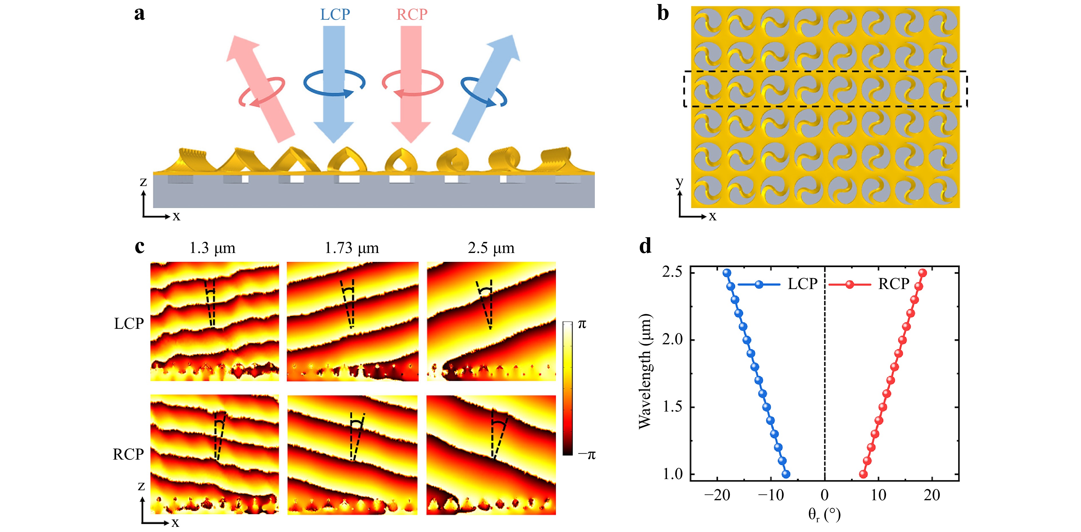
Fig. 5 Anomalous reflection scheme. a Schematic of anomalous reflection of kissing-loop metasurface by introducing geometric phase, where anomalous reflections are produced under LCP and RCP incidence, respectively. b Top view of a super unit (denoted by dashed rectangle) of the metasurface. c Simulated phase distributions of reflected cross-polarized light for kissing-loop metasurface at λ = 1.3 μm, 1.73 μm, and 2.5 μm, respectively, when LCP and RCP are normally incident. The anomalous reflection angle $ {\theta }_{r} $ increases with longer wavelengths. d Calculated $ {\theta }_{r} $ under LCP and RCP incidence with different wavelengths.
$$ sin{\theta }_{r}-sin{\theta }_{i}=\frac{{\lambda }_{0}}{2\pi {n}_{i}}\frac{d\Phi }{dx} $$ (9) where $ {\theta }_{i} $ and $ {\theta }_{r} $ are the angles of the incident and reflected waves; $ {n}_{i} $ is the refractive indices of medium; $ {\lambda }_{0} $ is the working wavelength; and phase shift $ \Phi =2\sigma \phi $, where $ \phi $ is the orientation angle of the nanostructure and $ \sigma =\pm 1 $ is dependent on circular polarization handedness. By easily deriving, the reflection angle $ {\theta }_{r} $ in the air can be expressed as40,52–54
$$ {\theta }_{r}={sin}^{-1}\left(sin{\theta }_{i}\pm \frac{{\lambda }_{0}}{S}\right) $$ (10) where S = 8 μm is the length of a supercell unit in x direction (dashed boxes in Fig. 5b). Thus, the calculated deflection angles under RCP incidence are 9.4°, 12.5°, 18.2° at 1.3 μm, 1.73 μm, 2.5 μm, which are reversed under LCP incidence. According to Equation (10), the anomalous reflection angle θr can be increased by increasing wavelength λ or decreasing the period of the supercell unit S.
To characterize the broadband anomalous reflection experimentally, kissing-loop nano-kirigami samples were fabricated, as shown in Fig. 6a, b. The whole sample area in Fig. 6b is $ 40\;\times\; 40\;{\text{μ}\mathrm{m}}^{2} $ and the area of sample used for optical characterization is $ 25\;\times\; 25\;{\text{μ}\mathrm{m}}^{2} $, corresponding to signal collection from ~625 sample units. This large number of sample units guaranteed measurement accuracy. The angular resolution spectra were measured using a commercial Angle-Resolved Micro-Spectrometer ARMS (see the measurement setup in Figure S9 of the Supporting Information). As shown in Fig. 6c, the far-field intensity distribution exhibits two peaks under LCP incidence at λ = 1.6 μm, with one normal reflection at 0°, and an anomalous reflection at −12.3° (basically matched with the calculated $ {\theta }_{r} $ = −11.5° at λ = 1.6 μm). In contrast, under RCP, the anomalous reflection mode in Fig. 6d appears at +11.5°. To further demonstrate the broadband anomalous reflection of this kissing-loop metasurface, 2D color maps are plotted in Fig. 6e, f based on the experimental results, clearly showing the far-field reflected intensity as a function of the reflection angle $ {\theta }_{r} $ and the wavelength λ. The central bright bands (zeroth order) are attributed to the unmodulated spin component of the reflected beam, whereas the bright bands denoting the +1st or −1st orders stem from anomalous reflections under RCP and LCP light incidence, respectively. Both show good agreement with the simulation results shown in Fig. 5d. Moreover, Fig. 6e, f indicate the presence of significant broadband anomalous reflections in the wavelengths from 1.3 to 1.6 μm (the maximum wavelength is limited by the detectivity of the detector), with $ {\theta }_{r} $ increasing at longer wavelengths. This behavior agreed well with the calculated results shown in Fig. 5d, which were predicted using Equation (10). The standard deviation of the experimental results over different regions of the sample was within 10%, which was determined by both the fabrication and nanofabrication accuracies. Owing to the modifications to the width of the cantilevers and the thickness of the gold film in the fabrication process (see more details in Figure S6c, d), as well as the imperfection of the optical collection setup, the measured anomalous reflection light intensity was relatively weak compared to the zeroth-order reflection of the co-polarized light.

Fig. 6 Experimental measurements of anomalous reflection. a SEM image of kissing-loop nano-kirigami based on the PB-phase design. Scale bar: 1 μm. b SEM image of the fabricated kissing-loop metasurface (40 × 40 μm2). Scale bar: 5 μm. c, d Reflected light intensity distribution measured as a function of the reflection angles $ {\theta }_{r} $ for kissing-loop metasurface under LCP and RCP normal incidence, respectively, at λ = 1.6 μm. e, f Reflected light intensity as a function of the wavelength λ and the reflection angle $ {\theta }_{r} $, measured by an Angle-Resolved Micro-Spectrometer (ARMS).
-
In summary, we have introduced and demonstrated a novel strategy using kissing-loop nano-kirigami to construct 3D structures that differ significantly from traditional nano-kirigami designs employing open-loop and close-loop geometries. Through meticulous structural design and precise FIB processing, we achieved a period of 1 μm in the kissing-loop structures, introducing new topological possibilities compared to conventional 2D metasurface designs with grating-like structures55, rectangular units56, and elliptical units57. This study provides a fresh concept for designing and fabricating complex 3D micro/nanodevices. The significance lies in the topological transformation enabled by kissing-loop nano-kirigami, offering enhanced capabilities for amplitude, polarization, and phase manipulation, particularly in dynamic polarization and phase modulation applications. Significant asymmetric transmission was observed in the kissing-loop nano-kirigami array due to its unidirectional deformation, distinct from the superposition effects of multilayer micro-/nano-structures45,46. Furthermore, we achieved experimental realization of a PB-phase metasurface in nano-kirigami structures for the first time, demonstrating broadband anomalous reflection under RCP and LCP incidences. Our findings highlight the excellent performance of kissing-loop nano-kirigami in multifunctional optical field manipulation, promising applications in spatial light modulation, micro/nanoscale sensing, nanophotonics, optoelectronic devices, and beyond58.
-
Mechanical and optical simulations of kissing-loop nano-kirigami structures were conducted using the solid mechanics and wave optics modules of the finite element software COMSOL Multiphysics. Mechanical deformations of kissing-loop nano-kirigami structures were modeled using a bilayer stress distribution model1. With incident light propagating along the z-axis direction, optical transmission spectra and optical reflection spectra were simulated. Periodic boundary conditions were applied to the unit cells to create square lattices in the x-y plane.
-
A 5-nm-thick chromium layer and a 60-nm-thick gold layer deposited on a 500-μm-thick SiO2 substrate using a magnetron sputtering machine (Lab 18, Lesker) were utilized to fabricate the kissing-loop nano-kirigami structures. Firstly, the gold film was milled by FIB (FEI Helios G4 UC, Thermo Fisher Scientific) with a high-dose ion beam ($ > 600\;\mathrm{p}\mathrm{C}{\text{μ}\mathrm{m}}^{-2} $). Next, the sample was immersed in dilute hydrofluoric acid (20%, HF: H2O= 1:4) to etch away the underlying SiO2, resulting in locally suspended gold nanopatterns on the surface. Finally, the suspended 2D patterned areas were deformed by global FIB irradiation with a low-dose ion beam, forming 3D kissing-loop nano-kirigami arrays. During fabrication, the Ga+ ion beam was set to an acceleration voltage of 30 kV and a current of 40 pA. To ensure uniformity and good contact across the entire array, the scan direction was set to "Dynamic All Directions" mode, employing a low-dose multiple scanning method. For instance, the 40 × 40 μm2 array shown in Fig. 6b required approximately 20 scans at a dose of $ 6.3\times {10}^{-14}\;\mathrm{p}\mathrm{C}{\text{μ}\mathrm{m}}^{-2} $.
-
Transmission spectra were measured using a home-built optical system (see Figure S5 in the Supporting Information). Supercontinuum light sources (SC-Pro, YSL) with a repetition rate of 5 MHz were collimated before passing through a linear polarizer (650–2000 nm, Thorlabs) to obtain x-polarized light. This light was then transmitted through a fiber. An objective lens (×10, numerical aperture NA 0.3, Olympus) focused the incident waves onto the sample. Another near-infrared (NIR) objective lens (×10, NA 0.3, Olympus) collected the transmitted signals, which were subsequently delivered to a spectrometer (1000–2200 nm, NIRQuest, Ocean Optics). A linear polarizer positioned behind the collection objective lens facilitated the collection of cross-polarized transmission. An NIR CCD camera (MER-500-14U3C-L, Daheng Imaging) was installed in the switchable optical path for imaging. In the anomalous reflection experiments, the far-field reflected intensity was measured using a commercial Angle-Resolved Micro-Spectrometer (ARMS, Ideaoptics). A high-power halogen light source (HL-100, Ideaoptics) was collimated before passing through a linear polarizer (300–4000 nm, Thorlabs) and a quarter-wave plate (1100–2000 nm, Thorlabs) to achieve circularly polarized incidence. A near-infrared (NIR) objective lens (×100, NA 0.85, Olympus) focused the incident wave onto the sample and collected the reflected signals, which were then delivered to a SWIR camera (900 to 1700 nm, Nirvana-640, Princeton Instruments). A CCD camera (Dhyana 400DC, Tucsen) was positioned along the optical path for imaging.
-
This study was supported by the National Natural Science Foundation of China (Grant No. T2325005, 62375016), and Science and Technology Project of Guangdong (2020B010190001). The authors thank the Analysis and Testing Center from BIT for assistance with facility support.
Kissing-loop nano-kirigami structures with asymmetric transmission and anomalous reflection
- Light: Advanced Manufacturing , Article number: (2024)
- Received: 11 March 2024
- Revised: 20 July 2024
- Accepted: 26 July 2024 Published online: 22 October 2024
doi: https://doi.org/10.37188/lam.2024.042
Abstract: Nano-kirigami technology enables the flexible transformation of two-dimensional (2D) micro/nanoscale structures into three-dimensional (3D) structures with either open-loop or close-loop topological morphologies, and has aroused significant interest in the fields of nanophotonics and optoelectronics. Here, we propose an innovative kissing-loop nano-kirigami strategy, wherein 2D open-loop structures can transform into 3D kissing-loop structures while retaining advantages such as large deformation heights and multiple optical modulations. Benefited from the unidirectional deformation of the structures, the kissing-loop nano-kirigami exhibits significant asymmetric transmission under x-polarized light incidence. Importantly, the Pancharatnam-Berry geometric phase is experimentally realized in nano-kirigami structures for the first time, resulting in broadband anomalous reflection in the near-infrared wavelength region. The kissing-loop nano-kirigami strategy can expand the existing platform of micro/nanoscale fabrication and provide an effective method for developing optical sensing, spatial light modulations, and optoelectronic devices.
Research Summary
Kissing-loop nano-kirigami: Versatile 3D kirigami with novel structural topology
Kissing-loop nano-kirigami with novel structural topology shows great applications in asymmetric transmission and anomalous reflection. Nano-kirigami enables versatile shape transformation from 2D precursors to 3D architectures with simplified fabrication complexity and unconventional structural geometries. Jiafang Li from China’s Beijing Institute of Technology now reports an innovative kissing-loop nano-kirigami scheme that can directly transform nanostructures from 2D open-loop to 3D kissing-loop morphologies. Benefited from the unidirectional deformation of the structures, the kissing-loop nano-kirigami exhibits significant asymmetric transmission under x-polarized light incidence. Importantly, the Pancharatnam-Berry geometric phase was experimentally realized in nano-kirigami structures for the first time, resulting in broadband anomalous reflection in the near-infrared wavelength region.
Rights and permissions
Open Access This article is licensed under a Creative Commons Attribution 4.0 International License, which permits use, sharing, adaptation, distribution and reproduction in any medium or format, as long as you give appropriate credit to the original author(s) and the source, provide a link to the Creative Commons license, and indicate if changes were made. The images or other third party material in this article are included in the article′s Creative Commons license, unless indicated otherwise in a credit line to the material. If material is not included in the article′s Creative Commons license and your intended use is not permitted by statutory regulation or exceeds the permitted use, you will need to obtain permission directly from the copyright holder. To view a copy of this license, visit http://creativecommons.org/licenses/by/4.0/.

 DownLoad: