


-
In the field of micro- and nanofabrication, multi-photon 3D laser nanoprinting has become a mature and widespread technology1-8. The major challenges in this field are to further boost print speed, increase spatial resolution, make available a larger variety of dissimilar materials, and to democratize the technology in the sense of drastically reducing size and cost of such instruments9-11. While a lot of recent research tackles the first points, we address the last point of the list in this paper – while upholding excellent spatial resolution at the optical-diffraction limit.
Two-photon or multi-photon absorption processes are commonly used in polymer 3D laser printing because they introduce a nonlinearity that suppresses unwanted accumulation of light-induced exposure in the tails of a diffraction-limited laser focus (“proximity effect”)1. Today, far more than thousand users worldwide employ corresponding commercial instrumentation for applications ranging from micro-optical components, micro-robots, scaffolds for cell culture, to mechanical metamaterials1. Often, the instrumentation is run in cleanrooms in multi-user facilities, as the cost of such instruments lies in the range of half a million to a million Euros or US Dollars. The instruments are table-top, but still have volumes of hundreds of liters. Cost and volume are to a large degree connected with the necessity of pico- or femtosecond lasers for making two-photon absorption sufficiently efficient. These aspects make the technology hard to access for many small university groups.
Alternative approaches to obtaining such nonlinearity include the possibility of exploiting chemical instead of optical nonlinearities11-13. One recently introduced effective optical nonlinearity is to use the sequential absorption of two photons instead of the simultaneous absorption of two photons. We have referred to such sequential processes as one-color two-step absorption10. Two-color two-step absorption has been discussed as well14, where the two subsequent one-photon absorption processes can differ in their transition energy. We note that two-step absorption is one mechanism out of a broader family of mechanisms that we have summarized as (1+1)-photon absorption15. Here, we start from one-color two-step absorption because its performance is presently superior to other (1+1) mechanisms (see Fig. 3 in Ref. 15). In particular, using 405 nm wavelength GaN continuous-wave semiconductor edge-emitting laser diodes at necessary laser powers below 1 mW, one-color two-step absorption has allowed for 3D laser nanoprinting with 100 nm lateral spatial resolution and print speeds of up to 4 mm/s10.
The novelty of the present paper lies in that we not only use a miniaturized laser but miniaturize the entire 3D laser nanoprinter such that the entire system fits into a shoe box. Our miniaturization of the scan unit is based on a miniature MEMS (micro-electro-mechanical-systems) mirror scanner that enables scanning in the xy-plane of the sample. We have designed much of the optics in our printer such that it becomes compatible with the only 1.6 mm diameter of the MEMS mirror. Approaches presented by other authors have aimed at miniaturization and cost-cutting of the optical setup by using an optical-pickup-unit used for reading and writing from optical storage disks such as Blu-rays16,17. Their xy- and z-scanning, however, is based on slow and bulky linear stages and the systems were used for stereolithography only. Other recent approaches have started from the microscope stand of a commercial inverted optical microscope, and used two-step absorption18. In contrast, our 3D laser nanoprinter, including its optical as well as its electronic components, fits into a shoe box. In what follows, we start by describing the design of our system. Next, we characterize its performance, including printing a number of standard test structures.
-
To miniaturize 3D laser nanoprinters, a detailed critical look at each component of state-of-the-art printers is necessary. We identify five major crucial elements – light source, power modulation, scan unit, microscope objective lens, and the control unit – combined with few further essential yet minor optical components such as lenses, mirrors, and beam splitters19. The overarching goal of this paper is to reduce both the number of components involved and their cost, while upholding the printing capability of the setup.
Fig. 1 depicts a scheme of the optical setup of our shoe-box-sized 3D laser nanoprinter. Fig. 2a shows an overview photograph together with detailed pictures of the light source (Fig. 2b) and the scan unit (Fig. 2c). The setup is based on a low-power continuous-wave semiconductor laser diode in a TO-38 can, emitting at 405 nm center wavelength (LD-405-200MGS, Roithner Lasertechnik GmbH). The diode is mounted on a non-temperature-controlled mount (LDM-38, Lasertack GmbH) and an additional base for reaching the desired optical beam height of 36 mm. While todays edge-emitting semiconductor laser diodes are extremely inexpensive and compact, they come at the cost of an elliptical output beam shape. Usual divergence angles range from around 5 deg in parallel orientation to around 25 deg in perpendicular orientation. Therefore, we focus the output beam by the first lens (C151TMD-A, Thorlabs), clean it by passing through a 5 μm diameter pinhole (P5HW, Thorlabs) and re-collimate the beam with a plastic aspheric lens (36-629, Edmund Optics). The pinhole is located near the focal plane and its diameter needs to be chosen appropriately. A photograph of the configuration is shown in the Supplementary Information (Figure S2).
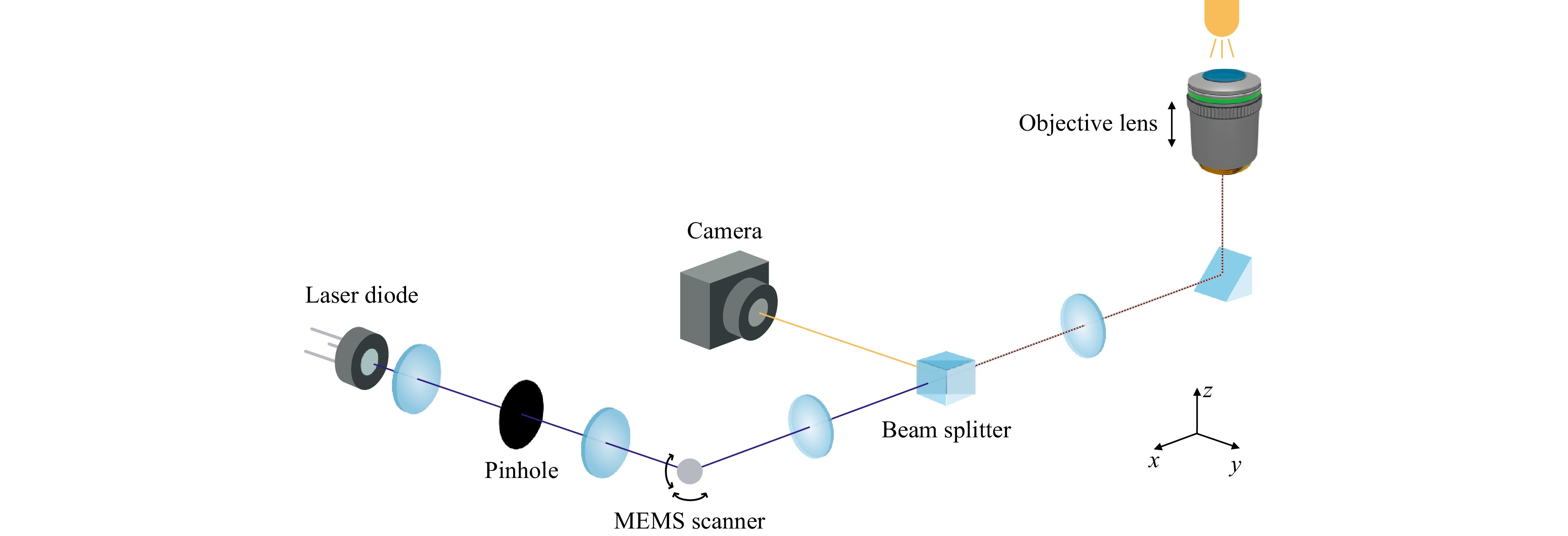
Fig. 1 Scheme of the optical setup forming the shoe-box-sized 3D laser nanoprinter. Starting with an inexpensive semiconductor laser diode with a housing diameter of only 3.8 mm, the divergent elliptical output beam at 405 nm wavelength is cleaned up by focusing through a 5 μm diameter pinhole. After collimation by a second lens, the laser beam is deflected by the 2D MEMS scanner for scanning arbitrary 2D trajectories. The scan and tube lens image the MEMS mirror onto the entrance pupil plane of the objective lens and enlarge the beam diameter. The high-NA microscope objective lens is mounted on a piezoelectric slip-stick stage for z-movement and focuses the laser beam into the liquid photoresist. Simultaneously, the objective lens collects the light from a transmission illumination. A compact camera allows to monitor the printing process.
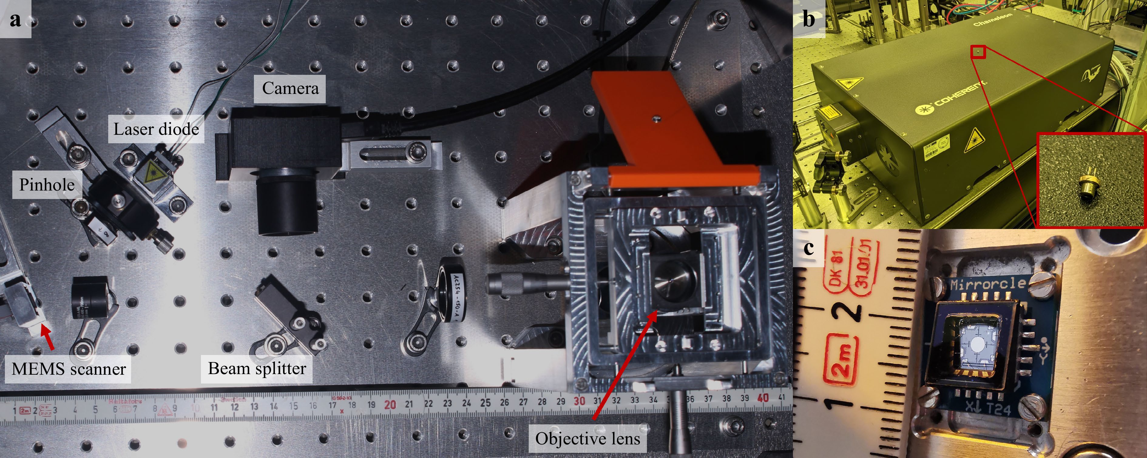
Fig. 2 Photographs of the entire optical setup and of selected crucial elements. a Optical setup with all components. A metric ruler is added at the side to provide a scale. Several further photographs of the setup taken from different shooting angles are depicted in Fig. S1. b Size comparison of the light sources used in two-photon lithography (large fs-pulsed laser oscillator) and in two-step lithography (small TO-38 can edge-emitting semiconductor laser diode). c Detailed view of the MEMS scanner with a metric ruler on the side. The TINY20.4 package with a footprint of 15 × 15 mm2 contains a wedged and AR-coated protection window, the mirror actuators, and the small aluminum-coated mirror with a diameter of 1.6 mm in the center.
Laser diodes additionally benefit from the direct modulation of the input current. This evades at no extra cost an additional component compared to state-of-the-art 3D laser nanoprinters, where expensive acousto-optic modulators are commonly used for power modulation and as high-speed shutters. The temporal response of the laser diode has been measured via an avalanche photodiode and a digital oscilloscope. The laser diode’s temporal response includes a constant delay time between the electronical output signal at the control unit and the actual optical signal, i.e., the emitted light. This delay of around 10 μs must be considered when synchronizing the power modulation and the focus scanning.
Another important element of a focus-scanning 3D laser nanoprinter is its scan unit. Two concurrent methods for the optical setup are easily employable: One possibility is to fix the entire optical path and to move the sample along the desired trajectory. This approach enables easy manufacturing of large structures without stitching due to a large print field. However, scan speeds are limited due to the mass that needs to be accelerated. In contrast, the mass involved when scanning the light by a rotatable mirror is much smaller. Here, we use mirrors rotatable around two orthogonal axes to scan the laser beam along the desired trajectory. However, a drawback of this approach lies in the limited print field, which cannot exceed the field of view of the used microscope objective lens. In this work, we employ a two-axis tip-tilt MEMS scanner (F1M16.2-1600AL, Mirrorcle Technologies, see Fig. 2c) with a mirror diameter of only 1.6 mm and an angular resolution of 0.6 mdeg for gimbal-less steering of the laser beam. The manufacturer specifies a surface roughness below 10 nm and a flatness corresponding to a radius of curvature larger than 5 m. In contrast to the commonly used galvanometric mirrors19, which benefit from extremely high-speed tilting around one axis, the two-axis MEMS scanner enables simultaneous deflection of the laser beam of up to 32° in both axes at fairly high speeds. Therefore, only a single scanning-mirror device is needed and, thus, no second lens system for imaging. Additionally, in contrast to driving galvanometric mirrors at full speed over extended periods of time, external cooling is not needed for such two-axis MEMS scanners as the internal electro-static actuators dissipate less than a few milliwatts at continuous full speed operation20.
The only 1.6 mm diameter of the mirror, however, obviously requires a correspondingly small beam diameter after the second lens and, thus, also small optical pathlengths between the elements due to the higher natural divergence of small beams. Beam diameter and collimation are measured by using a Shack-Hartmann wavefront sensor (WFS30-7AR/M, Thorlabs). We have been operating this device at its limits since the given minimum beam diameter for calculating certain Zernike polynomial orders is in the range of the desired beam diameter. The measured 1/e2 beam diameter of the collimated beam after the second lens is 1.67 mm, which means that we slightly over-illuminate the MEMS mirror.
The MEMS mirror is imaged by a scan lens (AC127-025-A-ML, Thorlabs) and a tube lens (AC254-150-A, Thorlabs) onto the entrance pupil of a vertically mounted microscope objective lens (HCX PL APO 100×/1.4−0.7 Oil CS, Leica Microsystems). The objective lens focuses the laser beam through a coverslip into a reservoir of the liquid photoresist. To utilize the full numerical aperture (NA) of the high-NA immersion microscope objective lens, a magnification of the beam diameter to the diameter of the entrance pupil of the objective lens via the scan and tube lens is necessary. The optical telescope needed for this magnification basically defines one of the outer dimensions of the shoe-box-sized 3D laser nanoprinter. Folding of the optical beam path would allow for further miniaturization. However, such folding would require additional components and would also make the alignment of the setup less convenient. A part of the length of the telescope is covered by the height of the microscope objective lens in the vertical part of the beam path. In principle, the vertical part could be extended to decrease the footprint of the device, albeit at reduced mechanical stability of the setup and increased instrument height.
For real-time monitoring of the printing process, the microscope objective lens not only focuses the 405 nm laser into the liquid photoresist, but also collects the transmitted light of a small light emitting diode (LED570L, Thorlabs) at 570 nm wavelength. A chromatic beam splitter (RGB-Strahlteiler, Lasertack GmbH) separates the collected light and the laser beam between scan and tube lens and deflects it on a small camera (Chameleon3, Teledyne FLIR). Additionally, the camera is used for finding the interface between substrate and photoresist. Here, the vanishingly small amount of 405 nm light reflected at the interface and deflected by the imperfect chromatic beam splitter is observed on the camera image. We note in passing that we have not observed instabilities of the laser diode due to the back-reflection from the interface reaching the laser diode. A software routine finds the smallest spot with highest brightness on the camera chip, while the objective lens is moved in small steps along the z-direction.
For this purpose, as well as for printing 3D rather than only 2D structures, the microscope objective lens is mounted on a compact linear piezoelectric slip-stick stage (LPS 30-30-1-V3_O-S-N, Nanos Instruments) with a travel range of 15 mm and a minimal incremental step size of 10 nm. The large travel range combined with small minimal incremental step size enables both coarse approaches of the sample as well as fine slicing during printing 3D structures using a single component. We emphasize that absolutely no additional stage for motions along the z-direction is used. The settings of the stage were optimized for position stability and fast step-settling for common slicing distances at the same time. A measurement of a typical 100 nm step pyramid is shown in Figure S3. The piezoelectric stage as well as the sample are mounted on a compact CNC-milled mount. Additionally, the sample can be moved in x- and y- direction by a self-designed manual stage employing micrometer screws for printing multiple structures on the same sample.
-
Although the optical setup for a stand-alone shoe-box-sized 3D laser nanoprinter is important, a compact control unit also requires careful consideration. Usually, the control unit consists of a rack full of controllers and a lab computer as a master. The full compact control unit is shown in Fig. 3. Here, the core element is a compact but powerful microcontroller (Teensy 4.1, PJRC). It is mounted on a home-made printed circuit board (PCB) together with additional electronic components. The microcontroller is the master of the control unit and serves as interface between lab computer and laser printing system.
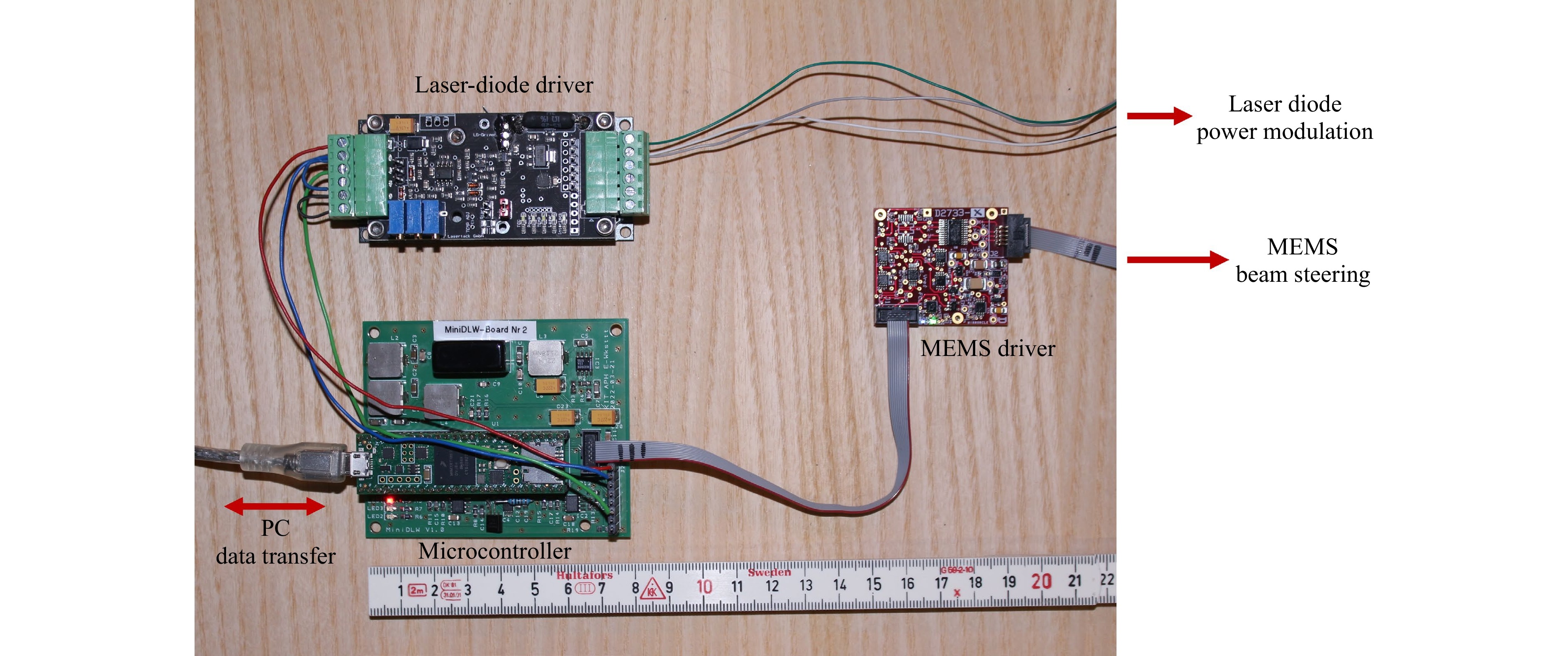
Fig. 3 Photograph of the control unit of the shoe-box-sized 3D laser nanoprinter. The microcontroller is mounted on a home-made printed circuit board (PCB). The PCB is connected to the PC via USB for data transfer, to the MEMS driver via SPI, and to the laser diode driver by cables. The laser-diode driver is directly connected to the edge-emitting semiconductor laser diode. It converts the input modulation voltage to the respective drive current for the laser diode for optical power modulation. The digital MEMS driver is directly connected to the TINY20.4 package of the MEMS scanner. It converts digital input signals from the microcontroller into the desired voltages for the mirror actuators for 2D beam steering. A metric ruler on the side allows to assess the sizes of the components.
For printing, a prepared job file containing all trajectories of the desired structure and a header with further information (e.g. print parameters, laser power, printing speed, etc.) is sent via USB to the microcontroller. All data are directly converted from absolute positions in the job file to the corresponding digital values for MEMS scanner control and buffered in the on-board memory. For larger 3D structures with lots of data points, additional external memory is mounted on the board. By sending the run command, printing of the loaded job starts and runs autonomously while certain feedback is sent back to the computer. With that, the microcontroller simultaneously outputs positions for the two-axis MEMS scanner and voltages for the optical laser diode output at a given update rate. In more detail, the Teensy 4.1 sends four digital values via SPI to the digital MEMS driver to address all four channels of the MEMS scanner (X+, X-, Y+, and Y-) for each position point. The digital-to-analog converter (DAC) on the digital MEMS driver further converts the four digital input values to the desired output voltages of 0–180 V for the actuators and applies them to the input pins of the MEMS scanner package.
At the same time, a digital value is output from the microcontroller to drive the laser diode for each position point. This digital value is converted to an analog voltage by a separate DAC on the home-made PCB and sent to a pin connector on the bottom right on the PCB. The corresponding pin is connected to the modulation voltage input of the laser-diode driver (PD-01359, Lasertack GmbH). The laser-diode driver is directly connected to the laser diode and translates the input modulation voltage to output the laser diode current for the current laser-focus position.
In addition, the 9 V supply voltage as well as the ground of the laser diode driver are connected to corresponding pins at the pin connector of the PCB and are provided by the microcontroller. We emphasize that this means that the full control unit of the shoe-box-sized 3D laser nanoprinter is powered by the 5 V USB connection of the microcontroller to the computer or a similar direct-current 5 V power supply for the microcontroller.
Besides the job file for printing, extra commands can be sent to the microcontroller to change certain preset parameters from their default value. These are, for example, the update rate, the conversion factors for distances in μm to the corresponding change of the MEMS scanner tilt angle, the default excitation laser power (if none is set explicitly in the job file), or the filter clock frequency for the desired filter cut-off frequency of the digital MEMS driver. Especially the latter is important to minimize the temporal delay between a new position output from the microcontroller and the voltage change at the digital MEMS driver output channels. A delay would otherwise lead to large deviations of the printed structure with respect to the design.
-
Among other structures, we decided for two demanding three-dimensional structures with special requirements to evaluate the printing performance of the shoe-box-sized 3D laser nanoprinter using the established photoresist system based on two-step photoinitiator benzil10. One is a chiral mechanical metamaterial unit cell21 with a dimension of 16 × 16 × 16 μm3 which has a fragile architecture and an extremely small filling fraction. The second is the #3DBenchy structure22 which is challenging due to its high filling fraction while, at the same time, containing additional fine features. Scanning electron micrographs of both structures are shown in Fig. 4, as evidence of good system performance. All fine features are nicely printed and although high filling fractions are challenging for the two-step resist system10, only a minor proximity effect can be observed at the boat's roof. Since after all, one of the main cost drivers of the shoe-box-sized 3D laser nanoprinter remains the high-NA microscope objective lens, further performance tests were conducted employing a 100× microscope objective lens with a slightly smaller NA of NA = 1.25 but which is more than an order of magnitude less expensive. Print results of a chiral mechanical metamaterial unit cell and a #3DBenchy structure are shown in Figure S4. There, it becomes visible that the axial definition of the microscope lens with NA = 1.25 is somewhat worse than the one with NA = 1.4 – as to be expected. Additionally, theoretical and experimental values for the point-spread-function of both microscope objective lenses are shown for comparison in Figure S5 and Figure S6.
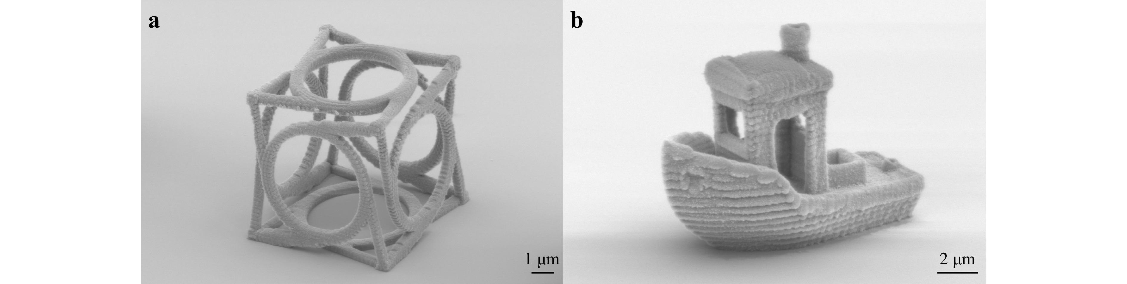
Fig. 4 Scanning electron micrographs of printed 3D structures. a One unit cell of a chiral mechanical metamaterial. b #3DBenchy structure. Both structures are printed with a scan velocity of 1 mms−1 and a hatching and slicing of 50 nm and 100 nm, respectively. The laser power used for the metamaterial unit cell is 700 μW and 400 μW for the #3DBenchy structure as measured at the entrance pupil of the microscope objective lens.
To thoroughly identify the resolution of the shoe-box-sized 3D laser nanoprinter, we additionally printed 2D line gratings and 3D woodpile structures23,24. Results are shown in Fig. 5. Line widths of 80 nm are easily achievable as deduced from the scanning electron micrographs. However, resolution is not defined by the smallest achievable line width but rather by the smallest distance of two parallel lines that are still separated23,25. The insets in Fig. 5a and Fig. 5b show that the lines are still separated for grating constants – and with that a lateral resolution – below 150 nm. This is in agreement with the results achieved employing the same microscope objective lens in our previous work using a bulkier setup10. Furthermore, also the axial resolution is investigated by printing 3D woodpile photonic crystals. Here, each layer is a 2D line grating where neighboring layers are rotated by 90° and the next-nearest neighboring layers are shifted by half of the grating constant26. Fig. 5c shows a top-view scanning electron micrograph of such a 3D woodpile photonic crystal with a side length of 20 μm, a lateral grating constant (or rod spacing) of 300 nm, and 24 layers. The zoom-in in Fig. 5d nicely shows the half-pitch shift of the subjacent next-nearest layer. Additionally, the lateral and axial voxel size can be derived from the oblique-view scanning electron micrograph in Fig. 5e as 80 nm and 275 nm, respectively. Again, the presented results match our previous results based on a bulkier setup10 and match with the spatial resolutions achieved by STED-inspired two-photon absorption at around 800 nm wavelength23.
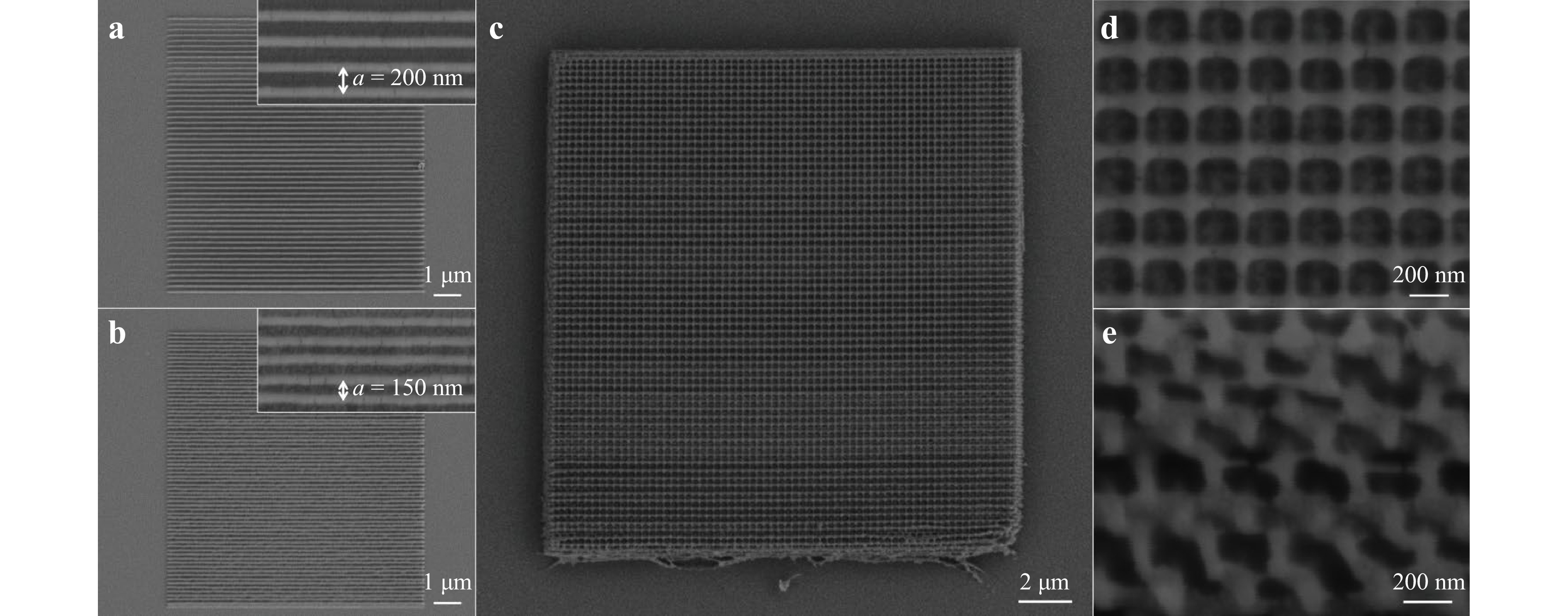
Fig. 5 Scanning electron micrographs of 2D line gratings and 3D woodpile structures. a 2D line grating with a side length of 10 μm and a grating constant of 200 nm and b a grating constant of 150 nm. Both insets are a zoom-in to show the separation of the lines down to a grating constant of 150 nm specifying the system’s lateral resolution. c Top-view scanning electron micrograph of a 3D woodpile structure with a side length of 20 μm and a lateral grating constant of 300 nm. The distance between two neighboring layers is 100 nm. d Zoom-in to the woodpile structure in c to show the nicely separated thin lines. With a half-pitch shift, the next-nearest neighboring layers can be seen in the gaps. e Oblique-view of the side of the woodpile structure to see again the separation of the single rods. The image can be taken to measure and calculate the dimensions of a single rod. The lateral voxel size can be derived as 80 nm and the axial voxel size as 275 nm. All structures are printed with a scan velocity of 0.1 mms−1 and a laser power of 120 μW.
To obtain good print results and good spatial resolution, the beam quality of the 405 nm laser diode is of major importance. Therefore, we have used a 5 μm diameter circular pinhole to clean up the elliptical beam shape as discussed above. To show the significance of the pinhole, we consider a starlike structure composed of 8 single lines rotated by an angle of 22.5° each. The results are shown in Fig. 6a (with 5 μm pinhole) and Fig. 6b (without pinhole). The linewidths were derived by the open-source image processing software Fiji and the corresponding pixel size of the scanning electron micrographs. We emphasize that the absolute thickness of the line is independent of the usage of a pinhole and rather depends on the used laser intensity as discussed earlier. However, it can nicely be observed that the linewidths do not vary as a function of the angle in presence of the pinhole, while they do vary significantly when removing the pinhole from the optical path. Fig. 6b suggests that the semi-major axis of the elliptical beam is roughly along the bisectrix of the third quadrant.
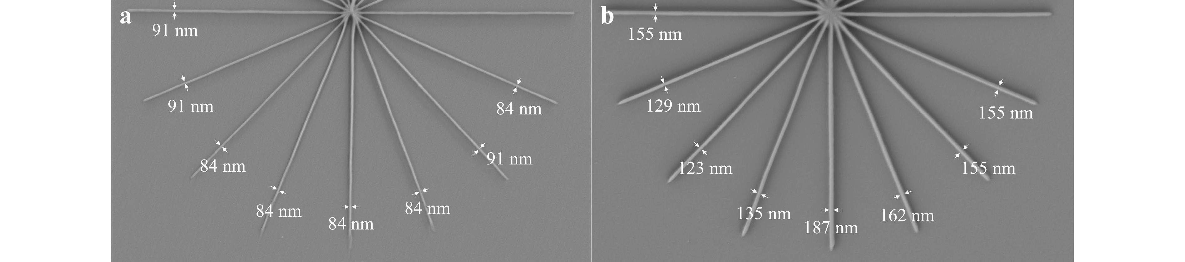
Fig. 6 Scanning electron micrographs of star-like structures when printing with (a) and without (b) a 5 μm diameter pinhole in the beam path. a No significant changes of the linewidths depending on the scanning direction are observable with the pinhole showing the quality of the clean-up of the elliptical beam shape emitted from the semiconductor laser diode. b The thickness of the lines changes with the scanning direction. The smallest linewidth of 123 nm at the bisectrix of the third quadrant suggests the direction of the semi-major axis of the elliptic beam shape. All linewidths are evaluated using the open-source image processing software Fiji. The laser power is 215 μW and 270 μW, respectively.
-
Two-step absorption instead of two-photon absorption as the excitation mechanism in 3D laser nanoprinting has emerged recently. Here, we use two-step absorption to arrive at a 3D laser printing machine tool that is drastically reduced in size and cost. We use an inexpensive low-power continuous-wave edge-emitting semiconductor laser diode as the light source instead of a bulky and expensive femtosecond-pulsed laser system. We further compact the remaining optical setup and especially the control unit to confine a fully functional high-resolution 3D laser nanoprinter in the volume of a shoe box. Our performance tests yield comparable performance with respect to our original work on two-step absorption. Using a low-cost $ \mathrm{N}\mathrm{A}=1.25 $ microscope objective lens, we estimate a total cost of all components of about five thousand Euros.
Further miniaturization as well as cost-cutting appear possible. The space assumed by the laser and the xy-scanning unit is already negligible. By folding the optical path, by replacing the bulky microscope objective lens by a solid-immersion lens, and by finding new approaches for the z-scanning, it appears possible to reduce the volume of the overall 3D nanoprinters to the scale of a fist and the cost to hundreds of Euros or US Dollars, respectively. Such an instrument could be powered by the USB-C port of a mobile telephone. It is our hope that the steps of miniaturization and cost-cutting will make the technology of 3D laser nanoprinting available to a yet much broader community.
-
The used photoresist is mixed strictly after the description of PR3 in Ref. 10. It contains 10.9 mg of Benzil as two-step photoinitiator and 12.9 mg of BTPOS as scavenger in 0.5 ml of TMPTA. The mixture is stirred for 24 hours. During the first 8 hours, the mixture was heated on a hotplate to 40℃. Benzil (98%) was purchased from SigmaAldrich. BTPOS (98%) was purchased from TCI Chemicals. TMPTA (93%) was purchased from Alfa Aesar.
-
All samples were developed for 2 min in spectroscopy-grade Acetone (CarlRoth GmbH), rinsed afterwards with spectroscopy-grade 2-Propanol (CarlRoth GmbH), and dried in a gentle stream of nitrogen.
-
We thank Vincent Hahn, Michael Thiel (Nanoscribe), and Matthias Blaicher (Nanoscribe) for discussions. We acknowledge funding by the Deutsche Forschungsgemeinschaft (DFG, German Research Foundation) under Germany’s Excellence Strategy for the Excellence Cluster “3D Matter Made to Order” (2082/1 – 390761711), by the Carl Zeiss Foundation, by the Helmholtz program “Science and Technology of Nanosystems”, by the Karlsruhe School of Optics and Photonics (KSOP), by the Max Planck School of Photonics (MPSP), and by Nanoscribe – A BICO company.
A shoe-box-sized 3D laser nanoprinter based on two-step absorption
- Light: Advanced Manufacturing , Article number: (2024)
- Received: 13 October 2023
- Revised: 02 May 2024
- Accepted: 12 May 2024 Published online: 09 July 2024
doi: https://doi.org/10.37188/lam.2024.027
Abstract: State-of-the-art commercially available 3D laser micro- and nanoprinters using polymeric photoresists based on two- or multi-photon absorption rely on high-power pico- or femtosecond lasers, leading to fairly large and expensive instruments. Lately, we have introduced photoresists based on two-step absorption instead of two-photon absorption, allowing for the use of small and inexpensive continuous-wave 405 nm wavelength GaN semiconductor laser diodes with light-output powers below 1 mW. Here, using the identical photoresist system and similar laser diodes, we report on the design, construction, and characterization of a 3D laser nanoprinter that fits into a shoe box. This shoe box contains all optical components, namely the mounted laser, the collimation- and beam-shaping optics, a miniature MEMS xy-scanner, a tube lens, the focusing microscope objective lens (NA=1.4, 100× magnification), a piezo slip-stick z-stage, the sample holder, a camera monitoring system, LED sample illumination, as well as the miniaturized control electronics employing a microcontroller. We present a gallery of example 3D structures printed with this instrument. We achieve about 100 nm lateral spatial resolution and focus scan speeds of about 1 mm/s. Potentially, our shoe-box-sized system can be made orders of magnitude less expensive than today’ s commercial systems.
Research Summary
Advancements in two-step absorption allow for shoe-box-sized 3D laser nanoprinters
A breakthrough in two-step absorption methodology revolutionizes 3D laser printing, offering a cost reduction of orders of magnitude compared to prevalent 3D laser nanoprinting systems. Leveraging a recently reported photoresist system based on two-step absorption and an economical continuous-wave semiconductor laser diode, this innovation redefines affordability in high-resolution manufacturing. Employing a compact MEMS xy-scanner coupled with a high-NA microscope objective lens enables a lateral spatial resolution of about 100 nm.
Rights and permissions
Open Access This article is licensed under a Creative Commons Attribution 4.0 International License, which permits use, sharing, adaptation, distribution and reproduction in any medium or format, as long as you give appropriate credit to the original author(s) and the source, provide a link to the Creative Commons license, and indicate if changes were made. The images or other third party material in this article are included in the article′s Creative Commons license, unless indicated otherwise in a credit line to the material. If material is not included in the article′s Creative Commons license and your intended use is not permitted by statutory regulation or exceeds the permitted use, you will need to obtain permission directly from the copyright holder. To view a copy of this license, visit http://creativecommons.org/licenses/by/4.0/.

 DownLoad: