


-
The manipulation of artificial micro/nanostructures to customize their inherent material characteristics has garnered considerable attention1–6. A diverse array of fields has blossomed, encompassing the creation of crystals with photonic band gaps4,5 and metamaterials by manipulating the effective primitivity and magnetic permeability1–3. Laser-induced structures and their wide-ranging applications across various fields have been extensively conducted for superhydrophobicity, anti-icing, and antireflection, as well as for industrial processes such as cutting and drilling7–10. Notably, an increasing number of experiments have not only validated the influence of structural morphologies on properties but also underscored how lasers impact performance by introducing extra stress, heat, and defects6,11,12. For example, femtosecond laser-induced black silicon exhibits superb absorption across the ultraviolet–infrared spectrum through the creation of quasi-periodic spikes12–14. However, the lifespan of non-equilibrium carriers in silicon is curtailed owing to surface roughness and defects stemming from intense interactions during structure formation6,14. In addition to the general refractive index change in the bulk, unique luminescent properties are changed by inducing the crystallisation of perovskite in the glass15,16. These promising results have gradually shown that, alongside the structural alteration, the inherent nature of the materials changes simultaneously. Significant strides have been made in fine-tuning structural properties through the development of models such as the dual-temperature, plasma, and structural feedback models17–22. However, less attention has been dedicated to material phase and element transitions. Furthermore, discourse on the mechanisms propelling molecular dynamics to facilitate these changes is lacking.
In this study, binary element decomposition was observed within laser-induced ripples on the surface of gallium arsenide (GaAs). This decomposition involved a substantial enrichment of arsenic (As) and a corresponding depletion of gallium (Ga) in proximity to the surface. Notably, selective stoichiometric compositions with As:Ga atomic ratios ranging from ~6:1 to 1:1 were successfully demonstrated to effectively activate the surface. This composition gradient exhibited a diminishing trend as the depth increased, inversely achieving an enrichment in Ga at approximately 350 nm and eventually reaching re-equilibrium after at least 7–9 μm. Comprehensive first-principles simulations revealed a pronounced propensity for phase separation within GaAs. Remarkably, the gasification of As–As bonds is more facile than that of Ga–Ga bonds, particularly beyond the melting point of GaAs. Consequently, under a pressure of 0.15 MPa, a remarkably high As:Ga atomic ratio of 14:1 was achieved. By leveraging the As-enriched surface, silver ions (Ag+) from an aqueous solution underwent a reduction reaction on the surface, leading to the creation of a distinctive metal-semiconductor hybrid surface. This innovation charted a pioneering course for surface chemical bonding applications and paved the way for enhanced detection through surface-enhanced Raman scattering (SERS). Because GaAs is one of the most important semiconductors for devices, such as photodetectors and integrated circuit chips, this breakthrough holds significant potential for advanced sensing and analytical applications23–25.
-
The As-enriched rippled surface was detected using X-ray photoelectron spectroscopy (XPS). Generally, laser-induced ripples can be categorised into near-subwavelength structures (NSWS), deep subwavelength structures (DSWS), and spikes as the pulse number and energies change19–21. NSWS primarily result from interference between the incident laser beam and scattered light, whereas DSWS involve surface plasmonic waves and even near-field effects. As shown in Fig. 1b, NSWS were only observed when scanning at a speed of 1.1 mm/s with a pulse energy of 20 μJ and a line interval of 50 μm. These structures appeared smooth, with small holes bound to the non-regular ripples. The holes grew deeper at a scanning interval of 20 μm (Fig. 1b2) and eventually transformed into spikes at a scanning interval of 5 μm (Fig. 1b3). Meanwhile, a second level of DSWS ripples emerged on top of the preformed NSWS, forming a hybrid structure (Fig. 1b3). As observed on other reported semiconductors, both the NSWS and the DSWS on the GaAs surface oriented themselves vertically to the laser polarisation11,19–21.
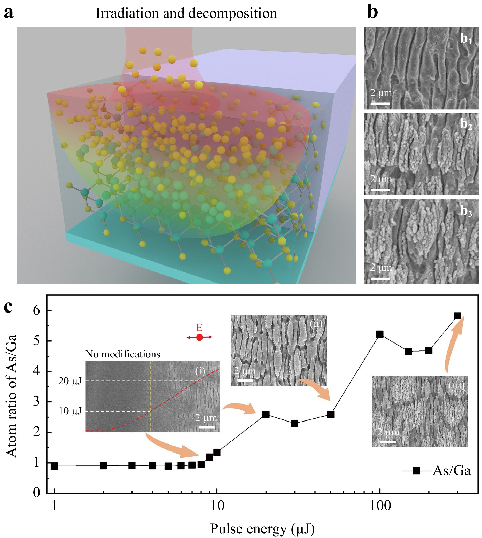
Fig. 1 (a) Schematic of femtosecond laser-induced irradiation and decomposition. The yellow and green spheres represent the arsenic (As) atoms and gallium (Ga) atoms, respectively. (b) Ripples formed at scanning intervals of 50 μm (b1), 20 μm (b2), and 5 μm (b3), respectively; (c) As:Ga atomic ratio on the surface at laser pulse energies ranging from 1 to 300 μJ. Inset scanning electron microscopy (SEM) images were obtained at pulse energies of 9 μJ, 50 μJ, and 300 μJ, respectively. The red arrow indicates the electron field of the laser beam.
The As:Ga atom ratio on the ripple surface was determined by the pulse energy, as shown in Fig. 1c. Four conclusions were drawn as the laser pulse energies varied from 1 to 300 μJ. First, when the pulse energies varied from 1 to 8 μJ, which was far below the ablation threshold of approximately 20 μJ, the As:Ga atomic ratio was approximately 0.9. This value was the same as that of the bulk GaAs without laser irradiation, and no mass removal occurred. In general, the XPS analysis used for the relative composition of the constituents in the surface region usually has 10% uncertainty, which could explain why the ratio is not 1:1. Second, when the pulse energy varied from 9 to 12 μJ, the surface morphology hardly changed, according to the SEM images (the left inset images in Fig. 1c). However, the stoichiometric decomposition of GaAs occurred, and the As:Ga atom ratio rapidly increased to 1.4. Third, the ratio increased when the pulse energy varied from 20 to 100 μJ, indicating that more Ga–As bonds broke in the bulk and that As atoms fled toward the surface. At this stage, a femtosecond laser-induced NSWS was observed, as shown in the middle inset of Fig. 1c. This was attributed to the interference between the incident light and the laser-induced surface wave. Last, when the pulse energies were higher than 100 μJ, the As:Ga atomic ratio saturated at a value of approximately 6:1. Notably, DSWS was formed on top of the NSWS, which involved intense interference between the surface plasmonic wave and the incident laser beam20.
-
Binary decomposition involves the following steps: light absorption, binary decomposition via bond breaking, and mass removal via thermal effects. A schematic of binary decomposition is illustrated in Fig. 2a, where the As:Ga atomic ratio changed significantly from the surface to the inner parts of the ripples. To confirm this, an argon ion beam etching was employed to investigate the atomic ratio in the depth profiling of the ripples irradiated by a 150 μJ pulse. The inset of Fig. 2b shows a cross-sectional SEM image of the structural surface. The height of the structure is denoted as H1 = 4 μm, and a maximum depth of H2 = 9 μm was milled for XPS detection. The atomic ratio at the surface was approximately 4.5 (indicating an As-enriched surface, labelled I). This value decreased significantly with depth and gradually stabilised to 0.9 at a depth of approximately 350 nm (representing the As-enriched bulk region, labelled II). Afterward, the value decreased slightly and eventually returned to 0.9 until a depth of approximately 7–9 μm, indicating the As-depleted/Ga-enriched bulk region, labelled III). The value remained consistent with the unmodified region after a depth of 9 μm (representing the original state, labelled as IV). During these processes, transmission electron microscopy (TEM) and high-resolution transmission electron microscopy (HRTEM) images26 revealed that the lattice was relatively reshaped and that a layer fault occurred at the upper right corner (Fig. 2b1, b2) compared with the unexposed region at the lower left corner (Fig. 2b1, b3).
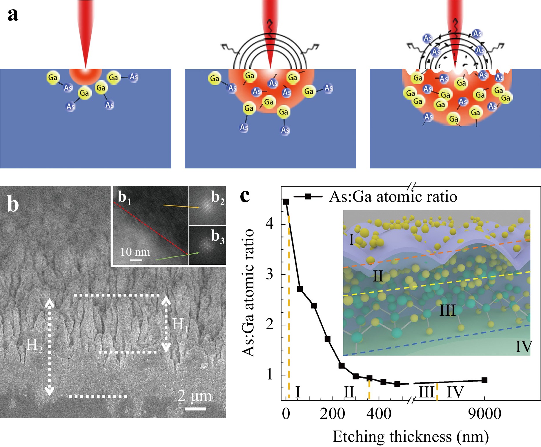
Fig. 2 (a) Schematic of the laser-induced binary decomposition of GaAs. (b) Cross-sectional profile of ripples. The inset in (b1) shows a HRTEM image of the sample. (b2, b3) show HRTEM images of the exposed and unexposed regions, respectively. (c) As:Ga atomic ratio at a depth of 0–9 μm and pulse energy of 150 μJ. The inset shows a schematic diagram of element decomposition with regions from I to IV.
-
Considering that Ga (melting point of 29.8 °C) possesses a significantly lower melting point than As (817 °C)27,28, Ga is expected to be the primary constituent that escapes during the ablation process. The closer they are to the surface, the more Ga atoms are likely to escape from the bulk to the air. This hypothesis is valid when considering that all the modified regions along the cross-section are enriched in As, as depicted in Fig. 2b. However, this hypothesis does not explain the presence of enriched Ga states in deeper bulk regions.
To explain the mechanisms underlying binary elemental decomposition, a theoretical first-principles molecular dynamic was implemented using the Vienna Ab-initio Simulation Package (VASP) codes with the generalised gradient approximation (GGA)29. The electron-ion interaction was described by the frozen-core all-electron projector augmented wave (PAW) method29,30. Typically, when an ultrafast laser pulse (e.g. several hundreds of fs) is exposed to a solid material, it undergoes two primary processes: i) electronic excitation to disturb the atoms locally within the first several picoseconds and ii) a heating effect, including ablation (or evaporation, thermal diffusion, or plasma), due to available electron–hole (e–h) recombination, usually at >100 ps. In particular, when the laser fluence was sufficiently high, the heating effect occurred even earlier.
In the current experiment, we conclusively identified that the observed ablation and phase separation resulted from the thermal effects induced by single-photon absorption (the photon energy of 1.55 eV at a wavelength of 800 nm versus the GaAs band gap of 1.4 eV). The thermal relaxation time of GaAs, denoted τ0, is proportional to δ2/α, where δ is the structure depth H1 of approximately 5 μm and α is the thermal diffusivity of approximately 0.2–0.4 cm2s−1, as measured by photothermal deflection spectroscopy31–35. The thermal relaxation time τ0 was measured in microseconds (10−6 s). During the heating process, the temperature was estimated from T0 = PE(1-R)/2cρV ≈ 3000 K at a pulse energy (PE) of 150 μJ, where R is the surface reflection of 33% at a refractive index of 3.68 at 800 nm, ρ is the mass density of 5.32 g/cm3, c is the specific heat capacity of 0.325 J/g/K, and V is the ablation volume estimated by a focus diameter of D = 2fλ/D0 = 37 μm and an absorption height (modification height H2) of approximately 9 μm (measured from Fig. 2b). Because the pulse interval time τR (1 ms at a repetition rate of 1000 Hz) is much larger than τ0, the thermal accumulation between pulses could be neglected. That is, each pulse must be sufficiently energetic to cause an ablation/explosion and jets with a “hot process” above the material boiling/sublimation temperature. On one hand, the effective absorption volume (diameter and focal length) decreased accordingly at lower pulse energies. On the other hand, larger scatterings at higher pulse energies ensured that the absorbed part was saturated20. A temperature of approximately 3000 K is representative of pulse energies higher than the threshold of 20 μJ.
To understand the physical origin of the As-rich surface, we performed first-principles molecular dynamics to evaluate the phase stability of GaAs by laser ablation. Fig. 3a summarises the proximate phase map of GaAs and its two elements in three temperature districts. The As atom at 886 K sublimed directly from the solid without going to the liquid, whereas the Ga atom existed as a liquid from 303 to 2676 K. Fig. 3b shows the local structure of crystalline (at 300 K) and diffusive (at 1600 K) GaAs based on a partial correlation function analysis with molecular dynamics. Notably, only Ga–As bonds existed in the crystal, as reflected by the first neighbouring peak of the Ga–As pair. In contrast, when the temperature of GaAs exceeded its melting point, considerable amounts of Ga–Ga and As–As bonds were observed in the diffusive state. That is, the liquid state of GaAs exhibited a strong tendency for phase separation. Combined with the discussion of the phase map above, As was immediately gasified after melting GaAs. Taking 3000 K as an example, both the Ga and As atoms were gasified. However, the diffusion of Ga atoms rapidly decreased below 2676 K, and the As atoms kept moving from the bulk to the surface until the temperature was below 886 K. Regarding the decomposition at the pulse energy below 20 μJ, for example, 10 μJ, the temperature at the focus centre must be slightly higher than the melting point of GaAs at 1511 K to allow only the gasification of As atoms and the melting of Ga atoms.
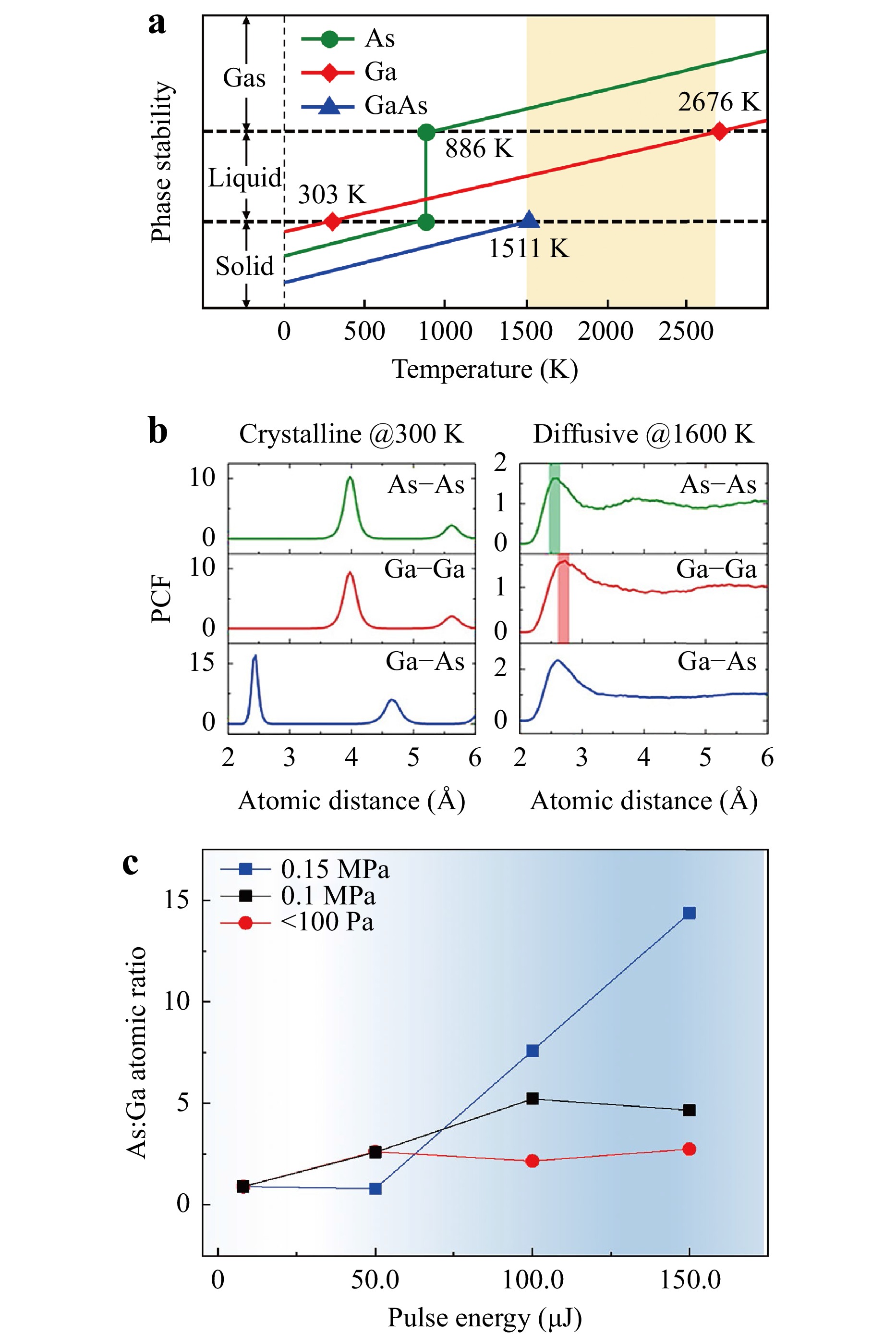
Fig. 3 Origin of phase separation. (a) Schematic of phase stability for GaAs and its elements. The yellow-shaded drawing highlights the temperature region of phase separation. (b) Atomic pair correlation functions from the first-principles molecular dynamics reflect the obvious formation of As–As (green-shaded) and Ga–Ga (red-shaded) bonds above the melting point of GaAs. (c) As:Ga atomic ratio with pulse energies at different air pressures. The red, black, and blue curves correspond to the As:Ga atomic ratio with pulse energies under 100 Pa, 0.1 MPa, and 0.15 MPa, respectively.
To further substantiate this hypothesis, experiments were conducted at different atmospheric pressures. Fig. 3c shows that the As:Ga atomic ratio on the wafer remained nearly constant at pressures of 100 Pa, 0.1 MPa, and 0.15 MPa when the pulse energies were slightly below the threshold. However, at a laser pulse energy of 50 μJ, a noticeable increase in gasified As migrating from the bulk toward the surface was observed. This migration resulted in the formation of an As-enriched surface at pressures of 100 Pa and 0.1 MPa. In Fig. 3b, this ratio exhibits an initial increase, reaching a value of 2.62, before stabilising at approximately 2.5 at a pressure of 100 Pa. At 0.1 MPa, the ratio initially increased to 2.59 and continued to increase until it reached saturation at approximately 5. Interestingly, there was no discernible change at a pressure of 0.15 MPa, even though the laser ablation threshold increased. No significant changes were observed under these conditions. However, at higher laser pulse energies, such as 100 μJ, the As:Ga atom ratio exhibited a significantly higher value of 7.59, in stark contrast to the values of 2.16 at 100 Pa and 5.22 at 0.1 MPa. At 150 μJ, the ratio reached 14.4, which is three times that observed at 0.1 MPa and five times that recorded at 100 Pa.
According to the Ideal Gas Law (PV = nRT) and Charles’ Law (P/T = C), a higher air pressure P results in a higher melting/boiling/sublimation point T, and the inverse case is also true. More, the higher air pressure will significantly decrease the escaping speed from the subsurface. This implies that more As atoms gather below the surface at a higher pressure. The Ga atoms probably maintain their original positions owing to a two-step transition from solid to liquid and then liquid to gas. (Fig. 3a) Therefore, the As:Ga atomic ratio will increase at a higher air pressure, and, inversely, it will decrease at a lower air pressure. All these results were found to be inconsistent with speculation that As atoms were the main “escape” element from the surface during laser ablation.
-
GaAs wafers have been used for the direct synthesis of Ag nanoplates through a simple solution/solid interfacial reaction strategy36–38. In this method, the primary source to reduce Ag+ to silver structures is As, which can be selectively activated by a femtosecond laser. Thus, it holds immense promise for achieving a more efficient and controllable synthesis of Ag structures via simple laser direct writing. Fig. 4a outlines the fabrication process, which involves laser ablation and silver reduction processes, for the silver-semiconductor hybrid coating. As shown in Fig. 4b1, a five-petal silver nanostructured pattern with a diameter of 500 μm was fabricated. The magnified SEM image revealed a compacted pattern of Ag nanoplates in the “laser-activated” region and a low areal density of scattered nucleation sites in the unexposed region. Fig. 4b2 showed a pattern of an 8 × 8 “H” character array that demonstrated flexibility for arbitrary design texturing via laser direct writing technology. The difference in reduction depended on the content of As atoms on the surface, which played the role of a reactant, transferring electrons to silver ions for the silver structures. This process differs from the GaAs-mediated reduction of Ag+ ions, which is elaborated below37.
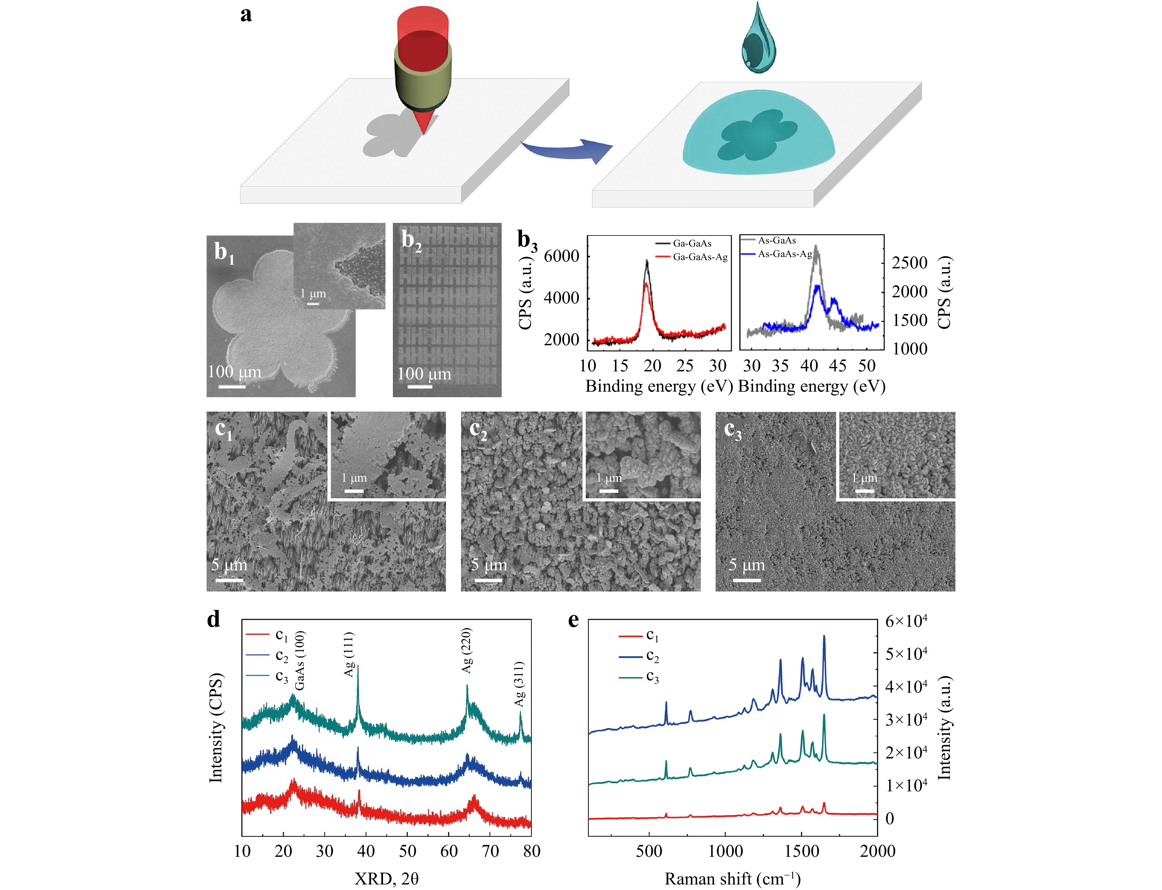
Fig. 4 Selective activation and SERS applications. (a) Schematics of laser selective surface activation and the reduction of silver. (b1) SEM images of the laser-activated silver region. (b2) Laser-activated “H” array with reduced silver. (b3) XPS spectra of As before and after the reduction of silver. (c1–c3) Ag nanostructures under reaction times of 20 s, 40 s, and 60 s on the equivalent As-rich GaAs wafers. (d) XRD of the hybrid Ag/GaAs structure in (c1–c3). (e) SERS spectra of Rhodamine 6G molecules detected on the substrate of (c1–c3) with a concentration of 10−9 mol/L.
$$ \begin{array}{c}\rm 12AgNO_3+2GaAs+6H_2O \to 12Ag+Ga_2O_3 + \\ \rm As_2O_3 + 12HNO_3 \end{array} $$ (1) XPS analysis unequivocally confirmed that only As exhibited changes in its valence state following the reduction of Ag+ ions, as shown in Fig. 4b3. The reduction process yielded distinct silver nanostructures based on the reaction time. At a reaction time of 20 s, the primary product consisted of silver nanobelts (Fig. 4c1). Extending the reaction time to 40 s resulted in the formation of large silver nanoplates (1 μm) interspersed with smaller, densely packed nanoplates (200 nm) (Fig. 4c2). When the reaction time reached 60 s, closely packed nanoplates (200 nm) were formed (Fig. 4c3). Shorter reaction times yielded larger and thinner nanostructures, consistent with the X-ray diffraction (XRD) data, as illustrated in Fig. 4d. The (100) crystal orientation peak of the laser-structured GaAs broadened and decreased compared with the original state, which was attributed to the presence of defects and the blanketing effect of the Ag structures. These changes in the XRD data suggest that the Ag nanobelts that formed in a short time were single crystals oriented along the (111) direction. In contrast, the long-term formation of both individual and packed nanoplates results in multicrystalline structures encompassing phases such as (111), (220), and (311).
To demonstrate its potential application, we designed an experiment centred on the surface-enhanced Raman scattering test and subsequently assessed the SERS activity of the silver nanostructures. We chose Rhodamine 6G as the probe molecule, and the detection limit could reach 10−9 mol/L when utilising the hybrid structured surface (NSWS and DSWS) shown in Fig. 1b. This result aligns with the concept that a thicker layer of plasmonic metal corresponds to a proportionally stronger SERS signal, with an enhancement factor of up to 108 39–41. Both surface roughness and nanointerstices play pivotal roles in augmenting the local electric field of light, contributing to the enhancement observed in the SERS response. Even though the single smooth crystal nanobelt exhibited slightly lower SERS performance compared with the nanoplates, it still achieved a commendable detection sensitivity of 10−9 mol/L.
-
The binary decomposition of GaAs induced by femtosecond laser irradiation has been comprehensively investigated and reported. During this process, gasified As inversely diffused along the incident laser direction, leading to an elevated As:Ga atomic ratio. Consequently, the As:Ga atomic ratio was the highest at the surface, with the ratio gradually decreasing as the depth increased to 350 nm. The ratio inversely achieved an enrichment in Ga at approximately 350 nm, and it eventually reached re-equilibrium after at least 7–9 μm. Further in-depth exploration conducted through first-principles molecular dynamics simulations revealed a distinctive bond-breaking phenomenon involving Ga–As bonds above the melting point of the material. This process was followed by the reformation of Ga–Ga and As–As bonds. These findings indicate that As was promptly gasified, a conclusion corroborated by controlling the As:Ga atomic ratio via air-pressure manipulation. Specifically, lower pressures (100 Pa) yielded reduced As:Ga atomic ratios, whereas higher pressures (0.15 MPa) led to significantly elevated atomic ratios. By leveraging the selectively activated As-enriched surface, it was possible to use it as a reducing agent for Ag in SERS applications. The proposed laser-induced selective activation technique for GaAs can be extended to other binary semiconductors such as gallium nitrate and the controlled growth of Pd and Au/Ag alloys via galvanic reactions, thereby paving the way for new opportunities in surface chemical bonding, solar cell technologies, and sensing and detection applications.
-
GaAs samples (Beijing Zhongke Jiaying Semiconductor Co., Ltd.) were cleaned with acetone, ethanol, and deionised water. Laser structuring was then performed using a Ti:Sapphire laser at a wavelength of 800 nm, pulse duration of 100 fs, and repetition rate of 1000 Hz. The pulse energy was conducted from 10 to 300 μJ with a diameter of 10 mm. A lens with a focal length of 600 mm was used for large-area fabrication for XPS detection, and an objective lens (50×, NA 0.5) was used for micropatterning. Polarisation was controlled by a half-wave plate, in which ripples were formed with an orientation perpendicular to the E-field of the laser.
-
Selective activation for SERS includes three steps: i) laser ablation of the GaAs wafer to create the desired pattern (Fig. 4a, b); ii) cleaning the pattern with a hydrofluoric acid solution (HF solution, 5 mol/L) for 1–5 min to remove surface oxidation; and iii) immersing the structured GaAs into a silver nitrate solution (AgNO3 solution, 0.01 mol/L) for tens of seconds and then rinsing the pattern with distilled water.
-
The morphologies of all samples were measured by SEM (JEOL JSM-6700F). The As:Ga atomic ratio was determined by XPS using an ESCALAB 250 spectrometer (Thermo Scientific). To detect the atomic ratios at different depths, integrated argon ion beam etching, which does not affect the atomic ratio, was used to remove the materials. A RigakuD/Max-2550 diffractometer was used for the XRD measurements. TEM and HRTEM were performed using a JSM-2100 (JOEL). A JOBIN YVON T64000 equipped with a liquid nitrogen-cooled argon ion laser (514.5 nm) was used for the surface-enhanced Raman spectra SERS.
-
An energy cut-off of 250 eV was used for the plane-wave expansion. A 96-atom GaAs supercell was employed for all calculations. In the molecular dynamics simulation, one point was used for Brillouin zone sampling. We used a 3 fs time step and the canonical NVT (N for a constant amount of matter, V for a constant volume, and T for a constant temperature) ensemble, in which a Nosé–Hoover thermostat was used to control the temperature. To obtain a reasonably diffusive state of GaAs, we first heated the crystal at a sufficiently high temperature of 3000 K for 6 ps to completely lose the long-range order, and we then annealed it to 1600 K (which was slightly above the melting point) for another 18 ps. We used the last 3 ps to evaluate the atomic structure of this diffusive state of GaAs.
-
The Key R&D Program of Shandong Province (2021CXGC010201), National Natural Science Foundation of China (61827826, 62175086, 62205024), and Natural Science Foundation of Jilin Province (20220101107JC). All the authors thank Prof. Saulius Juodkazis and Prof. Hong-Bo Sun for their valuable discussions and advice on draft preparation.
Ultrafast laser-induced decomposition for selective activation of GaAs
-
Ke-Mi Xu1, 2,
 ,
, - Chao Liu1,
- Lei Wang2, *, ,
- Feng-Chun Pang2,
- Xin-Jing Zhao2,
- Xian-Bin Li2,
- Qi-Dai Chen2,
-
Wei-Qian Zhao1,
- Light: Advanced Manufacturing , Article number: (2024)
- Received: 05 September 2023
- Revised: 23 April 2024
- Accepted: 24 April 2024 Published online: 29 June 2024
doi: https://doi.org/10.37188/lam.2024.026
Abstract: The manipulation of micro/nanostructures to customise their inherent material characteristics has garnered considerable attention. In this study, we present the selective activation of gallium arsenide (GaAs) via ultrafast laser-induced decomposition, which correlates with the emergence of ripples on the surface. This instigated a pronounced enrichment in the arsenic (As) concentration around the surface while inducing a depletion of gallium (Ga) at the structural depth. Theoretical simulations based on first principles exhibited a robust inclination towards the phase separation of GaAs, with the gasification of As–As pairs proving more facile than that of Ga–Ga pairs, particularly above the melting point of GaAs. As an illustrative application, a metal-semiconductor hybrid surface was confirmed, showing surface chemical bonding and surface-enhanced Raman scattering (SERS) through the reduction of silver ions on the laser-activated pattern. This laser-induced selective activation holds promise for broader applications, including the controlled growth of Pd and the development of Au/Ag alloy-based platforms, and thereby opens innovative avenues for advancements in semiconductors, solar cell technologies, precision sensing, and detection methodologies.
Rights and permissions
Open Access This article is licensed under a Creative Commons Attribution 4.0 International License, which permits use, sharing, adaptation, distribution and reproduction in any medium or format, as long as you give appropriate credit to the original author(s) and the source, provide a link to the Creative Commons license, and indicate if changes were made. The images or other third party material in this article are included in the article′s Creative Commons license, unless indicated otherwise in a credit line to the material. If material is not included in the article′s Creative Commons license and your intended use is not permitted by statutory regulation or exceeds the permitted use, you will need to obtain permission directly from the copyright holder. To view a copy of this license, visit http://creativecommons.org/licenses/by/4.0/.

 DownLoad: