


-
In recent years, rapid advancements in technologies such as the Internet, mobile communications, Internet of Things, and artificial intelligence have led to an exponential growth in communication connections between devices, the number of devices, and communication terminal connections1–3. Consequently, the demand for improved communication rates and capacities has increased progressively. Over the past few decades, optical communication technologies led by fibre-optic communication have replaced wired cable-based communication and become the mainstream approach4–6. Utilising multiple dimensions of photon, researchers have introduced techniques such as wavelength-division multiplexing7–11, mode-division multiplexing (MDM)12–15, polarisation-division multiplexing16–19, and time-division multiplexing20–22 to enhance communication capacity. Among these, MDM enables the utilisation of various spatial modes, such as linear polarisation (LP)23,24, orbital angular momentum (OAM)25–27, and vector modes28–30. The OAM mode, which possesses unique characteristics31,32, has gained considerable attention as a focal point in MDM research and found widespread applications in both free-space optical communications33–36 and fibre-optic communications37–39. With the continuous advancements in optical fibre technology, various fibres supporting high-order modes, such as few-mode, multimode, and hollow-core fibres, have been developed and are gradually being deployed commercially, forming multimode optical communication networks. However, in multimode optical communication networks, information transmission requires processing at the network nodes, such as optical switching, which is crucial for data information management and flexible scheduling in optical communication networks. Traditional optical switching networks face compatibility issues when dealing with higher-order modes because they are primarily designed for mainstream single-mode fibre networks. To address optical switching among higher-order modes, sophisticated solutions are often required, such as the incorporation of fibre gratings40 and spatial light modulators41,42. However, the devices in these solutions have larger volumes and exhibit limited flexibility and response time.
Photonic integration technology is crucial for the advancement of high-speed optical communications and has been extensively incorporated into various components of high-speed optical communication systems43,44. It has fuelled the rapid development of on-chip optical switching45–47, with devices based on microring resonators (MMR)48,49 and Mach-Zehnder interferometers (MZI)50,51 serving as building blocks for large-scale optical switch networks. These optical switching networks utilise photonic integration technology, which enables the realisation of highly integrated and rapidly responsive optical switching chips52. The latest network configurations have dimensions as large as 128 × 12853, which demonstrates remarkable levels of integration and scale. Additionally, optical cross connects based on microelectromechanical systems (MEMS) can achieve low-loss and large-scale optical switching networks54–56. However, these optical switches require predefined configurations for different exchange states, lacking intelligent configurability. In practical applications, optical chips may experience thermal crosstalk owing to environmental temperature variations and differences between various phase shifters. This can increase crosstalk among different channels and degrade communication performance, thereby making automatic adjustment unattainable. The optical neural network architecture has emerged as a novel biomimetic structure with promising improved parallel functionality, enhanced device performance, and greater scalability for optical switching57–59. On-chip integrated optical neural networks primarily involve MZI arrays60,61, MRR arrays62, and multiple-plane light conversion63. These on-chip integrated optical neural networks have demonstrated capabilities in vowel recognition64, image recognition65–68, and MIMO descramblers69–72 and significantly enhance the processing potential of photonic chips. By leveraging neural network architectures, we propose to transform the on-chip integrated photonic switch structure to achieve more flexible switching, fault tolerance, and power efficiency. We foresee the possibility of achieving extensive parameter learning and performance optimisation by optimising the parameters of the on-chip integrated neural networks using algorithmic approaches.
This study introduces and demonstrates a flexible mode-switching system based on an optical neural network chip. We integrated an optical neural network chip and all-fibre OAM mode (de)multiplexer to establish an adaptive and versatile optical switching configuration tailored to the OAM modes. We designed a 4 × 4 silicon-based optical neural network chip in a rectangular network framework. Using an improved gradient descent algorithm, we trained 3 × 3 arbitrary switching states. We experimentally verified the fibre–chip–fibre optical exchange system by selecting orthogonal zeroth-, first-, and second-order OAM modes in a multimode fibre and loading different modulation signals. This implementation of a flexible mode-switching system holds promise for applications in multimode fibre MDM optical communication systems.
-
Fig. 1 shows a schematic of mode optical switching based on a photonic neural network chip. We built a self-configurable mode optical switching network by combining a photonic neural network chip with a multimode fibre. The channels in the multimode fibre represent mode channels, where different data information is modulated in different orthogonal modes for multiplexed transmission. Multiple mode channels within the input multimode fibre were first demultiplexed into single mode fibres using a mode demultiplexer. These single-mode fibres were connected to a photonic neural network chip to achieve multichannel optical switching. Subsequently, the signals passed through the single-mode fibres and were multiplexed back into multimode fibres using a mode multiplexer. This process facilitated the exchange of data in multiple mode channels within the multimode fibre.
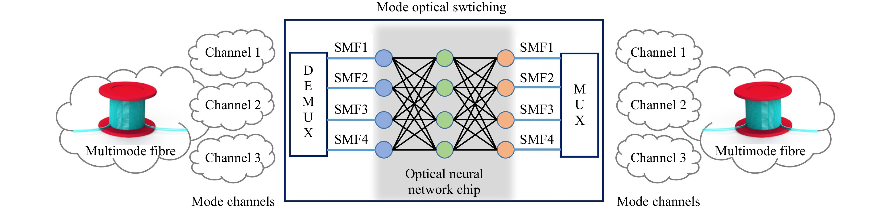
Fig. 1 Conceptual diagram of mode optical switching. DEMUX: Demultiplexer; SMF: Single-mode fibre; MUX: Multiplexer.
The photonic neural network chip consisted of an N×N interferometric network. Currently, two mainstream configurations, namely, the triangle53 and rectangular52 network frameworks, are used. We chose the rectangular network because of its shorter interference depth. This allows for better balancing of losses in different paths, which make it more suitable for the optical switching applications in this study. As shown in Fig. 2a, the 4 × 4 interferometric network can be decomposed into MZIs with 2 × 2 configurations. Each MZI consists of two 3-dB couplers and two phase shifters, which are controlled by parameters φ and θ and represented by a 2 × 2 unitary transformation matrix as described by the following equation:
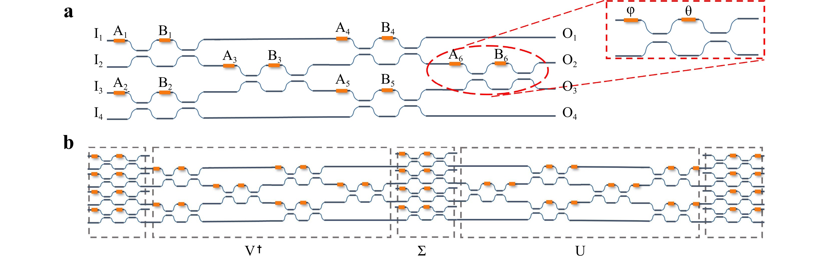
Fig. 2 a Configuration of the 4 × 4 universal unitary network. b Configuration of the 4×4 universal linear network.
$$ {U}_{MZI}=\frac{1}{2}\left[\begin{array}{cc}{e}^{i\varphi }({e}^{i\theta }-1)& i\left({1+e}^{i\theta }\right)\\ {ie}^{i\varphi }\left({1+e}^{i\theta }\right)& 1-{e}^{i\theta }\end{array}\right] . $$ (1) According to the scheme proposed by Clements et al.52, arbitrary 4 × 4 unitary matrix transformations can be achieved by arranging six MZIs as shown in Fig. 2a. To implement arbitrary 4 × 4 linear matrices, we can use the singular value decomposition method to obtain
$$ M=U\Sigma {V}^{\text †} $$ (2) The network schematic is shown in Fig. 2b, and it comprises two unitary matrix networks and a diagonal matrix. The layout shown in Fig. 2b was chosen as the chip layout to achieve more powerful functionalities. In Fig. 2b, the leftmost and rightmost sets of the eight MZIs modulate the output amplitudes of the different channels, ensuring an overall balance in the optical intensity for convenient testing in practical experiments. The entire network consisted of 16 MZIs acting as nodes. Each node was controlled by a phase shifter that served as an adjustable parameter within the network. Various matrix configurations were obtained by applying distinct phase shifts to the shifters across the network.
In our experiment, we used the orthogonal zeroth-, first-, and second-order OAM modes. These three OAM modes were generated and multiplexed using a cascaded all-fibre (de)multiplexer. The process was initiated by exciting the left-hand circularly polarised light in a single-mode fibre, which was decomposed into the $ {HE}_{11}^{x} $ and $ {HE}_{11}^{y} $ modes with a phase difference of $ {\text π}/{2} $. Through appropriate tapering and fusion splicing, these modes were coupled to generate the $ {HE}_{21}^{e} $and$ {HE}_{21}^{o} $ modes in the multimode fibre, which introduced a phase difference of ${\text π }/{2} $. Similarly, the$ {HE}_{31}^{e} $ and $ {HE}_{31}^{o} $ modes were created in the multimode fibre with a phase difference of $ {\text π }/{2} $ by coupling via suitable tapering and fusion splicing, thus forming the second-order OAM mode. Our all-fibre OAM mode (de)multiplexer incorporates a standard single-mode fibre (SMF-28) and conventional multimode fibre (OM3). We indicate the phase-matching points through simulations aimed at determining the refractive index distribution of the modes at various radii, as illustrated in Fig. 3a, b. We pre-tapered the single-mode fibre to ensure that the effective refractive index of the fundamental mode matched the required orbital angular momentum mode in the multimode fibre. After determining the processing parameters through theoretical simulations, we used the melt-tapering method to fabricate an all-fibre OAM-mode (de)multiplexer. We used a moving hydrogen-oxygen flame to pre-taper the single-mode fibre diameters to 77 μm and 55 μm, thereby satisfying the phase-matching conditions for coupling from the fundamental mode to OAM+11 and OAM+21. Subsequently, a fixed flame was used for the simultaneous melt-tapering of the pre-tapered single-mode and the multimode fibres. A power meter was used to monitor the power at both output ends of the coupler in real-time to ensure maximum coupling efficiency of mode conversion. The generation of the OAM01 mode does not require a complex tapering process; a high-purity OAM01 mode can be excited by simply splicing the SMF with OM3. We obtained a three-channel all-fibre OAM mode generator and multiplexer (Fig. 3c) by cascading these processes. Similar principles can be applied to obtain an all-fibre OAM mode demultiplexer.
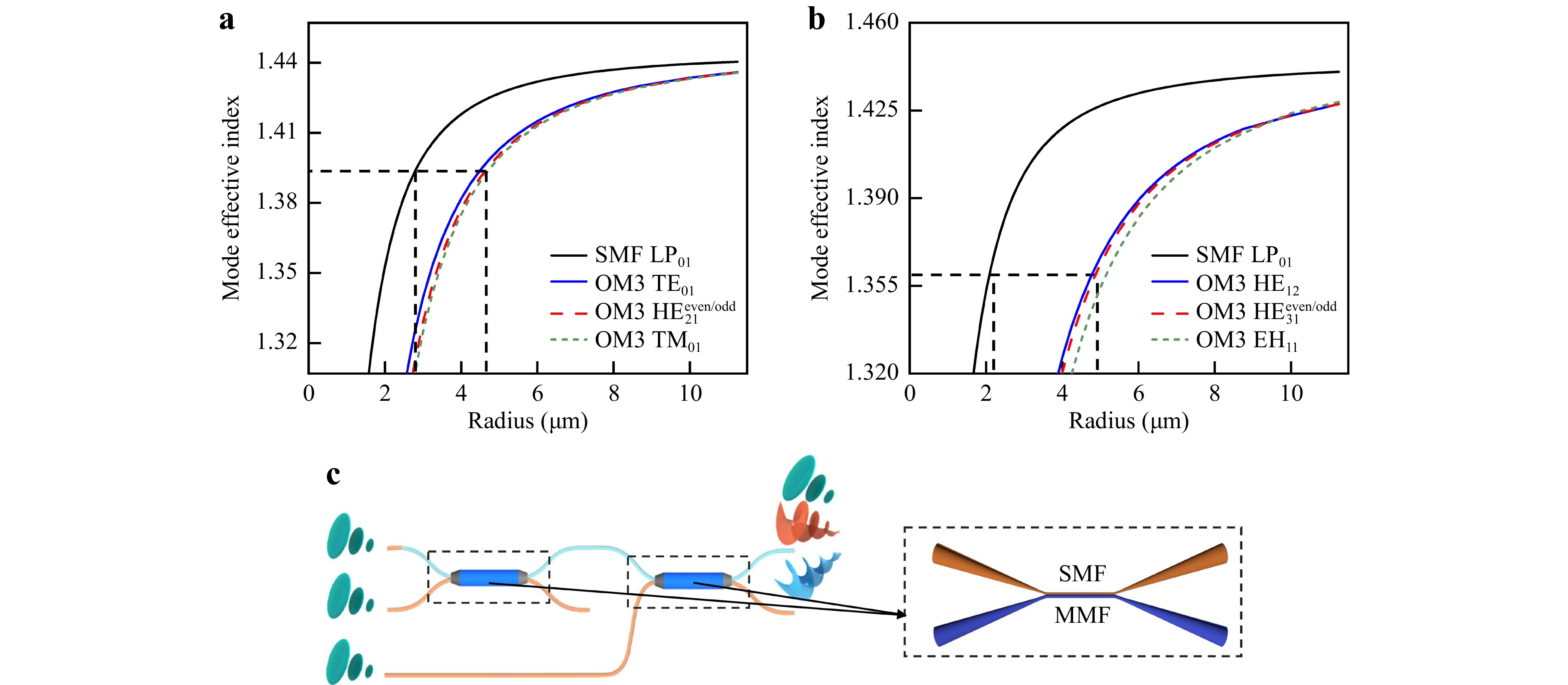
Fig. 3 a, b Simulated effective indices of different modes in SMF and OM3 as functions of the fibre cladding radius. c Schematic of the all-fibre OAM mode (de)multiplexer
The output end of the all-fibre OAM mode demultiplexer was connected to a single-mode array fibre and light was vertically coupled to the chip using gratings. Optical switching was performed through the photonic neural network chip, and subsequently, the light was vertically coupled out of the chip and into the single-mode fibre array. The all-fibre OAM mode multiplexer was then used to couple and multiplex the light into the multimode fibre carrying the multi-channel OAM modes. This achieves multi-channel OAM mode optical switching in multimode fibres. To control the switching state, we used a computer to control the multichannel power-supply system based on a microcontroller and adjusted the phase shifters on the chip. The parameters of the state matrix of the phase shifters were obtained through offline learning and called during real-time operations.
The entire system, from multimode fibre input to multimode fibre output, forms the “Fibre-Chip-Fibre” type OAM mode optical switching system. Fig. 4 shows the schematic of this system. During the experiment, the zeroth-, first-, and second-order OAM modes were loaded with quadrature phase-shift keying (QPSK), 8-ary quadrature amplitude modulation (8-QAM), and 16-ary quadrature amplitude modulation (16-QAM) signals, respectively, to verify the functionality of OAM mode optical switching. For instance, when the switching state of the silicon-based neural network chip was set to exchange input channels 1, 2, and 3 with output channels 2, 3, and 1, the 16-QAM, QPSK, and 8-QAM signals carried by the zeroth-, first-, and second-order OAM modes were swapped with the first-, second-, and zeroth-order OAM modes, respectively.
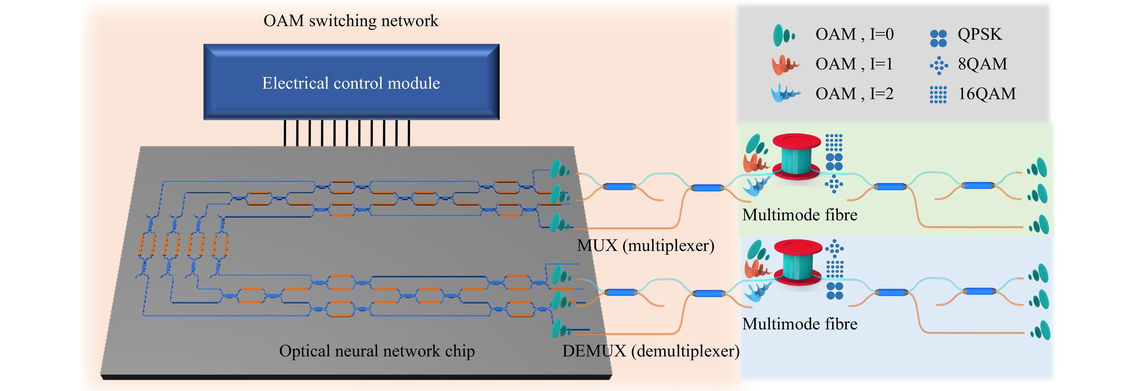
Fig. 4 Schematic of the fibre-chip-fibre OAM modes optical switching. DEMUX: Demultiplexer; MUX: Multiplexer.
-
To demonstrate the parameter optimisation of the silicon-based neural network chip and its application in multimode fibre OAM mode switching, the experimental setup shown in Fig. 5 was constructed. The setup was divided into four main parts: transmitter, receiver, mode-switching network, and learning device.
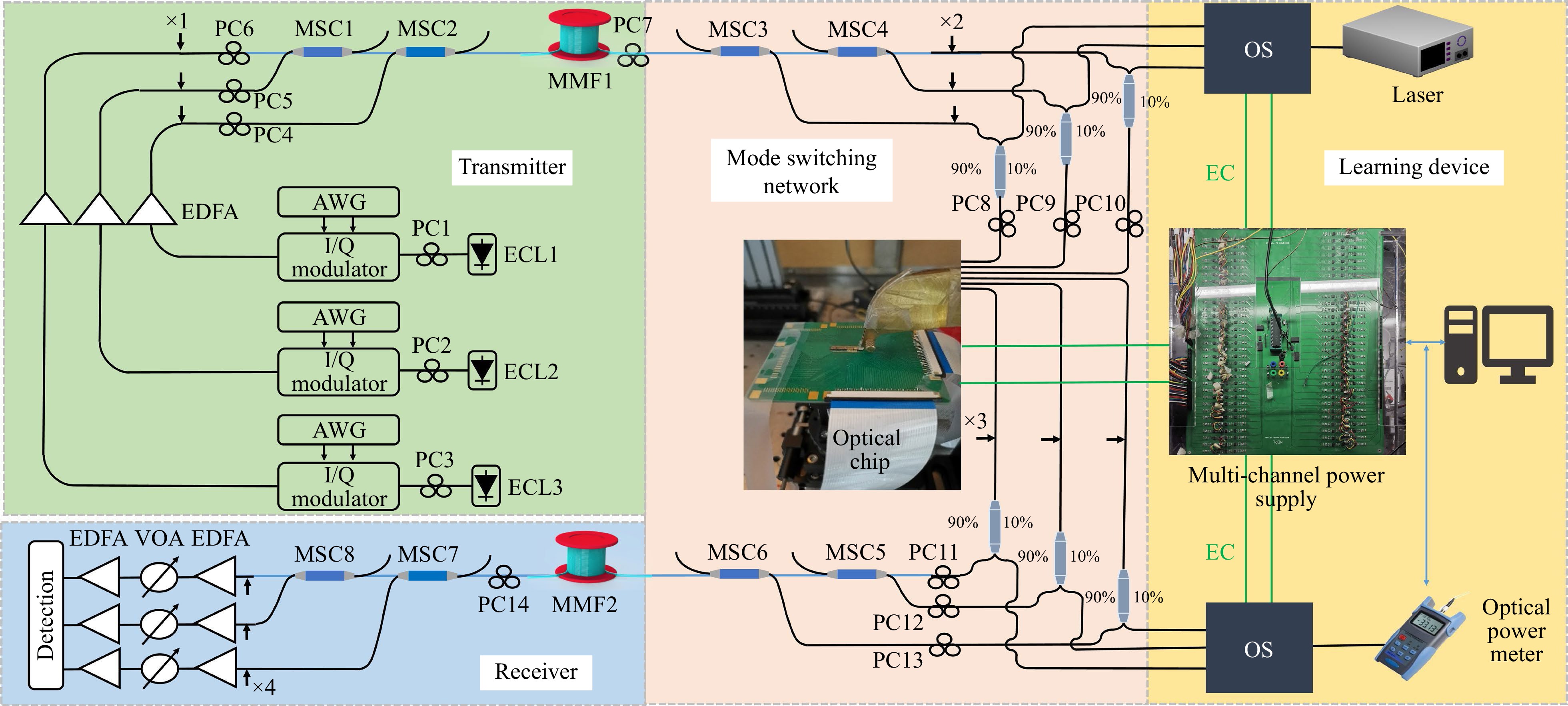
Fig. 5 Experimental setup diagram for multimode fibre OAM mode exchange using a silicon-based neural network chip. ECL: external cavity laser; PC: polarization controller; AWG: arbitrary waveform generator; I/Q Modulator: in-phase/quadrature modulator; EDFA: erbium-doped fibre amplifier; MSC: mode selective coupler; MMF: multimode fibre; VOA: variable optical attenuator; EC: electrical control; OS: optical switch.
At the transmitter, three external cavity lasers (ECLs) were employed as 1550 nm laser sources, which were then modulated by in-phase/quadrature (I/Q) modulators. Three high-order modulation format signals were produced using arbitrary waveform generators (AWGs) and loaded onto the I/Q modulators for laser modulation. Owing to the polarisation sensitivity of the I/Q modulators, polarisation controllers (PC1, PC2, and PC3) were used to adjust the polarisation states of the laser sources. After laser modulation, the three modulated optical signals were amplified by the erbium-doped fibre amplifiers to approximately 20 dBm and then fed into an all-fibre OAM mode multiplexer, where three OAM modes carrying different data information were multiplexed and transmitted through the multimode fibre. Polarisation controllers (PC4, PC5, and PC6) in the mode multiplexer assisted in optimising the polarisation state for enhanced OAM mode-multiplexing performance. After transmission through a 5-km multimode fibre OAM mode multiplexed optical communication link, three OAM modes carrying different data information became accessible at the multimode fibre interface.
At the receiver, a similar 5-km multimode fibre OAM mode multiplexed optical communication link was used, and the signals were subsequently demultiplexed by an all-fibre OAM mode demultiplexer into single-mode fibres for detection. The transmitter and receiver with 5-km multimode fibres can be perceived as two separate multimode fibre OAM mode multiplexed optical communication subnetworks. A silicon-based neural network chip was employed for OAM mode switching at the network connection node. The mode-switching network comprised an all-fibre OAM mode demultiplexer, a silicon-based neural network chip, and an all-fibre OAM mode multiplexer. As indicated by the labelled positions x1, x2, x3, and x4 in Fig. 5, signal collection and offline processing are performed at these locations to analyse the signal bit-error rate (BER) performance, which characterizes the multimode fibre OAM mode multiplexing and mode switching performance.
In the experiment, the grating vertical coupling input and output ports on the chip were positioned on one side of the chip during chip design to match the 16-port vertical coupling single-mode fibre array. Each input and output port utilised a TE vertical coupling grating with a standard spacing of 127 μm. At the input coupling end, polarisation controllers (PC8, PC9, and PC10) were used to adjust the polarisation of the input light to ensure an optimal TE polarisation for the vertical coupling grating. The developed silicon-based neural network chip was embedded in a predesigned printed circuit board adapter, where the chip pins were connected to those of the printed circuit board using wire bonding. Standard solder pads were formed through the printed circuit board, and a wire array was connected to the multichannel power-supply output in the learning device.
The learning device for the mode-switching network was assisted by six 90:10 single-mode fibre couplers. These couplers were divided into two groups, positioned before and after the chip input and output, respectively, corresponding to the three mode channels in each group. Because the coupling ratio of the couplers in the learning device used only 10% of the optical power, the optical communication system was minimally affected. In the learning device, a pair of lasers and power meters were used for the learning system to read the transmission coefficients from the input ports of the chip to its output ports. An optical switch was placed before the laser and after the power meter, to switch the couplers to read the corresponding transmission coefficients from the input to the output. The 3 × 3 transmission coefficient matrix U of the silicon-based neural network chip was obtained using three switches each at the laser output and power meter input. The multichannel power supply provided four power output ports for controlling the two optical switches, while an additional 36 ports were used to control the MZI array of the silicon-based MZI neural network chip. Finally, the computer controlled the aforementioned optical switches, power meters, and homemade power array, forming a feedback control loop.
The silicon-based neural network chip served as the core for the optical switching function in the fibre–chip–fibre OAM mode switching system. In this context, we adopted the aforementioned 4 × 4 MZI network architecture, which realised arbitrary 3 × 3 optical switching matrices. Initially, we validated the optical switching functionality of the silicon-based neural network photonic chip and stored well-trained configuration parameters for subsequent system experiments. We employed an improved gradient algorithm to train the chip, as shown in Fig. 6a. During the training process, the exchange matrix configuration was obtained by varying the voltages applied to each phase shifter. The training began with predefined parameters, including the learning rate η, target transmission matrix $ {U}_{aim} $, and initialisation of the applied voltage of each phase shifter. Throughout training, we defined the evaluation function as
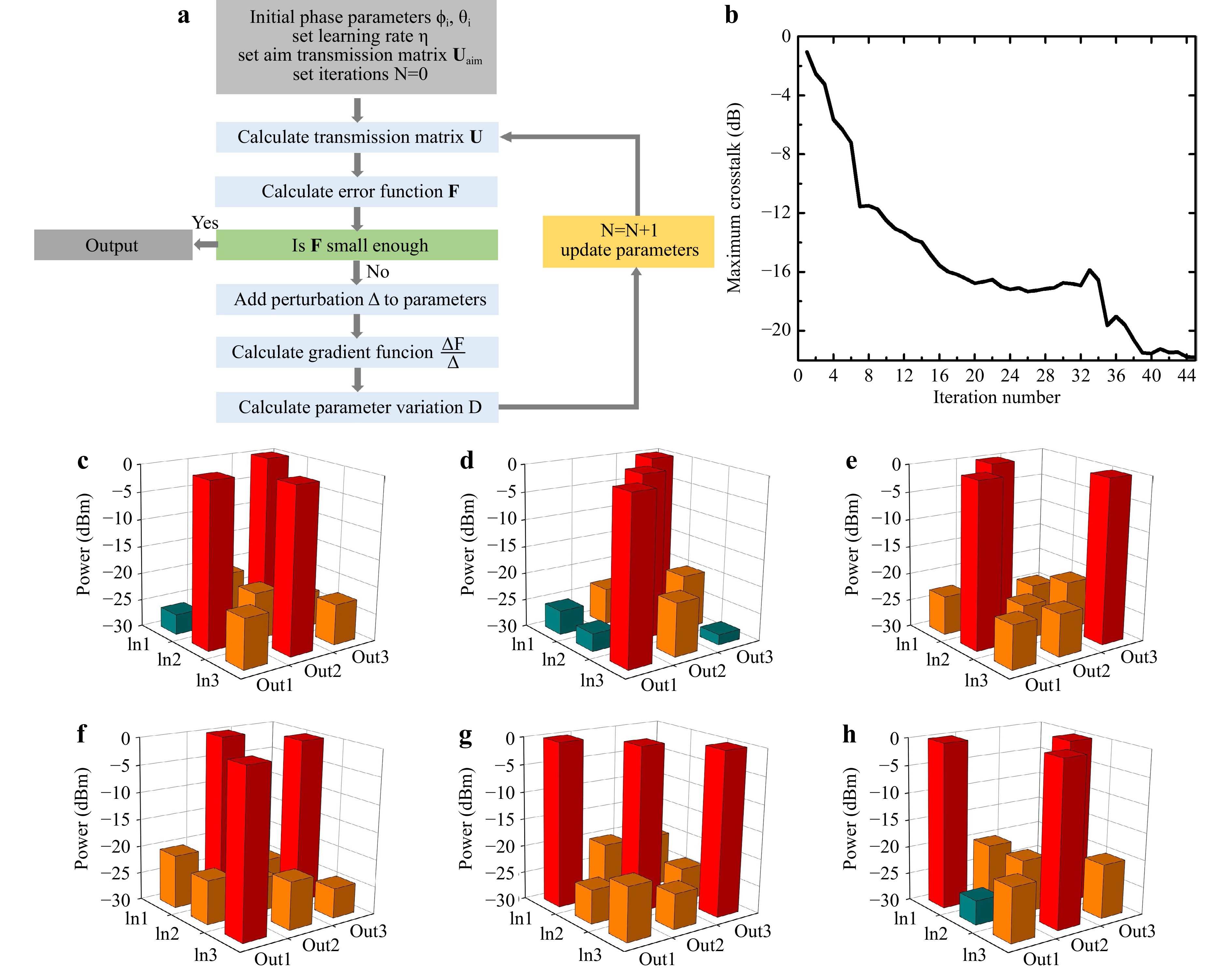
Fig. 6 a Flowchart of the gradient descent algorithm. b Curve showing the variation of the experimentally measured maximum crosstalk with optimization iteration cycles during the switch from channels 1, 2, and 3 to channels 2, 3, and 1. c–h Crosstalk matrices of the silicon-based neural network chip in six different switching states, where inputs from channels 1, 2, and 3 are exchanged to outputs: c channels 3, 1, 2; d channels 3, 2, 1; e channels 2, 1, 3; f channels 2, 3, 1; g channels 1, 2, 3; h channels 1, 3, 2.
$$ \mathrm{F}={|U-{U}_{aim}|}^{2} . $$ (3) The current transmission matrix U and current evaluation function F were calculated using power meter readings. Gradients were computed If the current evaluation function failed to satisfy the required level of low interference. By applying perturbations to each phase shifter, individual gradients $ {\boldsymbol{G}}_{\boldsymbol{j}}=(\boldsymbol{F}\left({\boldsymbol{a}}_{1},{\boldsymbol{a}}_{2},\cdot \cdot \cdot ,{\boldsymbol{a}}_{\boldsymbol{j}}+\boldsymbol{\Delta },\cdot \cdot \cdot ,{\boldsymbol{a}}_{\boldsymbol{M}}\right)- \boldsymbol{F}({\boldsymbol{a}}_{1},{\boldsymbol{a}}_{2},\cdot \cdot \cdot , {\boldsymbol{a}}_{\boldsymbol{j}},\cdot \cdot \cdot ,{\boldsymbol{a}}_{\boldsymbol{M}}))/{\boldsymbol{\Delta }} $ were determined. The parameter change quantity was calculated using the formula: $ D=-\eta F{G}_{j} $ and then applied to update the parameters of all the phase shifters.
In the actual experiment, we employed a uniform parameter representation, replacing φ and θ with a. The voltage parameters were set as follows:
$$ {V}_{i}=\frac{{V}_{min}+{V}_{max}}{2}+\frac{{V}_{max}-{V}_{min}}{2}\cdot sin\left({a}_{i}\right) . $$ (4) The specific training process is outlined below and a flowchart is shown in Fig. 6a.
1. Set algorithm initialisation parameters: Initialise phase parameters $ {\mathrm{a}}_{i} $, set a fixed learning rate η, determine the target transmission matrix $ {U}_{aim} $ based on application requirements, and set initial and maximum iteration rounds to terminate the algorithm if convergence is not achieved.
2. Control the power meter and optical switch to read the output power of the neural network chip under the current parameters and obtain the current transmission matrix U.
3. Substitute the measured U into the error evaluation function F and record the result. Evaluate the error function to determine whether the loop should be exited.
4. Apply a fixed perturbation voltage Δ to each current phase shifter state parameter. After each perturbation, re-measure U, calculate the new F, and record the result. Restore the parameters to their respective states before the perturbation. Compile all the new F values into a matrix (error matrix) divided by the corresponding perturbation amount to obtain the gradient matrix G. When there are many parameters, batch optimisation can be performed to reduce the computational load in each batch.
5. Substitute the gradient and error matrices into the parameter change formula $ \mathrm{D}=-\mathrm{\eta }\mathrm{F}G $, obtain the parameter change determined in this round of optimisation, update the parameters, and re-enter step 2.
This method confines the voltage within the ranges of $ {V}_{min} $ and $ {V}_{max} $, effectively preventing thermal resistance-related damage to the phase shifters. Fig. 6b illustrates the switching of channels 1, 2, and 3 to channels 2, 3, and 1, along with the curve depicting the maximum crosstalk variation during the parameter optimisation iterations. Certain points on the curve exhibit irregularities that can partly be attributed to power fluctuations in the experiment and the difficulties in precisely aligning $ {V}_{min} $ and $ {V}_{max} $ derived from the intermediate parameter “a” to achieve a full 4π phase shift. Under this switching configuration, a maximum crosstalk of less than -21 dB was achieved after more than 40 iterations. Fig 6c–h show the crosstalk matrices of the silicon-based neural network chip optical switching for six different switching configurations. The maximum crosstalk remains below –18.7 dB for all six configurations. The voltages for all phase shifters in each switching configuration were recorded and stored for subsequent experiments.
In the experiment, we performed separate tests for the intensity distribution pattern of the emitted modes at the transmitter and their interference patterns with a reference Gaussian beam to validate the excitation and multiplexed transmission of the zeroth-, first-, and second-order OAM modes in the multimode fibre. As shown in Fig. 7a, the zeroth-order OAM mode is circular with a bright spot at the beam centre, whereas the first- and second-order spots are annular rings with null intensity at the beam centre. This observation verifies that the intensity distributions are consistent with their respective mode characteristics. To further investigate the phase distribution, we established a reference Gaussian beam-splitting coaxial interferometer and tested the interference patterns with the reference Gaussian beam, as illustrated in the interference patterns of Fig. 7a. The interference pattern for the zeroth-order mode resembles “Newton’s rings”, which is transformed into a “swallowtail” pattern under slight fibre disturbance. The first- and second-order modes exhibit one and two helical interference patterns, respectively. The comprehensive characterisation of the distribution of these interference patterns confirmed that the phase distributions of the modes corresponded to their expected patterns. Considering both the intensity and phase distributions of the modes, it is evident that the multiplexed transmission in the multimode fibre encompasses the zeroth-, first-, and second-order OAM modes. Similarly, the intensity distribution patterns and interference patterns of the receiver modes after transmission through a 5-km multimode fibre are presented in Fig. 7b. The experimental results indicate that after mode switching, the multimode fibre effectively multiplexes and transmits zeroth-, first-, and second-order OAM modes.
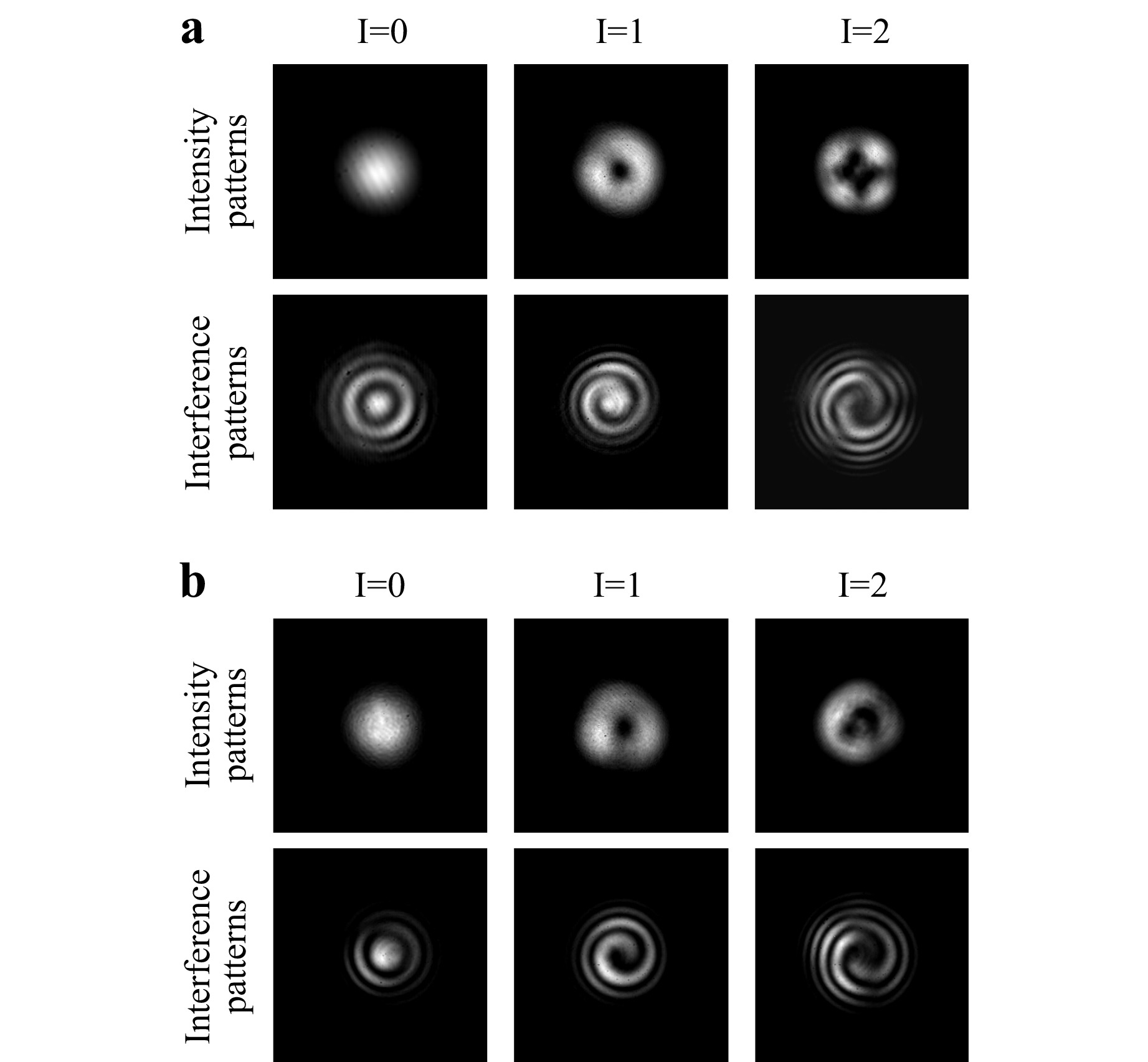
Fig. 7 Intensity distribution and interference patterns of zeroth-, first-, and second-order OAM modes after multimode fibre transmission. a Transmitter after 5-km multimode fibre transmission; b Receiver after 5-km multimode fibre transmission.
After confirming the functionality of the silicon-based neural network chip and all-fibre mode demultiplexer, we systematically validated the fibre–chip–fibre-type OAM mode optical switching system. For swapping input channels 1, 2, and 3 with output channels 2, 3, and 1, we loaded the optimised configuration parameters onto the chip. Simultaneously, we activated three ECLs, loading QPSK, 8-QAM, and 16-QAM signals, to perform multimode fibre OAM mode multiplexed transmission and OAM mode optical switching. Fig. 8a depicts the BER variation with the received signal-to-noise ratio (OSNR) at system positions x1, x2, x3, and x4. Here, x1 represents the back-to-back test position; x2 denotes the position after 5-km of multimode fibre multiplexed transmission and passage through the demultiplexer; x3 indicates the position after the chip output; and x4 represents the position after mode swapping and further 5-km of multimode fibre multiplexed transmission and demultiplexing. The red line in the figure denotes the threshold of 20% hard-decision forward error correction (20% HD-FEC). The signal transmission can be error-corrected using 20% HD-FEC only when the BER falls below this threshold, thereby ensuring an error-free transmission. The back-to-back BER curve at the 20% HD-FEC threshold has a received OSNR of approximately 20.4 dB at x1 and around 22 dB at x2, indicating an introduced OSNR penalty of 1.6 dB at x2. This is partly because of channel crosstalk introduced by the pre-multiplexing demultiplexer of the chip and partly because of intermodal crosstalk introduced by 5-km of multimode fibre multiplexed transmission. Although the intermodal crosstalk in multimode fibres was relatively small, the substantial refractive-index differences between the modes in the fibre resulted in signal loss. The channel crosstalk was further reduced by improving the multiplexing demultiplexer. At position x3, the received OSNR at the 20% HD-FEC threshold was approximately 23.8 dB, indicating an introduced OSNR penalty of approximately 1.8 dB from x2 to x3. This is the combined result of channel crosstalk introduced by optical chip switching and internal chip loss. At position x4, an OSNR penalty of approximately 3.2 dB was introduced. This was attributed to the channel crosstalk introduced by the post-multiplexing demultiplexer of the chip and the reduction in signal power, which places the receiving-end EDFA outside its optimal input power range. We collected signals at approximately equal OSNR levels from these four positions. Their constellation diagrams are presented in the inset of Fig. 8a−c illustrate the BER variation with the OSNR for the 8-QAM and 16-QAM signals when input channels 1, 2, and 3 are swapped for output channels 2, 3, and 1 at different positions within the system. These trends are highly similar to those presented in Fig. 8a for the QPSK signals. The overall OSNR penalties for the 8-QAM and 16-QAM systems are approximately 5.8 dB and 5.9 dB, respectively, with chip-induced OSNR penalties of 1.6 dB and 2.1 dB, respectively. At the 20% HD-FEC threshold, the received OSNR for the back-to-back 8-QAM BER curve was approximately 22 dB, whereas that for 16-QAM was approximately 23.3 dB. This difference occurs because a higher modulation order of 16-QAM requires a higher OSNR. The OSNR penalties for the 8-QAM and 16-QAM signals at different positions were comparable, indicating a relatively balanced degradation of the different modulation format signals during system transmission. This observation was further supported by the constellation diagrams.
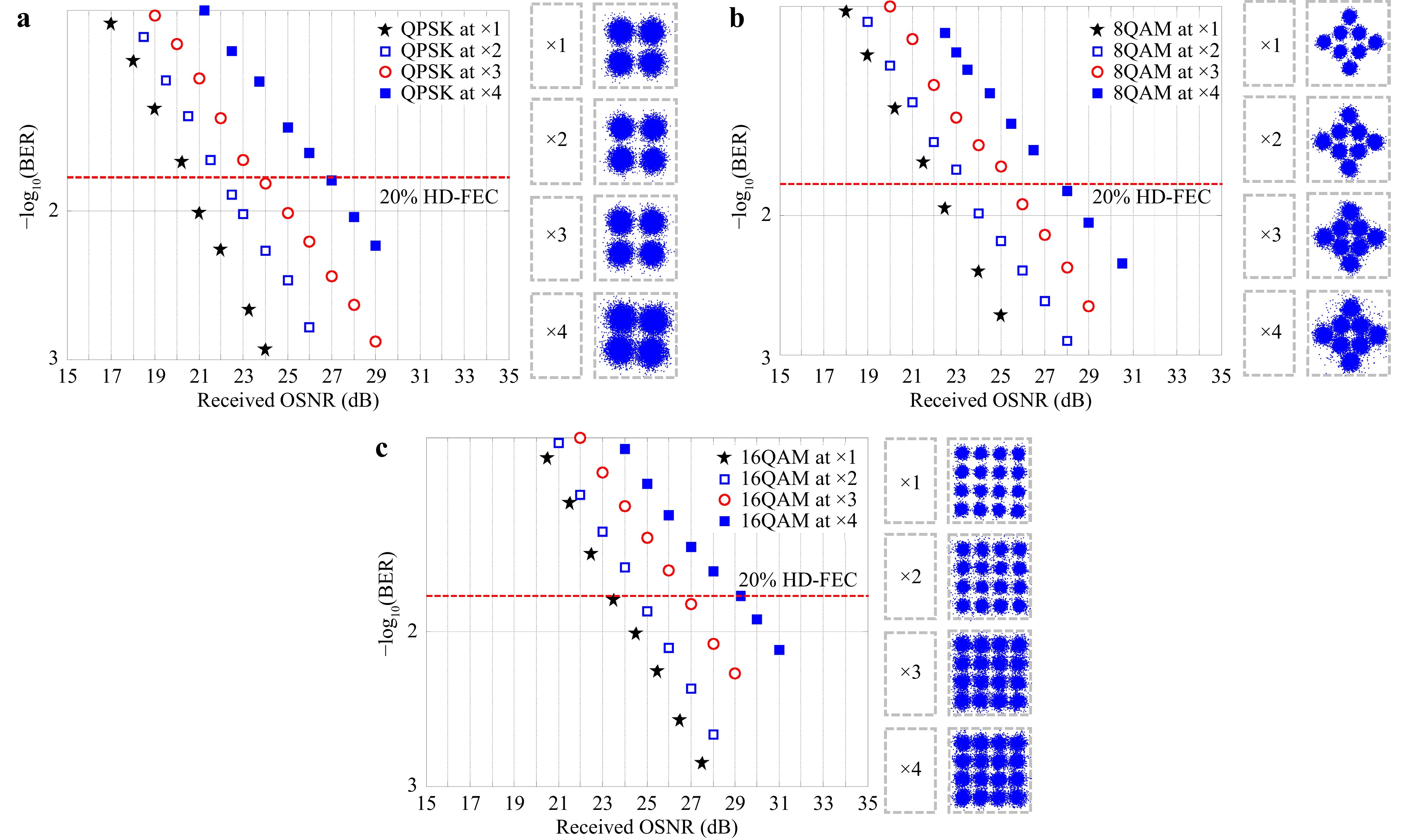
Fig. 8 BER versus OSNR curves and constellation diagrams of different signals at four positions in the system under multimode fibre OAM mode multiplexing: a QPSK; b 8-QAM; c 16-QAM.
To provide a clear comparison of the signal degradation introduced by the mode-channel crosstalk during mode multiplexing, Fig. 9a presents the BER variation with the OSNR for QPSK, 8-QAM, and 16-QAM signals at position x4 under both three-channel multiplexing and single-channel transmission scenarios. For single-channel transmission, the OSNR penalties for QPSK, 8-QAM, and 16-QAM signals are reduced by 4.6 dB, 4.3 dB, and 4.7 dB, respectively. This portion of the OSNR penalty arises from mode channel crosstalk during the mode-multiplexing process. The figure also presents constellation diagrams of the different mode channels at various positions under OAM mode multiplexing. A comparison of the x1 and x2 positions before chip switching with the x3 and x4 positions after chip switching demonstrates that OAM mode optical switching corresponding to the input-output channel configurations of 1, 2, 3 to 2, 3, 1 carrying different data information is achieved. Further analyses were conducted on crosstalk introduced at different positions within the experimental system. At positions x2, x3, and x4, ECL1, ECL2, and ECL3 were successively activated to measure the outputs of the three channels at different positions, and the crosstalk matrix was obtained as shown in Fig. 9b–d. The maximum crosstalk at x2 is approximately -16 dB, while crosstalk introduced at x3 exhibits negligible degradation. At x4, the crosstalk increases to around −13 dB. These results demonstrate that the crosstalk is primarily introduced by the imperfections in the all-fibre mode demultiplexer.
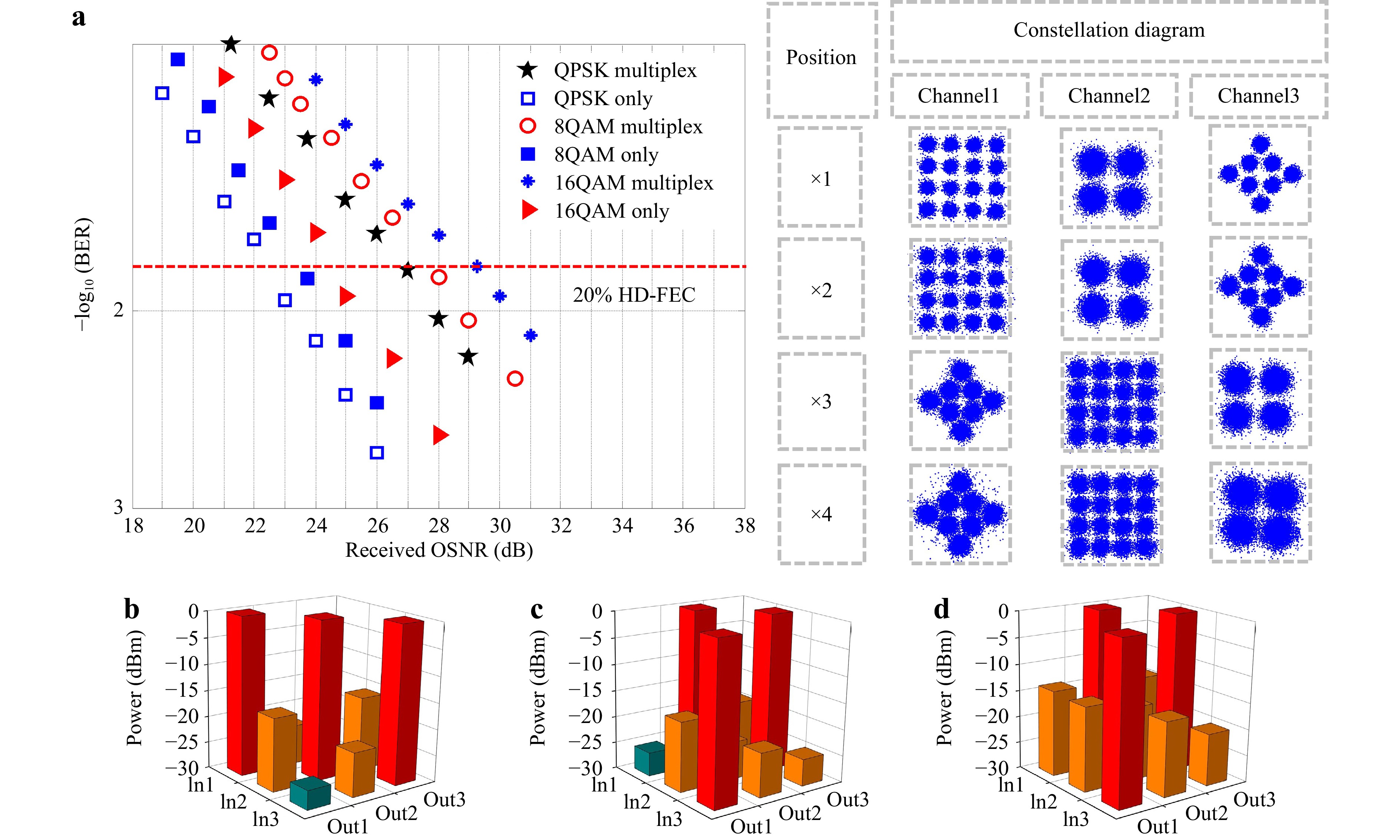
Fig. 9 a BER versus OSNR curves of QPSK, 8-QAM, and 16-QAM signals at position x4 under three-channel multiplexing and single-channel transmission conditions, along with constellation diagrams of different channels at different positions under three-channel multiplexing. Crosstalk matrix of mode switching at positions b x2, c x3, and d x4.
Fig. 10 shows the BER variation with the OSNR for the three advanced modulation formats under different switching configurations. For both switching states at position x4, the OSNR penalty for the QPSK, 8-QAM, and 16-QAM signals was less than 0.2 dB. The right-hand figure presents the constellation diagrams for the two switching configurations in channels 1, 2, and 3, indicating the successful implementation of distinct switching. For comparison, the figure on the right also presents constellation diagrams for the single-channel scenario without an exchange.
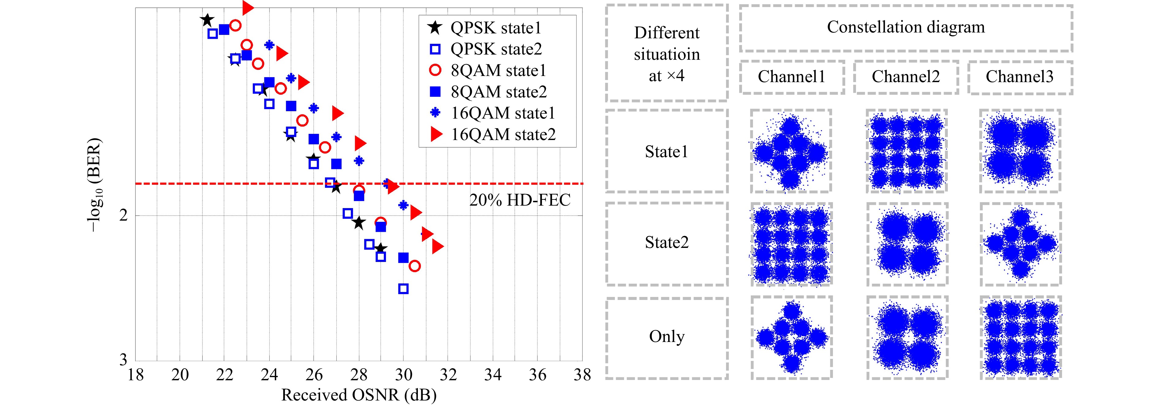
Fig. 10 BER versus OSNR curves of QPSK, 8-QAM, and 16-QAM signals at position x4 under two different switching states, along with constellation diagrams at position x4 for switching state 1, switching state 2, and single-channel transmission. (Switching state 1: Input channels 1, 2 and 3 swapped to output channels 2, 3 and 1. Switching state 2: Input channels 1, 2 and 3 swapped to output channels 1, 2 and 3.)
-
In summary, all-fibre OAM mode (de)multiplexers and a silicon-based neural network chip were fabricated and combined to validate a multimode fibre OAM mode optical switching system. To demonstrate the capabilities of the optical neural network chip, an improved gradient algorithm was used for switching configuration training, achieving comprehensive training for all 3 × 3 optical switching matrices with a maximum inter-channel crosstalk below −18.7 dB. Simultaneously, within the context of multimode fibre OAM mode multiplexing communication, three distinct OAM modes were harnessed to transmit diverse high-order modulation format signals (QPSK, 8-QAM, and 16-QAM). This experimental approach effectively verified the performance of the data-carrying multimode fibre OAM mode optical switching. A BER performance assessment conducted for different system positions under various OSNR conditions and analyses of constellation diagrams under consistent OSNR levels demonstrated that higher-order modulation formats entailed more stringent OSNR prerequisites. In addition, the resilience of different modulation format signals to impairments was relatively balanced, with crosstalk primarily originating from the components within the all-fibre OAM mode (de)multiplexers. The proposed optical mode-switching system, which was based on an optical neural network chip, exhibited excellent performance in optical communication experiments. The matrix scale of this neural network chip can be expanded to any N × N network, thereby demonstrating strong scalability. We incorporated mainstream optimisation algorithms such as the improved gradient descent algorithm proposed in this study to achieve on-chip high-performance training with adaptive configuration capabilities. In addition to using the OAM modes as the optical exchange mode in this solution, different mode (de)multiplexers can be combined to achieve multimode optical exchange in other mode bases. This combination provides a flexible and high-performance solution for multimode optical exchange.
-
This work was supported by the National Natural Science Foundation of China (NSFC) (62125503, 62261160388), Natural Science Foundation of Hubei Province of China (2023AFA028), Key R&D Program of Hubei Province of China (2020BAB001, 2021BAA024), and Innovation Project of Optics Valley Laboratory (OVL2021BG004).
Flexible orbital angular momentum mode switching in multimode fibre using an optical neural network chip
- Light: Advanced Manufacturing 5, Article number: (2024)
- Received: 18 September 2023
- Revised: 29 March 2024
- Accepted: 07 April 2024 Published online: 12 July 2024
doi: https://doi.org/10.37188/lam.2024.023
Abstract: Mode-division multiplexing technology has been proposed as a crucial technique for enhancing communication capacity and alleviating growing communication demands. Optical switching, which is an essential component of optical communication systems, enables information exchange between channels. However, existing optical switching solutions are inadequate for addressing flexible information exchange among the mode channels. In this study, we introduced a flexible mode switching system in a multimode fibre based on an optical neural network chip. This system utilised the flexibility of on-chip optical neural networks along with an all-fibre orbital angular momentum (OAM) mode multiplexer-demultiplexer to achieve mode switching among the three OAM modes within a multimode fibre. The system adopted an improved gradient descent algorithm to achieve training for arbitrary 3 × 3 exchange matrices and ensured maximum crosstalk of less than −18.7 dB, thus enabling arbitrary inter-mode channel information exchange. The proposed optical-neural-network-based mode-switching system was experimentally validated by successfully transmitting different modulation formats across various modes. This innovative solution holds promise for providing effective optical switching in practical multimode communication networks.
Rights and permissions
Open Access This article is licensed under a Creative Commons Attribution 4.0 International License, which permits use, sharing, adaptation, distribution and reproduction in any medium or format, as long as you give appropriate credit to the original author(s) and the source, provide a link to the Creative Commons license, and indicate if changes were made. The images or other third party material in this article are included in the article′s Creative Commons license, unless indicated otherwise in a credit line to the material. If material is not included in the article′s Creative Commons license and your intended use is not permitted by statutory regulation or exceeds the permitted use, you will need to obtain permission directly from the copyright holder. To view a copy of this license, visit http://creativecommons.org/licenses/by/4.0/.

 DownLoad: