


-
Three-dimensional (3D) laser writing inside narrow-bandgap semiconductors, including crystalline silicon (c-Si), is a topic attracting today particular attention. This holds a clear potential to complement lithographic planar methods for the manufacturing of ultra-high-density semiconductor devices. Experiments show that ultrashort pulses in the near-infrared or mid-infrared domains focused in small spots can lead to localized energy deposition by nonlinear absorption anywhere in the 3D space of any semiconductor material1,2. However, the strong propagation nonlinearities and plasma effects make it extremely difficult to deliver enough energy densities for the writing of permanent modifications in most cases3,4. There are several solutions recently identified to this problem1. The first is the use of experimental configurations to perform interactions with an energy flux based on more angular components than conventional laser processing methods. This was evidenced by a proof-of-concept experiment leading to the first modifications inside c-Si with sub-100-fs pulses while applying the solid-immersion focusing technique to work with a numerical aperture (NA) largely exceeding the unity5. The second is to deviate from the femtosecond regime and introduce longer irradiation components to lower the peak power of the processing beams. This strategy can rely on the use of ultrashort pulses exhibiting a limited contrast6, THz burst mode irradiation approaches7,8, and/or the direct use of picosecond9,10 or nanosecond pulses11-14. These approaches have been studied and exploited during the last years to make important technological demonstrations including the direct writing of waveguides14-16 and other optical functionalities13,17,18, stealth dicing8,11,12, transmission laser welding19,20, and the fabrication of various 3D structures by laser-assisted etching methods13,21.
Following these recent successes, there is today a timeliness to introduce beam-shaping strategies to further optimize the interactions in semiconductors and provide the same degree of freedom as the one exploited in other 3D writing technologies22,23. For instance, after the first feasibility demonstrations of waveguide writing14,15, Wang et al. and others implemented the conventional slit beam-shaping method to produce focus distributions with circular cross-sections so that transverse writing of symmetric waveguides become accessible inside Si16,24. More recently, Tokel et al. interestingly demonstrated sub-surface 2D-confined nanochannel generation in c-Si by scanning micro-Bessel nanosecond laser beams at the vicinity of preformed structures25. While the nature of this pre-structure non-local seeding technique is associated with freedom limitations for 3D manufacturing applications, this represents an important advancement as it tends to translate in the bulk an important concept for nanoscale writing resolutions and exploited on surfaces26.
It is worth noting this is not the first attempt to exploit Bessel beams in the context of bulk Si studies. Some previous works studied the processing performances of micro-Bessel beams produced in the infrared domain27-29 and configurations similar to those exploited for fabricating high-aspect-ratio nanochannels in glasses using single femtosecond pulses at a wavelength of 800 nm30. High-aspect-ratio drilling in Si with performances similar to those demonstrated in dielectrics would be highly desirable. It would offer an attractive alternative to currently applied reactive ion etching solutions (e.g. Bosh process) for through-silicon-via (TSV) formation, which are needed for interconnections in modern multilayer 3D microelectronics. However, all these attempts as well as ours in the present paper could only confirm important physical limitations to using ultrashort pulses. The technological demonstration of TSV formation by tailored infrared Bessel beams remains limited to ultrathin Si wafers (~100 μm) with holes produced by percussion drilling and an aspect ratio hardly exceeding 5, posing questions on the real benefit of the use of infrared wavelengths29.
In this article, we revisit the question of the possible formation of ultra-high-aspect-ratio structures in c-Si with Bessel beams. Capitalizing on recent advances in understanding the limitations of bulk-Si processing, we implement a configuration optimized to deliver the highest achievable intensities along channels through c-Si wafers. For optimization in the spatial domain, the previously mentioned work is encouraging to produce Bessel beams with extremely high angular components5. This leads us to propose and study a method based on axicon-lens doublets for beam-shaping. We show an approach that compares very well with usually applied image-relay methods28,31, with the advantage of simplicity to produce extremely high-angle beams. Although this is not a new method32-34, to the best of our knowledge, it is considered here for the first time in the context of laser processing. For optimized conditions in the time domain, we refer to recent reports on the pulse-duration dependence of the problem35, and systematically compare the responses of the material to the applied femtosecond and stretched picosecond pulses. Some comparisons were also made in the nanosecond regime to confirm an optimum trade-off between nonlinear delocalization effects and efficient energy coupling with the material in the picosecond regime.
After discussing the features of the accessible beam focus conditions with the combinations of objective lenses and small-angle axicons perturbing the wavefront of tightly focused beams, we apply in c-Si a pseudo-Bessel beam exhibiting a sub-diffraction limited spot size of ~1.5 μm over an extended depth-of-focus largely exceeding 0.7 mm in free-space. Interestingly, using picosecond pulses we show how this allows the production of high-aspect-ratio optical TSV structures featuring a positive refractive index variation with respect to the pristine region. Contrasting with many previous studies, the modifications initiate in all cases from a modification created at the wafer surface which uniformly grows and self-propagates in the direction of the laser beam inside the sample on a pulse-to-pulse basis. The subsequent elongated structures obtained along the optical axis are thus obtained without any beam displacement. Using this approach, we demonstrate near 1-mm long plasmas and permanent microchannel modifications deep inside c-Si. We discuss time- and space-resolved observations contributing to a better understanding of the phenomena, and further extrapolate technological consequences given potentially new optically switchable TSV vertical interconnection technologies for multilayer Si-photonics and microelectronics systems.
-
Axicon is known to be one of the most convenient optical means for the generation of Bessel beams36-38. However, achieving high-angle conical Bessel beams is very crucial for material processing applications22. The conventional methods use image-relayed beams with a telescopic system for demagnification. However, this approach takes up working space, is sensitive to alignment imperfections, and remains always limited by the entrance pupil diameter and damage threshold of the last optical element28,31. In this section, we numerically investigate an alternative simple approach aiming at the generation of good-quality infrared Bessel-like beams. The approach involves a controlled perturbation of the spherical wavefront produced by an ideal focusing lens. It is based on combining a lens with a modest angle axicon so that a linear radial-dependence phase contribution is added to the quadratic phase associated with the lens. The ray diagram of such optical configuration is schematically depicted in Fig. 1a. Ray-tracing shows that the combination of an axicon and a lens as a doublet (i.e. axicon-lens doublet) has the ability to efficiently produce high-angle pseudo-Bessel beams with extended-depth-of-focus. In the case of a modest angle axicon (small perturbation), we expect the typical converging angle to be imposed by the focusing power of the lens and the obtained profile can be seen as an aberrated focus. We desire a Bessel-like elongated focus resulting from the angular components not all collapsing at the same distance, and an axial intensity distribution exhibiting a slowly varying leading edge before a sharp fall on its trailing edge. Moreover, ray-tracing of Fig. 1a directly showcases the relative focal shift in the pre-focal region in comparison to single-lens focusing. This corresponds to a situation where the converging angle of the beam components even exceeded the maximum half-angle that would be derived from the NA value of the focusing lens.
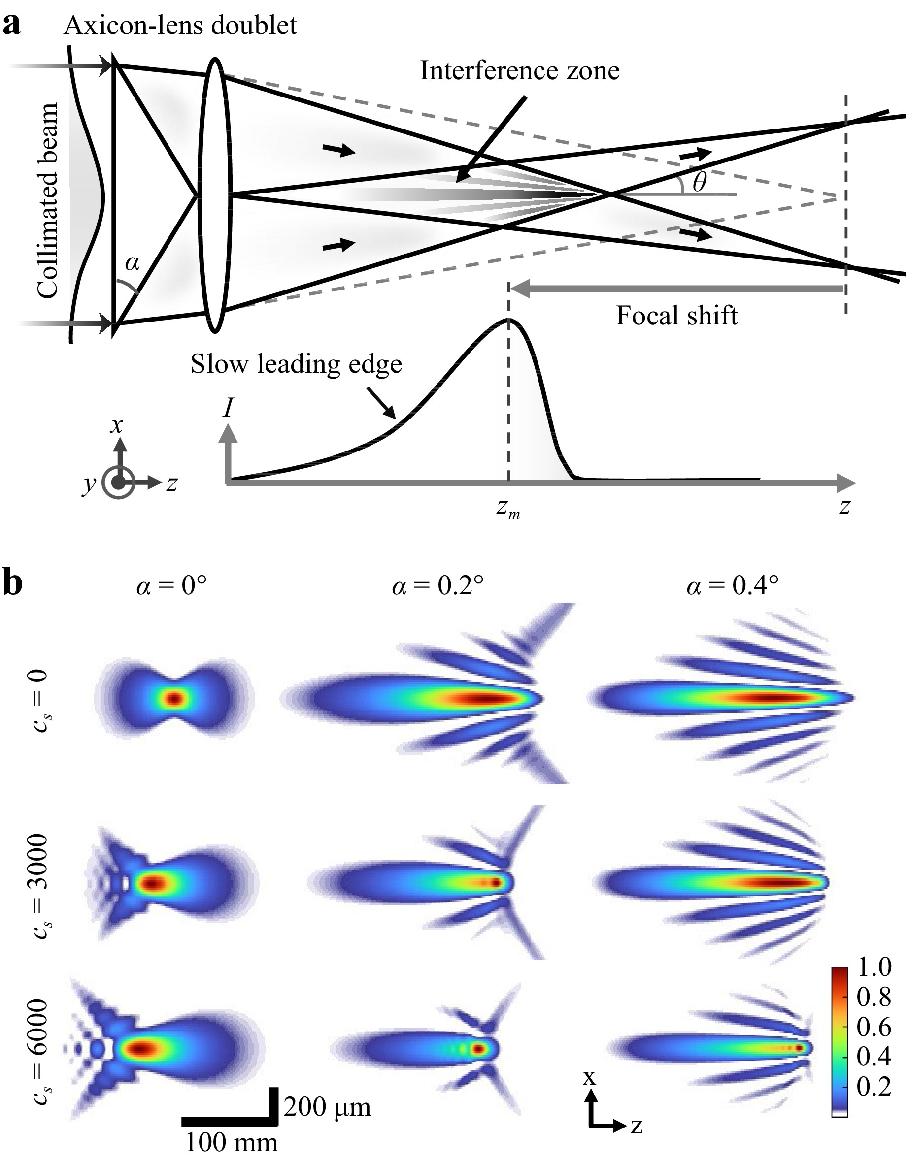
Fig. 1 a Schematic ray diagram for a Gaussian beam focused by an axicon-lens doublet resulting in a pseudo-Bessel beam. b Cross-sectional view of intensity distributions across the optical axis for beams calculated with different phase perturbation conditions. The beams are focused with axicon-lens doublets including a lens of 400 mm focal length. The parameters $ \alpha $ and $ c_{s} $ are the base angle of the axicon and spherical aberration strength, respectively.
To confirm the general characteristics of the pseudo-Bessel beams originating from the axicon-lens doublets, we perform propagation calculations. We simulate the propagation of beams with the consideration of an initial phase described by:
$$ \begin{array}{*{20}{l}} \Phi(r) = k \Bigg[\dfrac{r^2}{2f} + c_{s} \dfrac{r^4}{8f^3} + \alpha (n-1) r \Bigg] \end{array} $$ (1) where $ k $ is the free-space propagation constant, r is the space coordinate of the studied problem exhibiting a cylindrical symmetry, and $ \alpha $ is the base angle of the axicon with refractive index $ n $. The first term in Eq. 1 represents the quadratic phase for an ideal focusing lens with focal length $ f $. The second and third terms correspond to added phase perturbations to describe the studied situations. The second term is added for encountering potential spherical aberrations in practical situations. The latter is introduced by accounting for the second term of a Tailor series expansion of the spherical wavefront curvature (i.e. w(r) = [r2/2R + r4/8R3 +...]; R being the radius of the spherical wavefront) with strength arbitrarily defined by the parameter $ c_{s} $. The third term describes the effect of the addition of a thin axicon.
The simulations are performed based on a numerical model using the Fresnel transfer function method as described in references39,40. For valid calculations under the paraxial approximation, we consider here an input collimated Gaussian beam of beam-waist $ \omega_{0}=2.4 $ mm and wavelength $ \lambda $ = 1550 nm illuminating the axicon-lens doublet (at $ z $ = 0) including a lens with focal length $ f=400 $ mm. For varying levels of phase perturbations corresponding to different axicon-lens combinations, we numerically calculate the normalized longitudinal intensity maps ($ x $–$ z $ view) of the resulting beams in air along the propagation direction ($ z $), as shown in Fig. 1b. For a specific value of $ \alpha $, we calculate the beam intensity distributions by introducing different strengths of spherical aberration using the parameter $ c_{s} $. The values of $ c_{s} $ are arbitrarily set so that the beam focus is significantly affected, as it is commonly observed for bulk interaction in Si due to the high refractive index (~3.5) of the material causing strong refraction at the air-material interface. In this way, we can test the robustness of the produced beams to the spherical aberration level that will depend on the processing depth.
While the value $ \alpha $ = 0° represents the normal Gaussian focus distributions (first column of Fig. 1b), $ \alpha $ = 0.2° and 0.4° represent the formation of pseudo-Bessel focus distributions. For these two cases, the simulations reproduce the essential features expected from the ray-tracing configuration in Fig. 1a, that is, an elongated depth-of-focus with a slow leading edge followed by a sharp drop of intensity. In particular, the simulations confirm that a modest change in the spherical phase (visualized in Fig. S1 of the Supplementary Information) can significantly elongate the beam focus longitudinally without affecting the lateral resolution. With the calculated beam profiles exhibiting lobes, the numerical study emphasizes the relevance of the analogy made with Bessel beams. Fig. 1b shows the effectiveness of axicon-lens doublets as focusing elements to produce Bessel-like beams and also reveals the relative robustness of the produced features despite some spherical aberration levels inevitably occurring for the considered practical cases.
-
Based on our numerical observation, we now implement the beam-shaping strategy to generate high-angle pseudo-Bessel beams, as schematically depicted in Fig. 2a. In practice, we first concentrate on an axicon-lens doublet comprising an axicon with $ \alpha $ = 2° and a microscope objective lens of 0.45 NA equipped with a correction collar (c.c.) to compensate for spherical aberrations in Si. The two elements are placed in close proximity to each other (axicon in contact with the entrance pupil of the objective) and mounted on a motorized stage allowing its translation along the optical axis ($ z $). The doublet is then illuminated by a collimated picosecond laser beam having a beam-waist (radius at 1/e2) of 2.4 mm and so underfilling the objective entrance pupil of ~4.5 mm radius. The generated free-space beam distributions after the axicon-lens doublet are reconstructed by scanning the doublet configuration along the $ z $ axis with a precision of 20 μm through the imaging plane of a microscopy system (more details are given in the Experimental setup section), and hence recording the consecutive transverse beam profiles on an InGaAs array sensor. For a systematic comparison, we have also reconstructed the Gaussian focus distribution in free space with a precision of 1 μm by removing the axicon from the optical path. During these reconstruction processes in air, the spherical aberration c.c. value of the objective lens is always set to zero to avoid any undesired beam distortions.
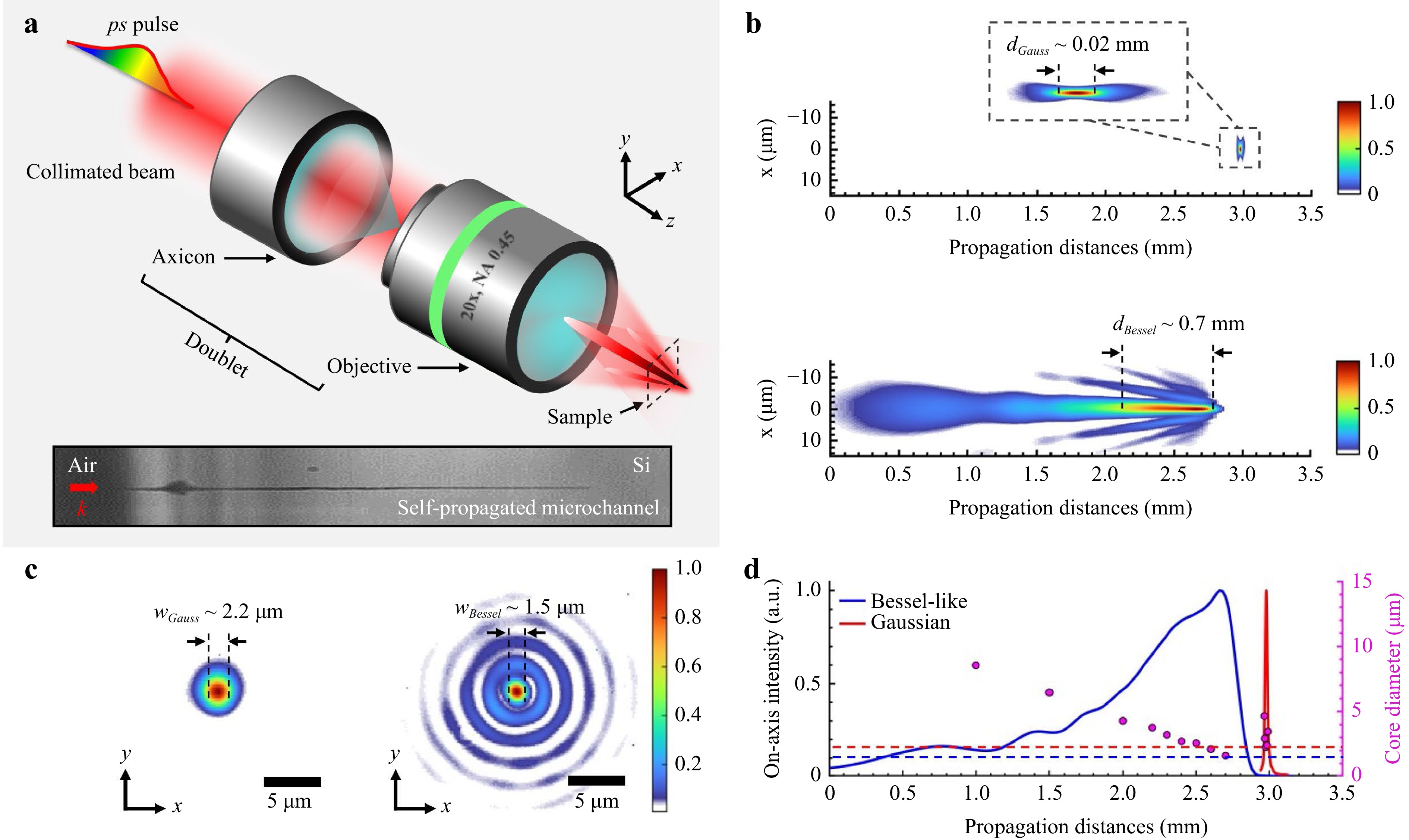
Fig. 2 a Schematic illustration of the beam-shaping scheme using the axicon-lens doublet to produce a high-angle pseudo-Bessel micro-beam. Inset: a typical high-aspect-ratio microchannel modification fabricated inside c-Si using repeated irradiations of picosecond pulses. $ k $ shows the laser propagation direction. b Measured longitudinal intensity maps ($ x $–$ z $ plane) of the Gaussian and pseudo-Bessel beams, respectively. Inset: zoomed view of the Gaussian focus distribution. c Images of the measured transverse beam profiles for the Gaussian and pseudo-Bessel beams at the peak on-axis intensity positions. The spot sizes are calculated at FWHM. d Normalized on-axis intensity distributions, and variation of the spot sizes along the propagation direction for the Gaussian and pseudo-Bessel beams, respectively. The dashed lines indicate the minimum spot sizes of the beams at the locations corresponding to the peak intensity.
The longitudinal intensity maps ($ x $–$ z $ plane) of the reconstructed beams are shown in Fig. 2b. It is observed that with these tight focusing conditions, which cannot be rigorously calculated with our numerical model, the axicon-lens doublet still efficiently produces a Bessel-like beam with an elongated depth-of-focus of $ d_{Bessel} \; \sim $ 0.7 mm (full width at half maximum, FWHM) to be compared to the Gaussian focus distribution with $ d_{Gauss} \; \sim $ 0.02 mm. The transverse profile images of the reconstructed beams at the peak on-axis intensity positions are shown in Fig. 2c. Remarkably, for the same input beam size the Bessel-like beam features a central core of sub-diffraction limited spot size ($ \omega_{Bessel} $) of ~1.5 μm (FWHM) surrounded by concentric circular rings, which is smaller than the ~2.2 μm spot size ($ \omega_{Gauss} $) measured for the Gaussian focus.
Fig. 2d represents the normalized on-axis intensity distributions of the measured beams. We observe a pre-focal shift of the peak intensity position (~0.3 mm) when the axicon is added. Notably, in contrast to a conventional Bessel beam, our spatially shaped Bessel-like beam features a gradually rising leading edge followed by a sharp drop of intensity along the optical axis. This can be seen as a degraded feature in comparison to other methods usually aiming at producing uniform intensity filaments. However, as we will see later, such distinct intensity distribution can actually be beneficial for precompensating nonlinear delocalization and losses scaling with processing depths, as identified in laser processing studies of Si1.
Furthermore, to assess the non-diffractive nature of the produced Bessel-like beam, we also show in Fig. 2d the variation of the measured spot sizes (FWHM) as a function of the propagation distance. As anticipated, the core size of the Bessel-like beam gradually diminishes over a few millimeters along the propagation distance before reaching the minimum spot size (blue dashed line) at a location corresponding to the peak intensity. While this variation also deviates from the nature of an ideal Bessel beam, the pseudo-Bessel characteristics are confirmed by comparison with the equivalent measurement made on the Gaussian focusing (without axicon) leading to very abrupt variations of the spot size across the focal region (confocal distance of ~20 μm).
-
The experimental arrangement employed for irradiation studies and microwriting inside c-Si is schematically depicted in Fig. 3. Ultrashort laser pulses with a duration of < 200 fs are produced by an Ytterbium source (PHAROS, Light-conversion) operated at 1 kHz repetition rate. The laser beam is directly injected into an optical parametric amplifier (OPA) to convert the wavelength from 1030 nm to 1550 nm in the transparency window of Si. Then, the laser beam is directed into two paths using the combination of a half-wave plate ($ \lambda $/2) and a polarizing beam-splitter (PBS), employed also as attenuator (see A1 in Fig. 3). In the main path, the femtosecond pulses are temporally stretched in a parallel reflective grating pair (G1 and G2) to generate long pulses with a duration ~50 ps as measured with a long-scan auto-correlator (not shown). In the secondary path, the femtosecond pulses are used as both pump and/or probe beams (indicated by a red dashed line) using another attenuator (A3).
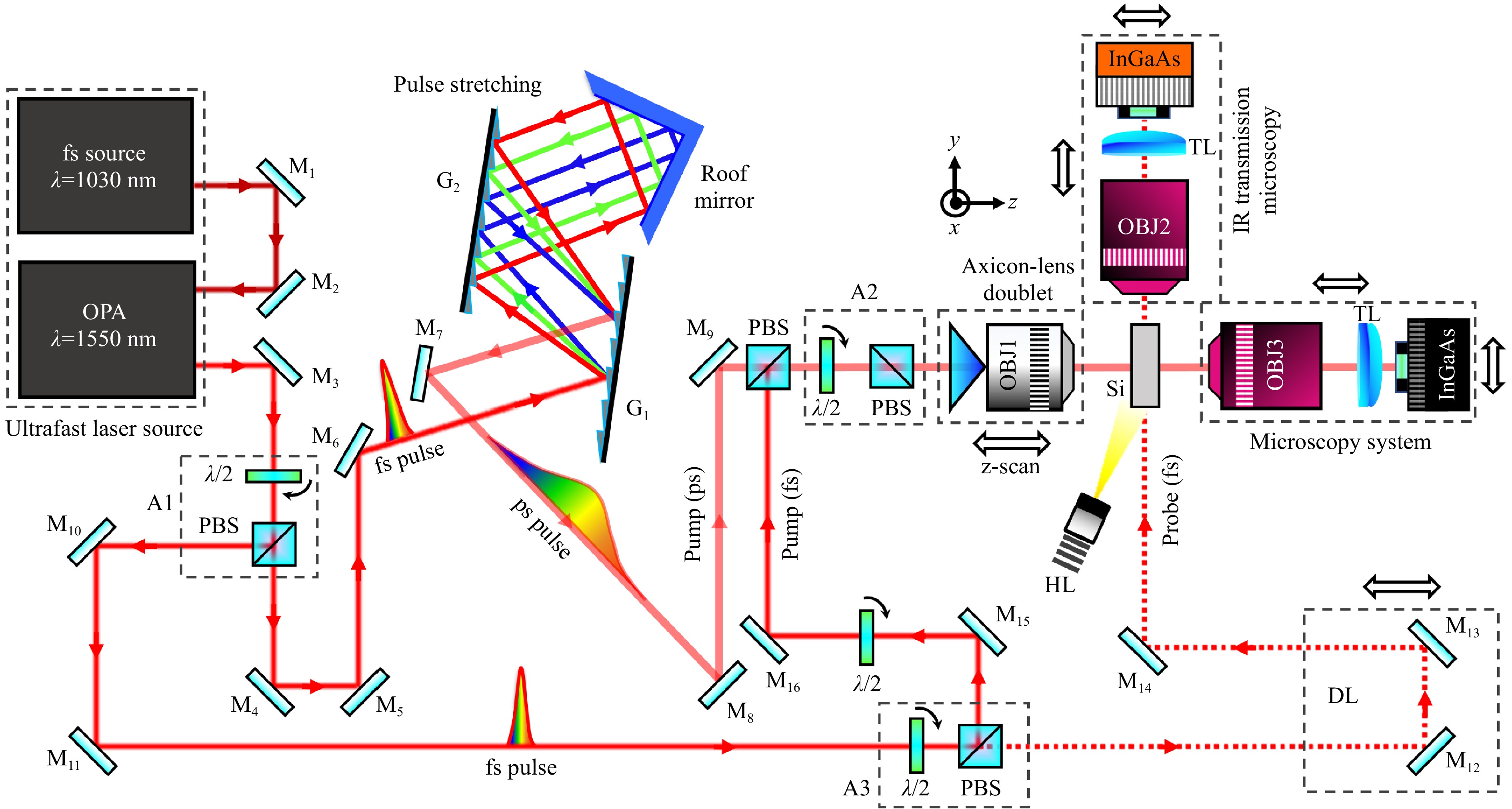
Fig. 3 Schematic diagram of the experimental setup used to study the formation of high-aspect-ratio structures inside c-Si with high-angle pseudo-Bessel micro-beams. This includes infrared microscopy diagnostics to characterize the applied beams, detect permanent modifications, and make time-resolved in-situ observations (pump-probe) of the laser-induced microplasma channels in the bulk of c-Si. The red arrows indicate the direction of laser propagation. OPA: optical parametric amplifier, M: gold mirror, G: reflective grating, $ \lambda $/2: half-wave plate, A: attenuator, PBS: polarized beam-splitter, OBJ: objective lens, HL: halogen lamp, TL: tube lens, DL: delay line.
The horizontally polarized pump beams (picosecond and femtosecond) are used separately but both are tightly focused in the bulk of intrinsic c-Si wafers (~1 mm thickness, orientation (100), Siltronix) using axicon-lens doublets. While we have tested different doublet combinations using objectives up to 0.85 NA, we concentrate here on the same arrangement as the one described before, that is a positive axicon with $ \alpha $ = 2° (Altechna) and a 0.45 NA objective lens (OBJ1, Olympus LCPLN20XIR). Accounting for the energy losses along the optical path, the maximum available pulse energies ($ E $) are 18.5 μJ and 43 μJ, for the picosecond and femtosecond pump beams, respectively, suitably adjusted using an attenuator (A2). All pulse energies in this report are those measured just before the focusing doublet, which has an associated energy loss of ~35%. For precise relative 3D positioning, the axicon-lens doublet and the sample are mounted on linear motorized stages allowing their displacement along the $ z $ axis. The sample motion is further controlled by motorized stages allowing micrometric control in the $ x $–$ y $ axis for repeated irradiation experiments. The compensation of the spherical aberration value when irradiating the c-Si sample has been the subject of a specific study (not shown) but did not reveal any significant difference in the observed processing responses. This tends to directly confirm the above-mentioned robustness of the produced beams to aberration. However, to avoid discussions, we have chosen in this paper to work with a fixed c.c. value of 0.6 mm corresponding to a precompensation for the middle (mid-depth) of the studied samples. To always make possible 3D beam focus analyses similar to those presented in the previous section under the conditions of the sample irradiation experiments, an infrared microscopy system is implemented along the pump beam optical axis as shown in Fig. 3. The system comprises a high NA long working distance imaging objective (OBJ3, Mitutoyo 100x/ 0.70 NA) and a tube lens (TL) of focal length 200 mm. The images of the beam profiles are recorded on this system with a high-resolution InGaAs array sensor (Raptor, OWL 640).
The reference focusing position ($ z $ = 0) for irradiation experiments with the pseudo-Bessel beam is taken when approaching the focus to the surface and scattered plasma radiation is detected from the lateral infrared transmission microscopy system shown in Fig. 3. Then, the beam focus is positioned at the desired depth ($ z=d $) inside c-Si by moving the axicon-lens doublet toward the sample by $ d/n_{si} $, where $ n_{Si} $ = 3.5 is the refractive index of c-Si at 1550 nm wavelength. The same lateral microscopy system is employed to capture the longitudinal cross-sectional images of the laser-induced modifications formed inside c-Si for beams with different irradiation conditions. In this case, the sample is illuminated with a halogen lamp (HL, OSL2IR fiber illuminator, Thorlabs) at a small angle from the side edge surface along the probe axis. Subsequently, the amplitude transmission images of the modifications are acquired using an InGaAs array sensor (Xenics, Bobcat 320 GigE 100 Hz) mounted on the optical arrangement comprising a long working distance imaging objective (OBJ2, Mitutoyo 10x/ 0.26 NA) and a TL of focal length 200 mm.
For further optical characterization of written modifications, we rely on an ex-situ custom microscope used for quantitative phase imaging (not shown). In brief, it consists of a configuration based on a Mach-Zender interferometer combined with an imaging arrangement and a 1317 nm light-emitting diode as the illumination source. More details of this setup developed in our previous work can be found in Refs. 41,14. Important for technological considerations, the system allows us to evaluate the refractive index change $ \Delta{n} $ associated with the produced structures.
In addition, to assess energy deposition and interaction dynamics inside the materials below the writing threshold condition, the lateral infrared transmission microscopy system is further utilized for time-resolved in-situ observations of the elongated microplasmas formed by nonlinear ionization inside c-Si. By varying the femtosecond-probe (horizontally polarized) delay line (DL) position, we obtain snapshots at different delays allowing us to determine the peak carrier densities and temporal evolution of the microplasmas for the picosecond and femtosecond pump irradiations, respectively. This approach gives insights into the dynamic behavior of the ionization characteristics induced by different pump-irradiation conditions.
-
Laser-induced high-aspect-ratio structures in c-Si require optimized laser-irradiation conditions in space but also in the temporal domain. To achieve permanent modifications, the use of relatively long pulses is usually beneficial to reduce the beam peak power, and consequently, the detrimental nonlinear and plasma effects preventing strong energy localization35. However, given the remaining uncertainties on the optimum pulse duration and even more for beam-shaped interactions, we have first implemented our axicon-lens doublet as a focusing element for 200-fs and 50-ps pulses (as shown in Fig. 3) but also for $ \leq $ 5-ns pulses from a fiber laser (not shown). This preliminary work allowed us to individually evaluate the ability of all these beams for in-volume processing of c-Si. While all the tested beams could achieve surface refractive-index modifications, we confirm that only the picosecond and nanosecond lasers were producing modifications deep inside the materials. Under repeated irradiation, we observed higher performance in precision and uniform channel processing for the picosecond regime. This optimal case was consistent with a previous work revealing a minimum energy threshold for in-volume writing with Gaussian beams for pulse duration ~20 ps or above35. From these considerations, we decided to concentrate on the use of picosecond pulses for material modification.
For these studies, the 50-ps pseudo-Bessel beam focus was first positioned at a depth $ d $ = 600 μm (where $ d $ = $ n_{si} \; \times $ displacement of focusing doublet in air) under the surface of the c-Si sample (depth corresponding to the chosen c.c. setting for non-aberrated beams, see before). The schematic of the writing arrangement is shown in Fig. S4 of the Supplementary Information. For laser exposure with pulse energy above the modification threshold ($ E_{th} \; \simeq $ 12.9 μJ), we immediately observe the laser writing of long channels of modified materials (> 100 μm) with diameters of a few micrometers, as can be seen in Fig. 2a. While we do not work in a laser ablation regime creating void channels, an analogy can be made with the so-called laser percussion drilling method42, to describe this process. Indeed, we do not obtain a modification from the first pulse deep inside the material. Instead, we observe in our case a surface damage initiated by the first applied pulses followed by a modification that self-propagates shot-after-shot longitudinally inside the material without any beam displacement. This leads to the formation of high-aspect-ratio vertical microstructures deep inside c-Si, where the crystalline nature of Si is changed but no void can be inferred. By repeating these experiments for different incoming pulse energies, it is interesting to note a range of energies ($ E<E_{th} $) where surface modifications remain present but without forming deep structures (see Fig. S2 of the Supplementary Information). The latter, combined with the absence of modification when tentatively creating direct modification in the bulk (for instance with a focused Gaussian beam below the surface as in Fig. S3), tend to indicate a peculiar laser writing process with two requirements: a sufficient level of intensity in the bulk and the formation of precursor defects created by front-surface damage with the applied pseudo-Bessel beam.
To further investigate the process, we study more precisely the dependence of the induced modification on the number of applied laser pulses. The microchannel modifications are fabricated inside c-Si for gradually increasing number of laser pulses $ N $ up to 20,000 at the maximum available pulse energy of 18.5 μJ and $ d $ = 600 μm, as presented in Fig. 4a. The separation between adjacent microchannels is 40 μm. In all cases, the modifications always initiate from front-surface damage and then grow on a pulse-to-pulse basis deep inside c-Si. Interestingly, the microscopy images of these percussion-written structures reveal some inhomogeneities and imperfections but the lateral dimension remains relatively constant along high-aspect-ratio structures. Such characteristics together with the nature of the accessible material modifications will define the range of potential applications. Fig. 4b shows the variation of the microchannel length (L) as a function of $ N $. It clearly highlights a nonlinear dependence due to a writing process for each individual pulse which depends on the modification achieved by the previously applied pulses as well as on the local intensity delivered near the pre-modified zones.
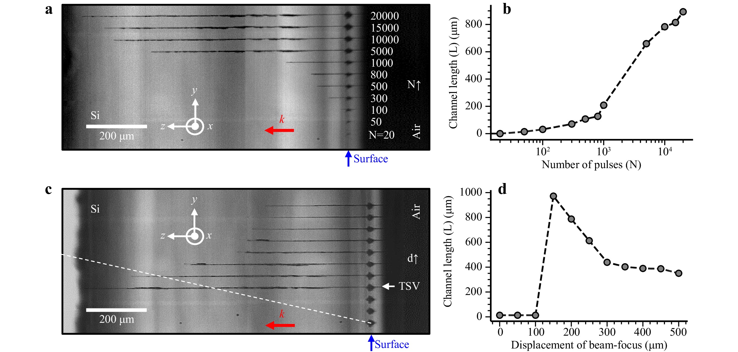
Fig. 4 Fabrication of high-aspect-ratio structures deep inside c-Si using repeated irradiations of the 50-ps pseudo-Bessel micro-beam from the axicon-lens doublet at 18.5-μJ pulse energy. a Side-view transmission image ($ y $–$ z $ plane) of written structures for an increasing number of applied laser pulses ($ N $) at $ d $ = 600 μm. $ k $ represents the writing laser propagation direction. The separation between adjacent microchannels is 40 μm. b Variation of microchannel length (L) as a function of $ N $. c Side-view transmission image of written structures with $ N $ = 20,000 pulses for different focusing depths. The white dashed line indicates the variation of the relative on-axis peak intensity position of the elongated Bessel-like filament from line to line. d Variation of the microchannel length (L) as a function of the displacement of the beam focus in air utilizing the focusing doublet.
To study the effect of varying on-axis intensity distributions inside the material, we have repeated the modification writing experiments for different focusing depths ($ d $) starting from the front surface and moving progressively toward the back surface of c-Si, and more. The writing procedures use the same pulse energy $ E $ = 18.5 μJ and a fixed number of applied pulses, $ N $ = 20,000. The produced modifications are shown in Fig. 4c (bottom to top). The $ z $-scan is done by displacing the axicon-lens doublet with an interval of 50 μm (in air) toward the sample, where the separation between adjacent microchannels is maintained at 40 μm. For a better interpretation, a guiding line between contiguous modifications during the $ z $-scan procedure is shown by a white dashed line, indicating the variation of the relative on-axis peak intensity position of the elongated Bessel-like filament from line to line. This immediately reveals a complex writing process leading to modifications that do not directly imprint the measured intensity distributions of the pseudo-Bessel beam, because the produced structures absolutely do not translate with the translating beam. Notably, no microchannel modifications are initiated inside c-Si for $ d\leq $ 350 μm even though surface damages are clearly detected. However, above this limit, the longest achievable channel (through modification) is immediately obtained for $ d\simeq $ 525 μm. In the former case, the absence of bulk modifications following the beam motion is attributed to inappropriate precursor formation since the surface becomes severely damaged when the peak intensity is close to the front surface. When $ d $ is further increased after the longest channel formation, the length of the channels consequently diminishes (see Fig. 4d) due to the decrease in the delivered intensity levels. However, it is informative to note that we observe some channels are formed inside c-Si for $ d $ values beyond 2 mm (equivalent distance in c-Si, or 0.55 mm in air). This immediately confirms the existence of very long beam intensity distributions at a sufficient intensity level for material modification with our axicon-lens doublet configuration (see Fig. 2).
An important observation with these laser writing experiments is remarkable through-wafer microchannel modification obtained in c-Si for $ d $ = 525 μm (shown in Fig. 4c). To evaluate the aspect ratio of the structure, a measurement of the lateral dimension is in principle needed. This can be difficult for structural changes (those in the present work), not morphological as we will see later on. For this reason, we have considered that the lateral size of the microstructures is typically comparable to the measured spot size (~1.5 μm at FWHM) of the pseudo-Bessel beam at its peak on-axis intensity position. This is consistent with estimates from the employed IR transmission microscopy images (Fig. 4 and Fig. S8 in Supplementary Information) as all the measured transmission profiles are < 3 μm (at FWHM). This corresponds well to the resolution limit of the measuring instruments. Accordingly, an aspect ratio of ~700 is estimated for the generated structure. This is comparable to the aspect ratio demonstrated with Bessel beams in dielectrics30, which has not been demonstrated in Si yet. It shows the effectiveness of our approach utilizing the axicon-lens doublet in conjunction with picosecond laser-irradiation, giving access to a novel percussion writing approach that differs from writing processes in dielectrics. In addition, it highlights the benefit of using axicon-lens doublets to produce high-angle pseudo-Bessel beams that are laborious to obtain with 4f-telescopic systems. The latter is the most common approach used in laser-material processing to produce micro-Bessel beams and constant-intensity filaments. Interestingly, the spatial characteristics (lateral and longitudinal sizes) of the beams from the doublet method can be comparable. However, as can be seen with Fig. 2d, the method will hardly compete with the standard approach if a constant intensity is desired. It remains that in the specific studied case here, we actually anticipate an advantage with the intensity distribution produced by doublet focusing. The multishot percussion writing must take benefit from the rising on-axis intensity profile with depth for compensating increasing screening effects with processing depth. Depending on the type of produced modifications associated with this writing process, this observation may pave the way to unique monolithic solutions for new optical TSV technologies, an aspect that will be discussed later on.
-
To assess the characteristics of the studied interactions with our pseudo-Bessel beams in the bulk of c-Si, we study the spatiotemporal dynamics of the elongated microplasmas induced by the picosecond and femtosecond pulses. For this investigation, we rely on the time-resolved pump-probe microscopy technique.
The schematic of the configuration used for infrared transmission imaging of the produced microplasmas is depicted in Fig. S5 of the Supplementary Information. Recording high-resolution plasma images requires uniform probe illumination on the sample. Therefore, a difference here in comparison to the writing experiments is that we strategically position the sample with its optically-polished flat wider surface oriented toward the femtosecond-probe beam, while the pump beam is focused inside the material through its 1-mm thick cleaved edge. An important observation with this configuration is the incapacity of writing deep structures even using the same picosecond pseudo-Bessel beam used to repeatedly produce microchannels in previous experiments (at E ~ 18.5 μJ, $ N $ = 20,000 pulses). Geometrically, the 1-mm thickness is expected not to limit the pump beam at the sample entrance, so we attribute this difference to the presence of some scattering at the edge of the samples obtained by cleaving the wafer and/or an eventual contribution of a signal from the back-surface reflection for writing. Despite this difference, we expect the essential characteristics of the interactions to remain accessible by our pump-probe study and a relative comparison of the plasma responses can be made between the two temporal regimes.
With these conditions, we investigate the dynamics of the microplasmas when positioning the pseudo-Bessel beam focus typically at $ d\simeq $ 600 μm inside c-Si, for the picosecond and femtosecond pump irradiations with fixed pump-probe delays at 83 ps and 13 ps, respectively. As we will see later on, these delays correspond to the measured shadowgraphy images evidencing the peak plasma density conditions (end of pulses before plasma decay). The measured transmission images of the microplasma channels are shown in Fig. 5a for both pump-irradiation conditions at E ~ 18.5 μJ. The absence of permanent modification for both considered cases allows us to work with increased camera exposures so that averaging over many shots can be used to improve the signal-to-noise ratio (exposure was set typically at 40 ms, corresponding to 40 applied pulses at 1 kHz).
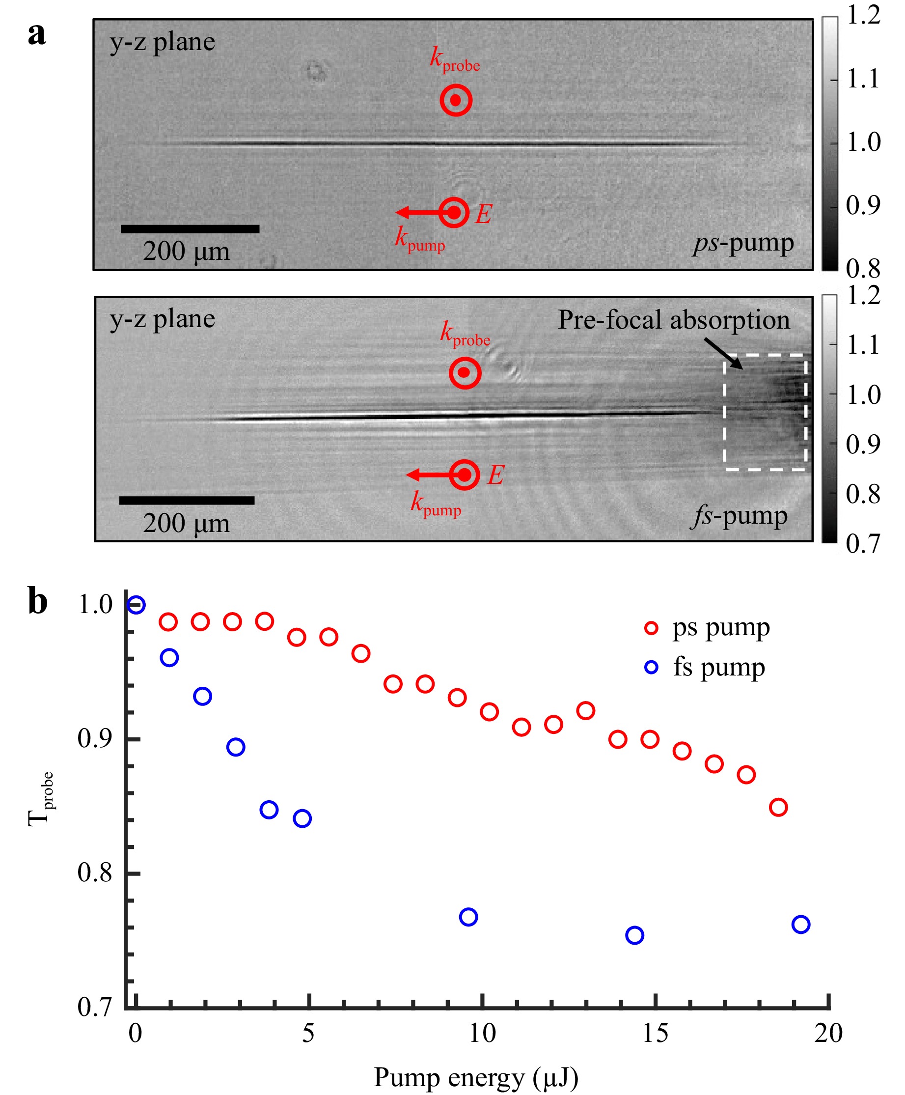
Fig. 5 a Time-resolved shadowgraphy images of the elongated microplasmas formed inside c-Si by picosecond and femtosecond pulses focused with the axicon-lens doublet at $ d \; \simeq $ 600 μm below the surface. The same pulse energy E ~ 18.5 μJ below the modification threshold is used for both beams. b Probe transmission level at the center of the produced microplasmas as a function of the pump energy. To observe peak density plasma conditions, the pump-probe delays are fixed respectively at 83 ps and 13 ps for the picosecond and femtosecond pump irradiations.
Remarkably, both pump beams are capable of producing similar elongated microplasmas deep inside c-Si. However, significant surrounding side-lobe interactions of the beam are visible for the femtosecond pump (horizontal stripes). In addition, significant ionization is also revealed in the pre-focal zone for this interaction regime (highlighted by a white dotted box). The latter is attributed to pre-focal absorption of the beam by highly efficient two-photon absorption given the relatively high peak intensity of the femtosecond pump. These observations indicate that the limitations reported in the literature on the achievable beam power and energy density inside c-Si with femtosecond Gaussian1, and conventional Bessel beams28, surely persist with the pseudo-Bessel beams of this work. It also supports the observed incapacity of the ultrafast regime to achieve in-volume permanent modifications in all tested cases. On the contrary, the absence of such features in the collected image for the tested picosecond interaction is taken as evidence of sufficient pulse stretching to decrease the peak intensity at a level where the detrimental nonlinearities outside the high-intensity light filament are suppressed. However, it is very interesting to note that a well-contrasted plasma string remains observed across the high-intensity region. This likely indicates a relatively good trade-off with peak intensity still leading to a large nonlinear ionization yield in c-Si.
To further study the interaction limitations, we measure the delivered intensity levels. With the transmission microscopy systems shown in Fig. 3, we image the pseudo-Bessel focus at the flat-polished back surface of the c-Si sample (under ideal orientation as in the writing experiment). Measurements are repeated for varying pump energy levels and the corresponding results are shown in Fig. S6 of the Supplementary Information. Similar to the probe transmission measurement (see Fig. 5b), a very pronounced clamping of the delivered peak intensity is observed for the femtosecond pump, whereas the picosecond pump shows an almost linear response with increasing values of energy. This confirms that the excitation saturation relies directly on the optical limitation on the delivered peak intensity in the bulk of c-Si due to strong propagation nonlinearities, as it was similarly observed in previous works using Gaussian5 or Bessel beams28. In addition to intensity clamping, the femtosecond pump also displays significant beam distortions at high energy values. In contrast, the picosecond pump remains entirely free from beam distortions even at high energy values. The contrasting beam stability for these two different pump irradiations provides invaluable insights into their distinct pre-focal interaction dynamics within c-Si over the studied range of energy levels. These findings confirm the potential robustness of utilizing the picosecond regime to deliver higher energy densities for processing inside c-Si than the femtosecond one.
To quantify the generated free-carrier densities ($ N_e $) in c-Si, we can rely on the measured probe transmission levels found at the center of the microplasmas from the collected images. According to the Drude model43, the complex refractive index $ \tilde{n} $ can be expressed by, $ \tilde{n}^2 $ = $ n_{0}^2 $ − $ {\omega_{p}^2}/({\omega^2 + i\gamma\omega} )$, with the plasma frequency defined as $ \omega_{p} $ = $ \sqrt{{N_{e}e^2}/{\epsilon_{0}m^*}} $ where $ e $ is the electron charge, $ \omega $ is the laser frequency, $ \epsilon_{0} $ is the free-space permittivity, $ \gamma $ is the collision frequency and $ m^* $ = 0.18$ m_e $ is the effective electron mass for low-density plasma in c-Si44. In our calculation, we use $ \gamma $ = 0.3 fs−1 which corresponds to a rate dominated by electron-hole collisions and reasonable for low to intermediate excitation densities45. For a homogeneous plasma, the probe transmission $ \mathrm{T_{probe}} $ can be simply described by the Beer-Lambert law, $ \mathrm{T_{probe}} $ = $ \mathrm{exp}((- {4\pi Im(\tilde{n})}/{\lambda})d_{plasma}) $, where $ \lambda $ is the probe wavelength, $ d_{plasma} $ is the lateral dimension of the microplasma channel, and $ \operatorname{Im}(\tilde{n}) $ represents the imaginary part of the refractive index which can be expressed by, $ \operatorname{Im}(\tilde{n}) \; \simeq \; {\gamma \omega_{p}^2}/ ({2\omega^3(1 + \gamma^2/\omega^2)}) $. In principle, $ d_{plasma} $ can be directly evaluated from the images by extracting the vertical dimension of the plasma according to its cylindrical symmetry. However, the obtained values evidence a situation limited by the resolution of our imaging system ($ \approx\;2 $ μm). For this reason, we systematically consider $ d_{plasma}=1.5\; $ μm for all these estimations. This corresponds to the measured spot size of the pseudo-Bessel focus in air (see Fig. 2c).
The variation of the probe transmission level as measured at the center of the produced microplasmas inside c-Si is presented in Fig. 5b, as a function of the pump energy. Notably, the picosecond pump exhibits a progressive decrease of $ \mathrm{T_{probe}} $ with the increasing value of pump energy (nearly linear change in the range of considered energies). In contrast, in the case of the femtosecond pump, there is a more pronounced drop of $ \mathrm{T_{probe}} $ that tends to remain constant for energies exceeding ~10 μJ, thus revealing a stronger ionization reaching a saturation inside c-Si. Taking the minimum probe transmission ($ \mathrm{T_{min}} $) levels measured at ~85% and ~75%, the estimated peak free-carrier densities $ N_{e, max} $ are $ 9.6 \times 10^{18} $ cm−3 and $ 1.7 \times 10^{19} $ cm−3 for the picosecond and femtosecond cases, respectively. Both of these values are significantly below the critical plasma density $ N_{crit} $ at 1550 nm ($ \simeq 4.6 \times 10^{20}$ cm−3), and so intrinsically below the condition for optical breakdown in the bulk of c-Si. However, it is important to note that relatively similar levels of excitation densities are reached for both regimes. This shows immediately a major specificity in comparison with surface processing studies where shorter and more intense laser pulses usually lead to stronger ionization and so decreased modification thresholds. Such situations definitively do not directly translate for semiconductor bulk experiments. Much higher energy deposition would be immediately expected by two-photon ionization ($ \propto I^2 $) with intense femtosecond pulses46. The modest difference observed here indicates that the delivered intensity is actually lowered by nonlinear propagation effects in the bulk for the femtosecond regime and/or collision-assisted ionizations (including impact and avalanche mechanisms) contribute to compensating the lower intensity in the picosecond regime. Moreover, it is striking to note that a stronger ionization is obtained with the femtosecond pulses but it is the picosecond pulses that have shown a better ability for writing. This immediately reveals that the free-carrier density is not the most appropriate criterion to define a modification threshold. The deposited energy density should then be considered.
Rigorously, there exists no direct relationship between the absorbed laser energy density ($ E_{abs} $) and $ N_{e} $ considering the band gap $ E_{g} $ for the ionization energy. One should also account for the mean kinetic energy ($ \langle E_{k} \rangle $) associated with the acceleration of free-carriers by the laser field, also called Joule heating of the plasma by inverse Bremsstrahlung absorption (IBA). Fig. 6a, b display the time-evolution of $ \mathrm{T_{probe}} $ at the center of the produced microplasmas as a function of the pump-probe delays measured at a fixed energy $ E\sim $ 18.5 μJ for our picosecond and femtosecond pump irradiations, respectively. It shows that the transient linear absorption of the plasma by IBA grows progressively across the temporal range of the pump irradiations (indicated by shaded regions in the plots). It also reveals a decay time for both cases in the nanosecond time scale, which is consistent with a previous work concentrating on this question47. This makes it reasonable to ignore relaxation and/or carrier diffusion as energy dissipation processes during the pulse. Taken together, the synchronized measurement of the laser field and absorption of the plasma must then show the potential to store energy in the electronic system during the pulse (by integration). However, with a pump and a probe of identical duration, the time resolution is insufficient for this assessment with the femtosecond pulse.
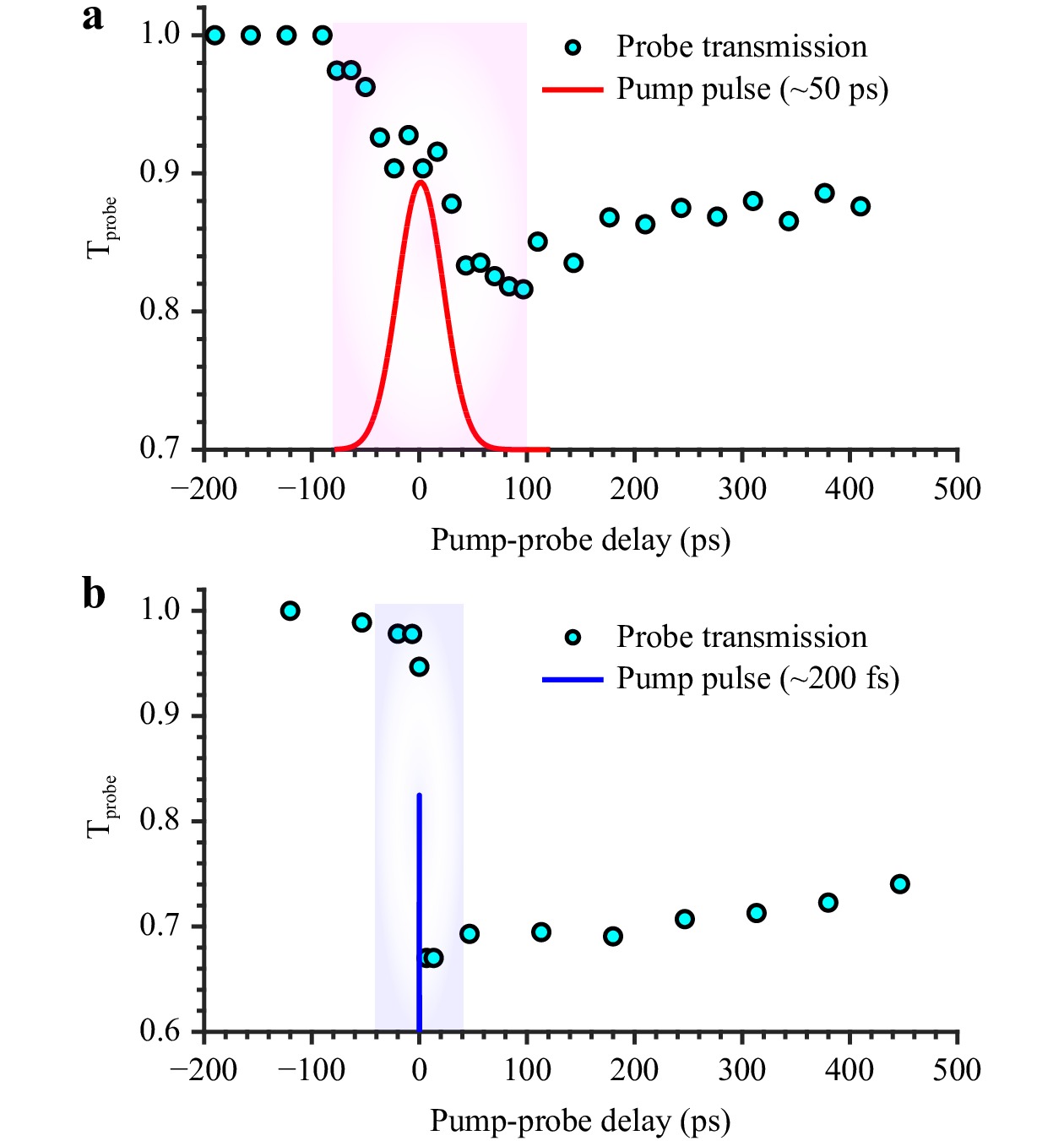
Fig. 6 Probe transmission levels measured at the center of the produced microplasmas inside c-Si induced by a picosecond, and b femtosecond pumps as a function of the pump-probe delays for $ d\simeq $ 600 μm and at E ~ 18.5 μJ. The shaded regions highlight the time scales over which the transient evolution of the plasma absorption occurs.
To highlight the expected difference between the two cases, it remains important to remember the collision-based nature of IBA process behind linear energy deposition. The expected collision times accounting for carrier-carrier (see above) and carrier-phonon collisions are typically in the range of 1 fs to 1 ps, which remain orders of magnitude shorter than the interaction time with our 50-ps pulse. Thus, one can expect sequential absorption events leading to more carrier acceleration and energy accumulation in the produced plasma with this pulse in comparison to the femtosecond pulse. This is also consistent with the nonlinear ionization description stated before. To tip the scales in favor of impact as compensation for the decreased photoionization with long pulses, one must necessarily rely on energetic electrons and so a requirement is an electron distribution developing towards higher energy states in the conduction band (higher electron temperatures $ T_e $). Obviously, a rigorous model should account for important dependencies of the different physical mechanisms to numerous varying parameters (for instance, $ N_e $, $ T_e $, or lattice temperature). However, this qualitative description given here appears to be consistent with the observations associated with different pump-irradiation cases. Overall, an important conclusion here is that the generation of microchannel modifications (see Fig. 4) by percussion writing relies on the presence of precursor defects in the vicinity of relatively hot plasma conditions. In our experiments, these conditions are created over extended dimensions inside c-Si only with sufficiently long-ionizing laser pulses.
-
The application perspectives of high-aspect-ratio structures obtained with axicon-lens-focused picosecond pulses inside c-Si will depend on the type of refractive-index modifications that can be obtained along the produced microchannels. To treat this question, we first use defocused infrared transmission imaging. At first, repeatable microchannels are fabricated inside c-Si under the identical laser condition of $ d\simeq $ 600 μm, $ E\sim $ 18.5 μJ, and $ N $ = 20,000 pulses. The infrared microscopy images of those structures (Fig. 7) are then obtained using the arrangement described in Fig. S7 of the Supplementary Information.
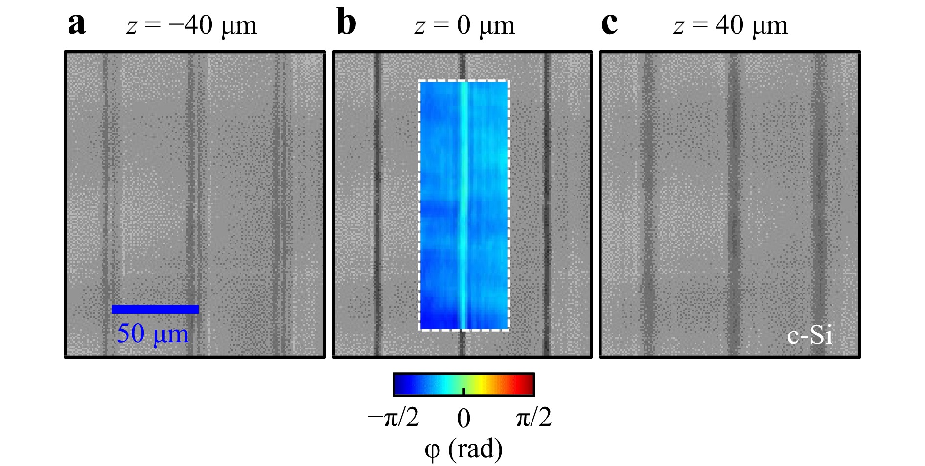
Fig. 7 Infrared transmission microscopy imaging of the microchannels fabricated inside c-Si using the axicon-lens doublet under identical conditions ($ d\simeq $ 600 μm, E ~ 18.5 μJ, and $ N $ = 20,000 pulses). The transmission images are obtained at different focusing depths of the imaging system by a translating the object 40 μm from the focal plane in the direction away from the camera, b at the focal plane, and c translating the object 40 μm from the focal plane toward the camera. The inset represents the retrieved phase image of the microchannel modification using quantitative phase microscopy, showing a positive refractive index change. Only the central part of the fabricated structures is displayed.
A set of collected images is shown in Fig. 7. At the best focus plane (i.e. at z = 0 μm) the structures appear as dark lines (Fig. 7b) evidencing relatively lossy structures due to absorption or scattering. While it is not a pure phase object, which would have been nearly invisible at this best focus plane, the out-of-focus images (i.e. at z = ±40 μm) exhibit characteristic features that allow us to discuss the sign of the apparent index change associated with the modifications. An intensity contrast is observed at the central part of all the modifications, becoming bright and dark when translating the object 40 μm from the focal plane in the direction away from the camera (Fig. 7a) and 40 μm toward the camera (Fig. 7c), respectively. This characteristic behavior is identical for all the fabricated structures. This optical response is equivalent to an observation through a cylindrical focusing lens, thus indicating a positive refractive index change ($ \Delta{n} > 0 $) for the laser-modified cylindrical regions with respect to the pristine c-Si.
For a quantitative analysis, we turn to the phase microscopy setup described in the Experimental setup section. By acquiring four phase-shifted interference images ($ S_k $), a quantitative phase image is directly reconstructed using the expression, $ \varphi $ = arctan$ [(S_4-S_2)/ (S_1-S_3)] $. An example of the retrieved phase image for the laser-modified region obtained with this procedure is shown in the inset of Fig. 7b. In comparison to the background (arbitrary phase level), it reveals a positive phase variation $ {\Delta{\varphi}}\simeq $ 0.63 rad, which is relatively uniform along the long modified area. This allows us to evaluate the average refractive index change by, $ \Delta{n} $ = $ \lambda {\Delta{\varphi}} / 2 \pi D $, where $ \lambda $ = 1317 nm is the operating wavelength of the interferometer, and D = 1.5 μm is taken for the diameter of the modifications. This leads to a positive index change $ \Delta{n} \; \simeq $ 8.7 × 10⁻². While uncertainties persist on the precision of this estimation due to the resolution limitation of our infrared microscopy system to evaluate the structure diameter, this corresponds to a very high refractive index change ensuring light-guiding capabilities for the produced modifications (inset of Fig. 7b). Indeed, this value is even higher than the index change values reported in recent works demonstrating the fabrication of waveguides inside c-Si by scanning the Gaussian focus of nanosecond14,16 or picosecond laser beams48, and interpreted in most cases by a partial amorphization of c-Si.
Numerous waveguiding modifications produced under identical conditions were characterized by the same procedure, all exhibiting similar refractive index change values (not shown). This shows the repeatability of our percussion writing procedure, which does not need any beam motion for longitudinal writing of waveguides. The writing procedure also offers an advantage of precision as the lateral dimension of the reported structures is significantly smaller than those previously demonstrated in waveguide studies14-16,48. This opens the door for the direct fabrication of optical TSV structures holding potential for vertical optical interconnections in future high-density ultrafast multilayer chips based on Si-photonics.
-
Through-wafer vias or void formation similar to what can be observed in dielectrics by means of percussion drilling and/or microexplosion30,42, have not been achieved in our experiments due to insufficient space-time energy confinement inside c-Si. This would be highly desirable with the same resolution as the one we have demonstrated for waveguide writing in order to create high-density vertical interconnects in chips after metal deposition in the through-holes. While this remains so far inaccessible by any laser methods in c-Si and any other semiconductors, the observations made on the plasma strings could inspire future physics experiments and the advent of new technologies in the field of ultrafast microelectronics.
A unique phenomenon observed thanks to the configuration of this experiment, is the propagation of the plasma-front during the creation of the ionized microchannels in the bulk of c-Si when using the femtosecond pump excitation. Fig. 8 shows the shadowgraphy images of the forward propagation track of such plasma-front at varying pump-probe delays. According to this transient evolution, the plasma string of ~700 μm length (the standard thickness of Si wafers in microelectronics) is fully deployed and established within about ~7.3 ps, orders of magnitudes faster than the plasma decay47. Notably, this time scale is also significantly less than the pulse duration of the stretched picosecond pulses studied in this work making such a process impossible to resolve with the writing beam.
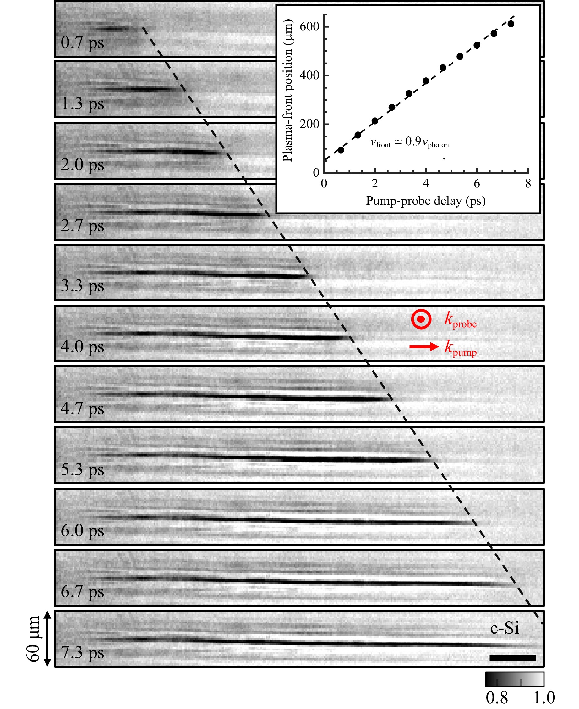
Fig. 8 Time-resolved shadowgraphy images evidencing near-luminal propagation of the plasma-front in the bulk of c-Si during the ionization process with femtosecond pulses focused with axicon-lens doublet. Inset represents the measured positions of the plasma-front as a function of pump-probe delay. The dashed lines are made to guide eyes, indicating a constant propagation approaching the speed of light ($ v_{photon} $) inside c-Si. The scale bar is 60 μm.
Interestingly, analyses of the images allow us to estimate the propagation velocity of the plasma-front. As can be seen in the inserted graph of Fig. 8, the front propagates at a nearly constant velocity estimated at $ v_{\mathrm{front}}\simeq $ 0.9 $ c/n_{Si} $, with $ c $ being the velocity of light in vacuum. Given the beam-shaping method based here on adding an axicon to a focusing objective lens to distribute the different angular components along the optical axis, it is interesting to observe that a near-luminal propagation can be obtained. This velocity can also reasonably be adjusted depending on the designed geometry (e.g. different axicon angles) opening the door to achieve inside-semiconductor advanced physics experiments (THz generation, photon acceleration), which are today only limited to gases49,50.
For technological considerations, we can expand on the achievable transient local electrical properties with the formation of plasma strings. In doing so, it is essential to first refer to the free-carrier density measured in the previous section at > 1019 cm−3. This corresponds to an excess of free-carriers of very high concentration in comparison to conventional Si doping levels (n- or p-type) in the sector of microelectronics. Our initial intrinsic c-Si wafers have a specified resistivity of > 200 Ω·cm corresponding to an apparent carrier density on the order of ~1013 cm−3 from defects according to the doping abacus used in the domain. With the free-carrier injection by ultrafast ionization, we then expect a local drop of the resistivity down to ~5 × 10⁻³ Ω·cm. Thus, these significantly conductive plasma strings can constitute vertical electrical connections that can interestingly be switched on-off and modulated optically. According to the 7.3-ps time measured for the through-silicon plasma formation and the typical 2-ns decay time of microplasmas in c-Si (see Ref. 47 and Fig. 6), this supports the vision of a unique monolithic technology for vertical electrical interconnections in Si-chip stacks which are optically controllable at near GHz repetition rates.
-
To the best of our knowledge, we have applied for the first time an axicon-lens doublet focusing system in the context of laser-material processing. We have shown that it can represent an efficient beam-shaping approach to produce pseudo-Bessel beams with extremely high angular components. The obtained beam characteristics are highly desirable for semiconductor processing applications. Investigating various control parameters, we have shown that picosecond laser pulses (at 1550 nm) focused with the doublet inside c-Si can initiate a percussion writing modality which has not been reported yet. The resulting permanent refractive-index modifications achievable with this writing process relies on the formation of appropriate precursor defects in the vicinity of relatively hot plasma conditions only provided with sufficiently long pulses. While the underlying mechanisms are only partially understood, the potential influence of surface modification on the writing beam propagation should be considered and analyzed in future works. In the studied cases, we have shown that the same beam can deliver these hot plasma conditions along channels through a standard Si wafer (thickness ~700 μm) while producing appropriate front-surface damage to seed the writing process. This leads to the fabrication of high-density ultra-high-aspect-ratio TSV-like permanent structures exhibiting a high positive refractive-index change of $ \Delta{n} \; \simeq \; 10^{-2} $ and aspect-ratio of ~700. With femtosecond laser pulses, we confirm intensity conditions intrinsically clamping under the threshold for permanent modification due to strong propagation nonlinearities, which persist with the produced pseudo-Bessel beams. However, we have demonstrated that relatively dense, well-contrasted, and conductive elongated plasmas can be formed along the high-intensity channels through the Si wafers. Taken together, these observations pave the way to a new range of solutions for ultrafast vertical communication channels (either optical or electrical) in Si-chips. In particular, the new modality to directly fabricate vertical optical waveguides with high-resolution is expected to have an immediate impact. Given the general trend to replace electrical signals with optical ones for high-speed and less-consuming microprocessor technologies, this holds high potential to serve directly in this context, and more generally in the rapidly growing field of silicon photonics.
-
This work was conducted using LaMP facilities at LP3. The project received funding from the French National Research Agency (ANR-22-CE92-0057-0, KiSS project) and the European Union’s Horizon 2020 research and innovation program under grant agreements No. 101034324 (MSCA-COFUND) and No. 724480 (ERC).
Ultra-high-aspect-ratio structures through silicon using infrared laser pulses focused with axicon-lens doublets
- Light: Advanced Manufacturing , Article number: (2024)
- Received: 02 November 2023
- Revised: 18 March 2024
- Accepted: 04 April 2024 Published online: 10 July 2024
doi: https://doi.org/10.37188/lam.2024.022
Abstract: We describe how a direct combination of an axicon and a lens can represent a simple and efficient beam-shaping solution for laser material processing applications. We produce high-angle pseudo-Bessel micro-beams at 1550 nm, which would be difficult to produce by other methods. Combined with appropriate stretching of femtosecond pulses, we access optimized conditions inside semiconductors allowing us to develop high-aspect-ratio refractive-index writing methods. Using ultrafast microscopy techniques, we characterize the delivered local intensities and the triggered ionization dynamics inside silicon with 200-fs and 50-ps pulses. While similar plasma densities are produced in both cases, we show that repeated picosecond irradiation induces permanent modifications spontaneously growing shot-after-shot in the direction of the laser beam from front-surface damage to the back side of irradiated silicon wafers. The conditions for direct microexplosion and microchannel drilling similar to those today demonstrated for dielectrics still remain inaccessible. Nonetheless, this work evidences higher energy densities than those previously achieved in semiconductors and a novel percussion writing modality to create structures in silicon with aspect ratios exceeding ~700 without any motion of the beam. The estimated transient change of conductivity and measured ionization fronts at near luminal speed along the observed microplasma channels support the vision of vertical electrical connections optically controllable at GHz repetition rates. The permanent silicon modifications obtained by percussion writing are light-guiding structures according to a measured positive refractive index change exceeding 10−2. These findings open the door to unique monolithic solutions for electrical and optical through-silicon-vias which are key elements for vertical interconnections in 3D chip stacks.
Research Summary
Shaped beams for the fabrication of vertical interconnections in next-generation silicon chips
Through-Silicon Vias (TSVs) are essential elements for 3D integration of high-performance electronic and optoelectronic devices. Machining with so-called Bessel beams is a relevant approach for producing high-aspect-ratio TSVs in dielectrics but not in semiconductors. Researchers at LP3, a joint laboratory between CNRS and Aix-Marseille University (France), made a critical step to deliver a technology for semiconductors. Elaborating a concept based on a simple combination of conical lenses (called axicons) and microscope objectives, they produced infrared pseudo-Bessel microbeams with high angles inaccessible with standard methods. Using appropriate ultrashort pulses, they found a percussion writing modality leading to extremely high-aspect ratio structures through silicon. The characteristics of the elongated microplasmas and subsequent material modifications created inside chips support a new range of solutions for ultrafast vertical communication channels (optical and electrical) in silicon chips.
Rights and permissions
Open Access This article is licensed under a Creative Commons Attribution 4.0 International License, which permits use, sharing, adaptation, distribution and reproduction in any medium or format, as long as you give appropriate credit to the original author(s) and the source, provide a link to the Creative Commons license, and indicate if changes were made. The images or other third party material in this article are included in the article′s Creative Commons license, unless indicated otherwise in a credit line to the material. If material is not included in the article′s Creative Commons license and your intended use is not permitted by statutory regulation or exceeds the permitted use, you will need to obtain permission directly from the copyright holder. To view a copy of this license, visit http://creativecommons.org/licenses/by/4.0/.

 DownLoad: