


-
With the rapid growth in use of data in artificial intelligence, 5G systems, cloud computation, and the Internet of Things, transmitters with extremely high capacities are required for data communication1-3. Ultrafast optical modulation is an important technology for high-capacity transmitters. In recent years, high-speed optical modulators have attracted considerable interest, and significant progress has been achieved using different mechanisms in various material systems4-16. Among them, optical modulators on a lithium-niobate-on-insulator (LNOI) platform have exhibited great potential, because of a linear electro-optic (EO) effect, low excess loss, and high stability17. In particular, LNOI EO modulators based on Mach-Zehnder interferometers and microresonators have performed excellently. For LNOI Mach-Zehnder modulators (MZMs)18-23, the length of the phase-shifting arms is typically several millimeters, or even centimeters, to realize a low voltage. Accordingly, traveling-wave electrodes have been introduced, along with high-speed MZMs with > 100 Gbps on-off keying (OOK) modulation22 and > 96 GBaud 16-QAM modulation23. However, due to their large footprint, arraying of LNOI MZMs is inconvenient for high-capacity multiplexed systems with multiple channels. In contrast, the resonator-based modulators of LNOI can be compact, which may reduce power consumption24-27. Meanwhile, it is possible to achieve a high modulation bandwidth by lowering the Q-factor to reduce the photon lifetime. Therefore, resonator-based LNOI modulators have attracted significant attention in recent years. In particular, we successfully demonstrated high-speed LNOI modulators based on a specific 2 × 2 Fabry-Perot (FP) cavity, enabling an ultra-high 3-dB bandwidth beyond 110 GHz and data capacity up to 140 Gbps28. More importantly, the footprint of the modulation section is as short as ~50 μm (much smaller than that of the reported LNOI ring resonator modulators24), which is very attractive for arraying wavelength-division multiplexing (WDM) systems.
Advanced multiplexing techniques have been widely studied to expand link capacity by transmitting data through multiple channels in parallel. In particular, WDM, in which multiple wavelength channels are introduced, has been successfully applied in recent decades. WDM filters play a key role in (de)multiplexing wavelength channels in corresponding systems29-31. For example, various waveguide structures have been developed in recent years to realize WDM filters with excellent performance, including arrayed-waveguide gratings (AWGs)32,33, ring resonators34-36, (cascaded) MZIs37,38, and waveguide Bragg gratings39-41. For these WDM filters, high-quality fabrication is critical for achieving low-loss and low-phase-error light propagation in optical waveguides. Currently, several typical fabrication technologies have been established for LNOI photonic waveguides, including chemical mechanical polishing42,43, wet etching44, and dry etching45,46. Among these, the dry-etching method is typically preferred because of its process compatibility and fabrication repeatability. Further, inductively coupled plasma (ICP) etching with Ar gas is one of the most common methods for fabricating LNOI photonic waveguides and devices.
However, for X-cut LNOI photonic waveguides (which are the most popular for optical modulation), non-negligible mode hybridization might exist in sharp waveguide bends47 or adiabatic waveguide tapers owing to the LN anisotropy and angled waveguide sidewalls. Thus, mode manipulation is challenging when light propagates through X-cut LNOI photonic integrated circuits (PICs). Furthermore, design of devices with LN anisotropy is inconvenient because accurate calculation of the accumulated phase delay is difficult in waveguide bends (which is usually indispensable in various PICs). Consequently, realizing compact and high-performance LNOI photonic devices, including WDM filters, remains complicated. For example, AWGs based on X-cut LNOI waveguides have not yet been reported because the structural design is quite complex owing to the anisotropy of the waveguide bends and free-propagation regions.
Nevertheless, great efforts have been made and impressive progress has been achieved utilizing smart designs without any waveguide bends in the key regions. For example, a four-channel coarse WDM transmitter chip on LNOI has been demonstrated utilizing a multiplexer including an angled multimode interferometer48, which is as long as nearly two millimeters and is unsuitable for cases with many channels and narrow channel spacing. In addition, the spectral responses are not flat-top; thus, the 1-dB bandwidth is relatively small. As an alternative, in our previous work, we proposed and developed an LNOI photonic silicon filter based on a straight multimode waveguide grating (MWG)49 that enables a box-like spectral response, and whose central wavelength and bandwidth can be designed flexibly50.
In this study, a four-channel WDM filter with box-like responses was established using cascaded LNOI MWGs for the first time. For example, four channels were included and the channel spacing was set to 20 nm. In addition, the four-channel WDM filter is integrated with a 1 × 4 array of FP-cavity modulators, which have a particularly ultra-short modulation region of ~100 μm. The introduction of the FP-cavity modulators enables energy-efficient and high-speed optical modulation. The proposed LNOI photonic chip, which has a total footprint as small as 0.3 × 2.8 mm2, can be used to realize four-channel WDM transmitters. Photonic waveguides and circuits of large scale present increased manufacturing requirements. With the advanced Ar ion etching process developed by ourselves, the chip features transport cascading and channel uniformity. Experimentally, the proposed chip enables high-capacity data transmission of 320 Gbps (4 × 80 Gbps) OOK signals and 400 Gbps (4 × 100 Gbps) PAM4 signals with the low power consumption of 11.9 fJ/bit. This indicates great potential for the large-scale photonic integration of LN, and the bright prospect of LNOI regarding its widespread use in integrated photonic devices.
-
Fig. 1a presents the configuration of the proposed LNOI photonic chip for four-channel WDM transmitters comprising four FP-cavity LNOI modulators, used to modulate light of different wavelengths accordingly (Fig. 1b). The modulated signals were then multiplexed using a four-channel WDM filter based on MWGs in a cascade (Fig. 1c).

Fig. 1 a Schematic of configuration of the proposed lithium-niobate-on-insulator (LNOI) photonic chip for four-channel wavelength-division-multiplexing (WDM) transmitters, comprising four FP-cavity LNOI modulators. b 2 × 2 FP-cavity optical modulator. c Stage of the WDM filter, constituting a mode (de)multiplexer and a multimode waveguide grating (MWG). Inset: cross section of an LNOI ridge waveguide.
Each MWG filter comprised a mode (de)multiplexer based on an adiabatic dual-core taper (with waveguides A and B) and an MWG, as shown in Fig. 1c. The inset depicts the cross section of the LNOI ridge waveguide with the sidewall angle of 30° (relative to the vertical axis). Here, we used a 400-nm-thick X-cut LNOI wafer, and the LNOI ridge waveguide had the etching depth of 200 nm and air up-cladding. As shown in Fig. 1c, the TE0 mode launched from the left port of waveguide B is converted to the forward TE1 mode at the right end of waveguide A through the mode (de)multiplexer based on the adiabatic dual-core taper. The forward TE1 mode is then converted very efficiently to the backward TE0 mode by the MWG when the wavelength satisfies the Bragg grating condition. One should note that the TE1-TE0 conversion is very efficient while the TE1-TE1 reflection is negligible for the MWG. Then, the backward TE0 mode is output with very low losses from the left port of waveguide A, realized with the mode (de)multiplexer.
The mode (de)multiplexer was designed according to the method described in a previous work51. The core widths at the input/output ends of waveguides A and B were chosen as (wa1, wa2) = (1, 2) μm, (wb1, wb2) = (0.6, 0.2) μm, the taper lengths (L01, L12, L23) = (50, 100, 50) μm, and the gap widths (wg1, wg2, wg3) = (2, 0.25, 1.25) μm. The eigenmode expansion method was employed for simulating the designed mode (de)multiplexer when light is launched at the right side of waveguide A, as shown in Fig. 2a, b. The backward TE0 mode propagates along waveguide A while the backward TE1 mode is converted into the TE0 mode of waveguide B. The mode (de)multiplexer has a low excess loss of ~0.05 dB and crosstalk of < −20 dB, indicating that the reflection back to the input port of waveguide B is very low. Longer adiabatic tapers can achieve lower losses and lower crosstalk, at the expense of larger size.
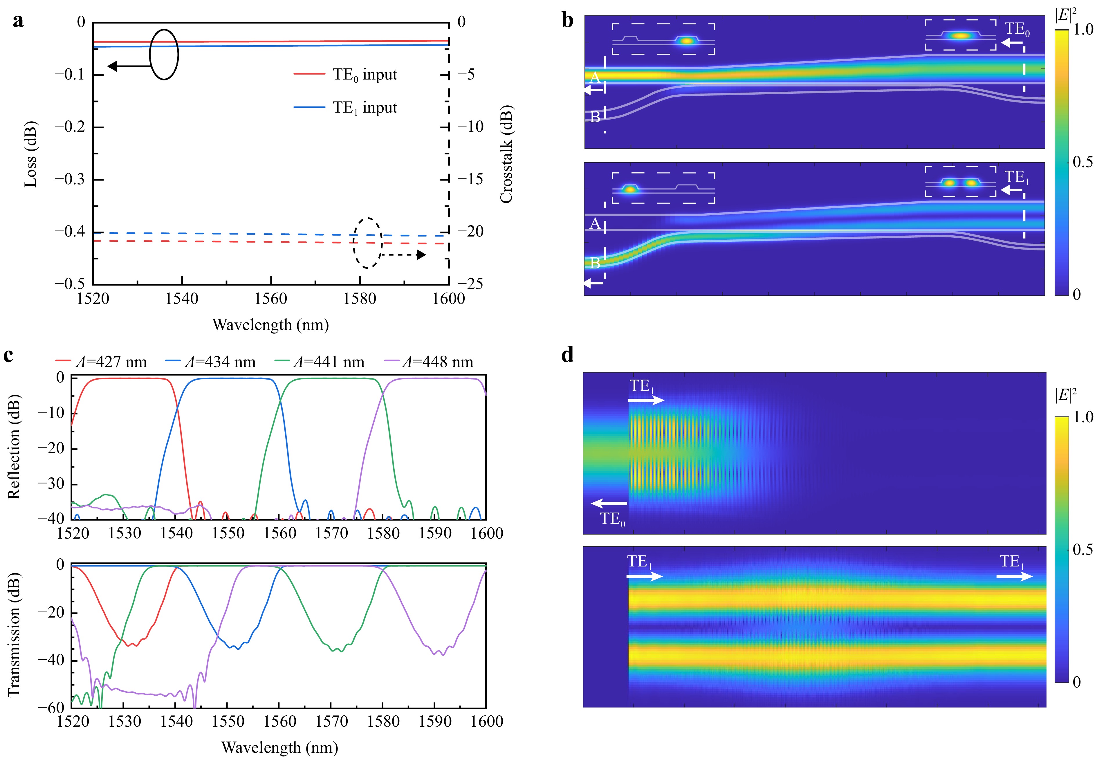
Fig. 2 Calculated results for the dual-core mode (de)multiplexer a, b and MWGs for the WDM filter c and d. a Propagation loss and crosstalk of the mode (de)multiplexer. b Light propagation in a mode (de)multiplexer when the backward TE0 or TE1 mode is launched at the right port of waveguide A. Insets: eigenmodes at different cross sections. c TE1-TE0 reflection and TE1-TE1 transmission of the four MWGs with different grating period Λ. d Simulated light propagation in the MWG for channel #2 at wavelengths of 1551 nm (reflection) and 1571 nm (transmission).
The MWG has the effective waveguide width W of 2 μm, and Gaussian apodization is applied to the corrugation depth δ to realize a high sidelobe-suppression ratio (SLSR) and reduce the crosstalk between channels. Accordingly, δ = δ0exp[−b(i−N/2)2/N2], where δ0 is the maximum corrugation depth, b is the apodization index, N is the total number of the grating period, and i = 1, …, N. Here, the apodization index b was set to 10. The reflectivity and the bandwidth of MWG filters are mainly determined by N and δ, which are optimized to be 450 and 640 nm, respectively. The MWG periods Λ of the four channels were chosen as 427, 434, 441, and 448 nm according to the central wavelength requirements.
Fig. 2c, d shows the three-dimensional finite-difference time-domain (3D-FDTD) simulation results of the TE1-TE0 reflection (i.e., the mode conversion from the forward TE1 to the backward TE0 mode) and the forward transmission of the TE1 mode for the four designed MWGs individually when the TE1 mode is launched (forward). The corresponding central wavelengths of the four MWG filters are 1531, 1551, 1571, and 1591 nm. It can be seen that the TE1-TE0 reflectivity of the MWG is as high as 99.5% and finally the backward TE0 mode is then output with very low losses from waveguide A of the mode (de)multiplexer. Correspondingly the power coupled from the backward TE0 mode back to the input port (waveguide B) is negligible because the mode (de)multiplexer works well with very low crosstalk. In addition, the MWG reflection from the forward TE1 mode to the backward TE1 mode is less than –50 dB, as expected in theory, and thus little power is reflected back to the input port (waveguide B).
Fig. 2c shows that the 1-dB bandwidth is as large as 16.5 nm (which is very high with respect to the channel spacing of 20 nm), featuring low-loss box-like responses. Furthermore, the SLSR is theoretically better than 35 dB over a wide wavelength range. In the wavelength range shorter than the Bragg wavelength of the desired TE1-TE0 reflection, the TE1 mode can partially be coupled/reflected into the higher-order modes with lower effective indices, according to the coupled mode theory. For example, TE1-TE2 reflection occurs in the range of 1525–1545 nm for the MWG of channel #4, as exhibited in the transmission spectrum in Fig. 2c (purple line). Fortunately, the reflected higher-order mode is not supported in the following part and dissipates along the tapers and the mode (de)multiplexers, which thus has no effect on the channels at the left. The similar situation occurs when the TE0 mode is launched to the MWG. To ensure that the output TE0 mode of each channel passes through subsequent filters with low loss, the four MWGs are cascaded in an optimal sequence so that λ1 < λ2 < λ3 < λ4, where λ1 and λ4 are respectively the central wavelengths of the MWGs at the leftmost and the rightmost, as depicted in Fig. 1a. Fig. 2d presents the simulated light propagation of the input TE1 mode in the designed MWG with Λ = 434 nm (channel #2) when operated at wavelengths of 1551 and 1571 nm, respectively.
For the modulator based on a 2 × 2 FP cavity, as shown in Fig. 1b, a pair of MWGs is used as the input and output reflectors. A mode (de)multiplexer was incorporated to separate the light reflected from the FP cavity from the incident light. The G-S electrodes with separation d were placed symmetrically on both sides of the FP cavity. The refractive index of the LN is modulated by the Pockels effect when electrical signals are applied to the electrodes. Accordingly, resonance wavelength shifts and intensity modulation were achieved at the reflection port for lunched light with a fixed wavelength. Based on our previous work, the balance between the modulation bandwidth and efficiency for an FP-cavity modulator can be achieved by carefully designing the reflectivity of the MWGs and the cavity length. To avoid the metal absorption loss in the MWG area, δ0 = 600 nm and d = 5 μm were selected for the FP cavity. In theory, when the period number N for the MWG is set to 180, the estimated reflectivity is 0.85 and intrinsic grating loss is lower than 0.015 dB; Theoretically, the loss can be reduced by decreasing the corrugation depth and increasing the period number52,53. The length Lwg was set to 20 μm to form a ~100-μm-long equivalent modulation region.
-
The designed LNOI photonic chip constituting four-channel EO modulators was fabricated on an X-cut LNOI wafer (NANOLN) with a 400-nm-thick LiNbO3 layer and a 3-μm-thick buried oxide layer. Further details regarding the fabrication can be found in Materials and Methods. Fig. 3a displays an optical microscopy image of the fabricated LNOI photonic chip with four FP-cavity modulators and a four-channel WDM filter. Fig. 3b–e presents the scanning electron microscopy images for different apodization parts of the MWG, as well as the dual-core waveguide coupling region for the mode (de)multiplexer and its cross section, respectively. It is clear that the waveguide sidewalls were all smooth with the same angle. As shown in Fig. 3e, the etch depth of the 250-nm-width trench is approximately 180 nm, shallower than other open regions (with an etch depth of ~200 nm). This is because smaller feature size leads to a slower etch rate, which is the so-called lag effect54, existing commonly in the dry etching process for narrow trenches. The lag effect usually occurs with high aspect ratio (> 1) in other platforms such as silicon. In contrast, it should be noted that the aspect ratio is 0.8 only (< 1.0) in our experiment. This is probably because of the non-vertical sidewall (~30° relative to the vertical axis) of the LN waveguide. Thus, such a lag effect should be carefully considered for the device design.
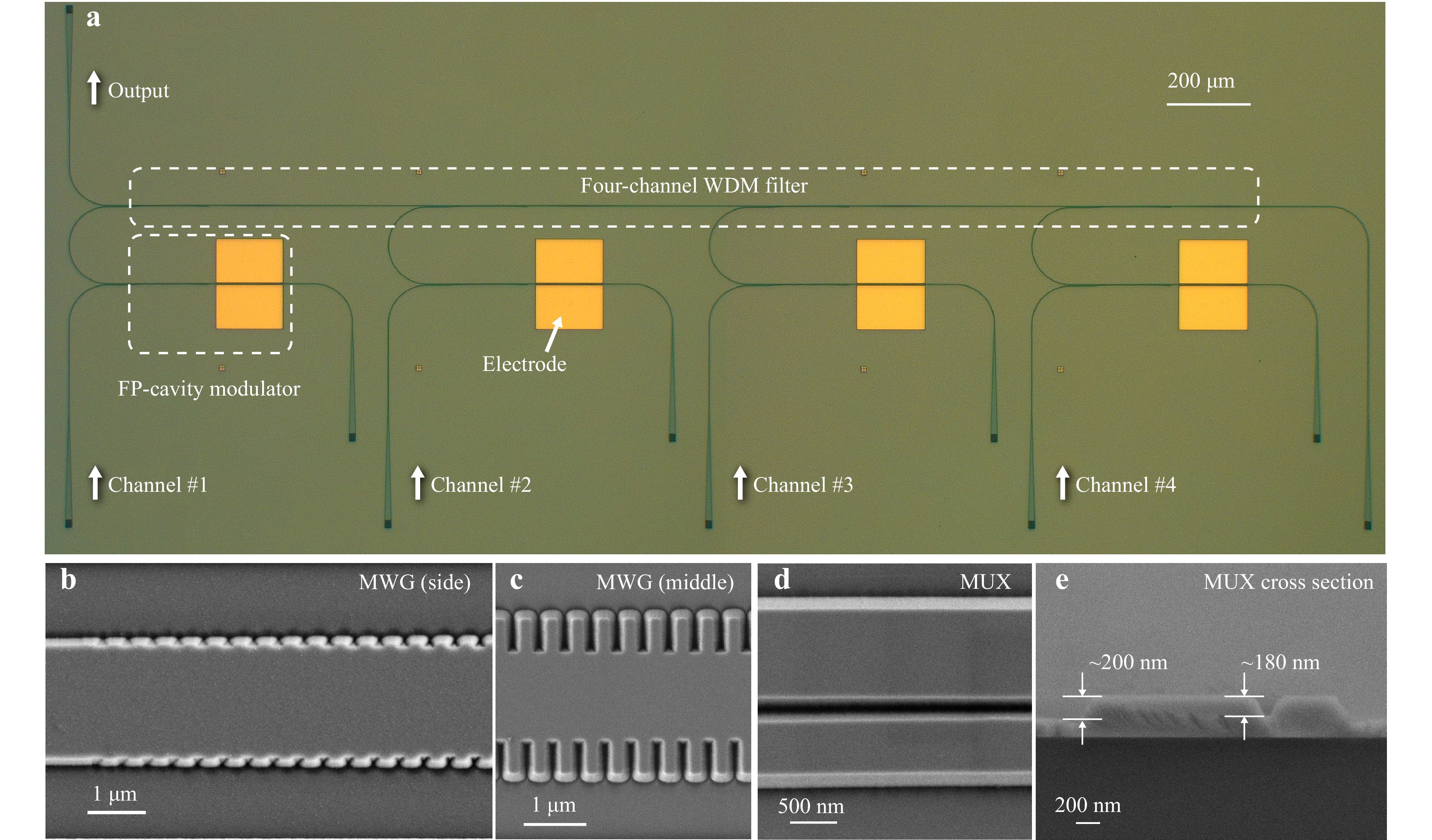
Fig. 3 a Optical microscopy image of the fabricated LNOI photonic chip comprising four EO modulators and a four-channel WDM filter. Scanning electron microscopy images of b, one side and c, the middle part of an MWG, d the dual-core taper of the mode (de)multiplexer, and e, the cross section of the mode (de)multiplexer.
The fabricated LNOI photonic chip was characterized using a setup including a broadband-amplified spontaneous-emission (ASE) light source and an optical spectrum analyzer (OSA). Fig. 4a presents the measured output spectra of the four-channel MWG-based WDM filter. The results were normalized to the transmission of a straight waveguide connected to two grating couplers on the same chip. For the fabricated WDM filter, the channel spacing is 20 nm (which agrees well with the design value), while the excess loss is < 0.8 dB and the channel crosstalk is less than –22 dB at the central wavelengths. More importantly, the WDM filter features box-like responses with a 1-dB bandwidth as large as 16 nm. Some ripples were observed at the edges of the channels. No ripples are observed from the simulation result (Fig. 2c) or the measurement transmission of a single MWG, indicating that ripples originated from the interference due to the reflections of the cascaded MWGs. Fortunately, these ripples do not have a notable negative impact on devices used in WDM systems. Fig. 4b exhibits the measured transmissions from the four input ports to the output port of the fabricated LNOI photonic chip. The measured transmissions were a combination of the transmissions of the FP-cavity modulator and MWG-based WDM filter. Consequently, several notches corresponded to the FP cavity resonance wavelengths, as observed from the measured transmission for each channel. The Q-factors of the FP cavities for four channels are approximately 5450, 6160, 6180 and 6450, the extinction ratios (ERs) are all greater than 20 dB, and the FSR of each cavity is approximately 7 nm, which is consistent with the design. Note that the cavity FSR can be increased, such as by decreasing the FP cavity length Lwg, or introducing a defect in the MWG to form a phase-shifted grating55. From Fig. 4b, the excess losses of Channels #1 and #4 are 0.4 and 0.8 dB respectively, indicating that the present WDM filter has an additional loss of ~0.15 dB per stage, and thus is possible to be scaled for more channels in the future. To demonstrate the EO property, a static electric field was applied to the modulators. From the measured resonance shift on voltage, a tuning slope of 9.6 pm/V could be obtained.
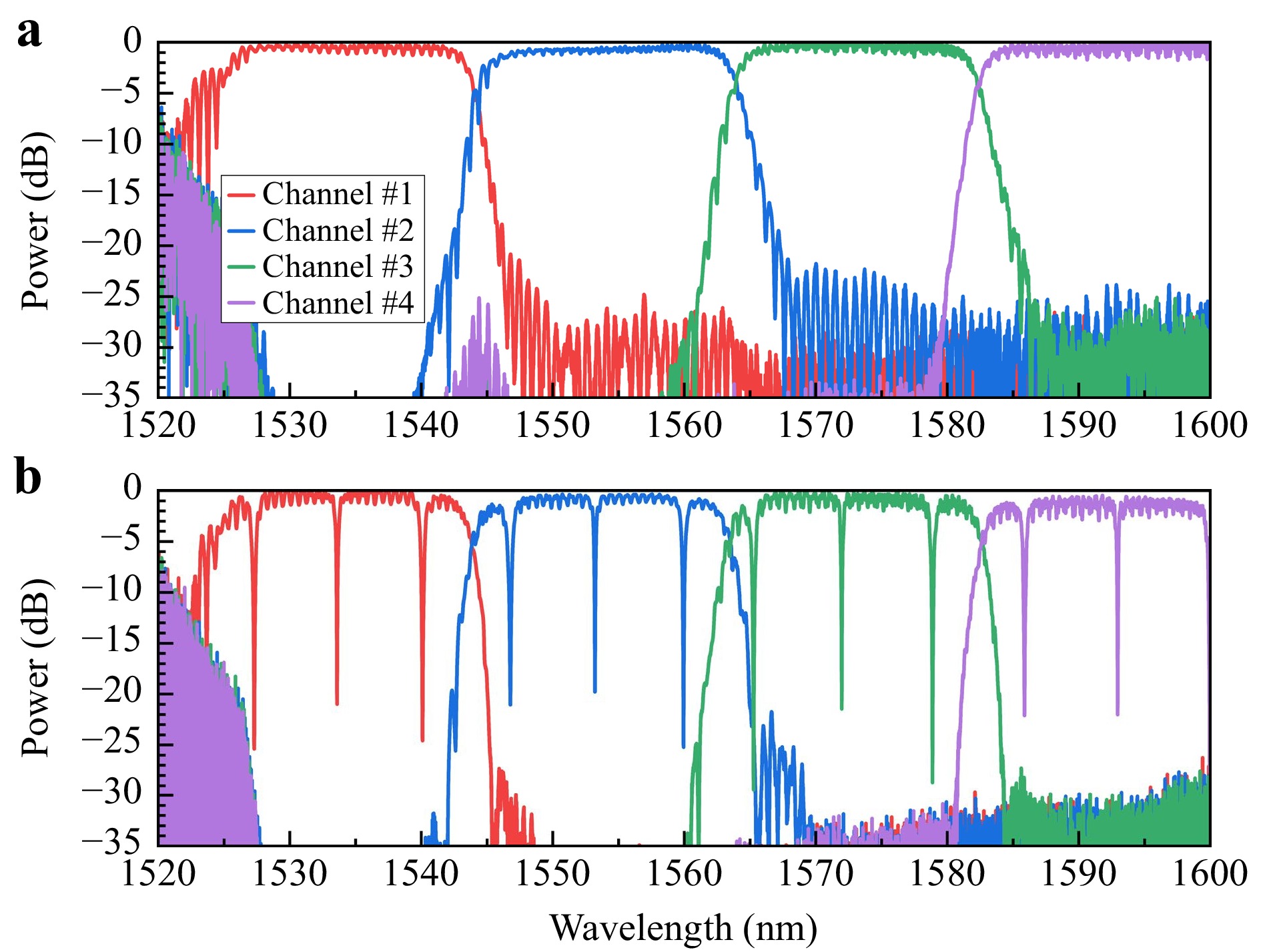
Fig. 4 a Measured transmissions of the fabricated four-channel WDM filter based on MWGs. b Measured transmissions from one of the four input ports to the output port of the fabricated LNOI photonic chip.
-
The fabricated LNOI photonic chip was characterized for high-speed data transmission. Further details regarding the experimental setup can be found in Materials and Methods. The modulation bandwidth limited by the photon lifetime in theory can be estimated as BW = f0/Q, where f0 is the resonant frequency and Q is the quality factor of a cavity. For the modulators of the four channels, the bandwidths are approximately 36, 31, 31, and 29 GHz, respectively, according to their measured Q factors. Adjusting the operation wavelength detuning to the resonance is helpful to further improve the 3-dB modulation bandwidth, as analyzed in our previous work28. Fig. 5 shows the measured eye diagrams for the four channels with 40/80 Gbps OOK signals and the 100 Gbps (50 GBaud) PAM4 signals. Limited by laboratory facilities, the experiments of data transmissions were run for each channel individually. As shown in Fig. 5a–d, all the channels perform similarly for the 40-Gbps OOK signals, featuring the dynamic ERs of 2.99, 3.11, 2.96, and 3.12 dB, respectively. For the eye diagrams of these four channels, there are slight differences due to the inconsistency of their optimal operating biases in the testing. The measured results for the 80-Gbps OOK signals are displayed in Fig. 5e–h. Owing to the limitations of the bandwidth and linear range of the radiofrequency (RF) amplifier, the voltage Vpp applied to the probe drops to 1.5 V and consequently, the signal is distorted. Meanwhile, the other electronic components such as the RF cables also greatly limit the experimental measurement of high-speed transmissions. By increasing the drive voltage and improving the bandwidth of the measurement system, high-quality OOK eye diagrams can be achieved at very high data rates. Alternatively, Fig. 5i–l presents the measured eye diagrams for the 100 Gbps PAM4 signals. The eyes are open for three channels (#1–#3), while the eye diagram for channel #4 is worse. This is owing to the low coupling efficiency of the grating couplers and the low gain coefficient of the erbium-doped fiber amplifier when operating at a long wavelength of approximately 1600 nm. Fortunately, broadband fiber-chip couplers (e.g., edge coupling56,57) for LNOI waveguides are available using the present fabrication technology. Consequently, the present transmitters are expected to work well with all four channels and enable a high total capacity of 4 × 100 Gbps. For each FP-cavity modulator in the present photonic chip, the capacitance is approximately 21.1 fF and the corresponding electrical energy consumption is estimated to be ~11.9 fJ/bit for the data transmitting up to 80 Gbps and beyond when operating with the bias of 1.5 Vpp. The link capacity can be further improved by introducing additional wavelength channels.
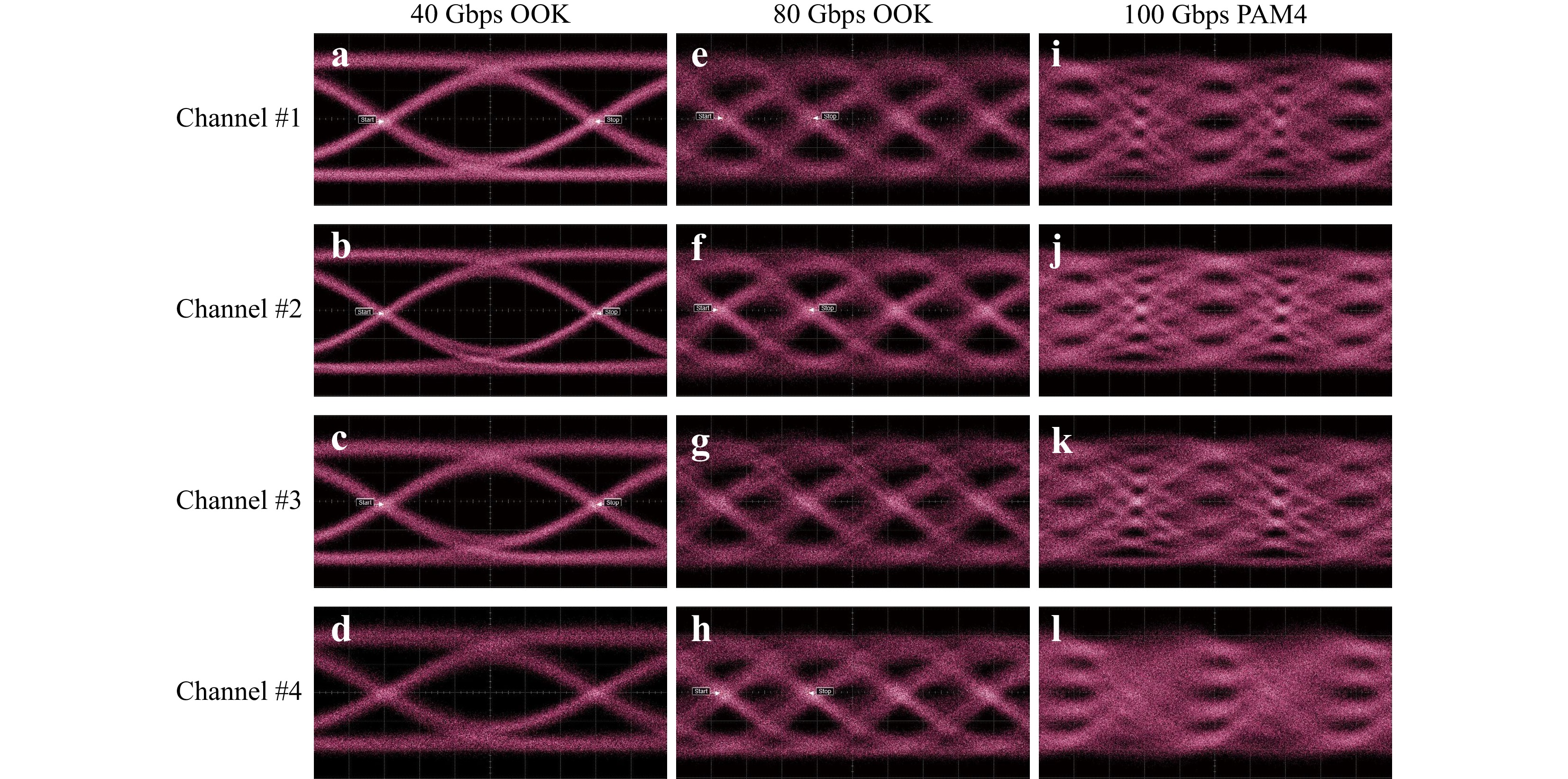
Fig. 5 Measured eye diagrams of each channel for a–d, 40-Gbps OOK signals, e–h, 80-Gbps OOK signals, and i–l, 100 Gbps PAM4 signals.
-
We proposed and demonstrated an ultracompact LNOI photonic chip to realize four-channel WDM transmitters by monolithically integrating four FP-cavity modulators and a four-channel WDM filter based on MWGs. The designed and fabricated WDM filters exhibited box-like responses with low excess losses (< 0.8 dB) and low crosstalk (better than −22 dB) for all channels. For the fabricated FP-cavity modulator of each channel, which had a Q-factor of approximately 6000, the extinction ratio was greater than 20 dB and the FSR was approximately 7 nm. All four channels demonstrated very low and uniform excess losses. The present photonic chip integrating four FP-cavity modulators and a four-channel WDM filter has a very compact footprint of 0.3 × 2.8 mm2, which is attractive for cases requiring even more WDM channels. The present LNOI photonic chip was further employed to realize high-capacity data transmission, and eye diagrams were demonstrated with 320-Gbps (4 × 80 Gbps) OOK signals and 400-Gbps (4 × 100 Gbps) PAM4-signals. Correspondingly, the power consumption is as low as 11.9 fJ/bit for each channel. The present photonic chip with an ultracompact footprint can be scaled for more channels and thus shows great potential for further realization of ultrahigh-capacity and energy-efficient WDM transmitters on LNOI in the future. In addition, the fabrication process can be improved by introducing SiO258, amorphous-Si59, or Cr60,61 hard masks. With an improved etching process, the propagation loss (mainly originating from the scattering loss at the sidewalls) can be reduced to a wafer scale58, which is very helpful for developing high-performance LNOI photonic integrated circuits and satisfying the growing demands for various applications.
-
Note that the popular fluorine-based reactive-ion etching method used for silicon or silicon nitride is not available for LN because of the redeposition of the solid byproduct lithium fluorine, which impedes further etching and increases the sidewall roughness. Instead, a popular approach for LN dry etching involves the use of Ar gas. For such a pure physical etching process, the challenge is to realize vertical and smooth sidewalls using an etching recipe with high selectivity. Therefore, etching parameters should be carefully optimized. In the etching process, Ar plasma may damage the mask and roughen the sidewalls, particularly in the deep-etching case. Fortunately, the etching selectivity can be improved by decreasing the power and gas flow rate45 when using electron beam resists such as HSQ14,46, ZEP25, and ma-N240322,27 for the mask.
The fabrication of the LNOI photonic device is described in detail as follows. First, the waveguide structure patterns were defined via a single step of electron-beam lithography (EBL) in a maN-2403 resist with a thickness of approximately 350 nm. Second, the LN layer was etched with the depth of 200 nm through an optimized Ar-gas-based ICP process with an etch rate of ~30 nm/min. Cleaning of the chamber before etching is usually necessary. During the etching process, the chamber temperature continually rises. To avoid the mask being damaged by high temperature and ensure selectivity in this study, the temperature was set to 10 °C and He gas was fed under the sample for cooling. Finally, titanium/gold electrodes with thicknesses of 10/150 nm were deposited via a liftoff process.
-
In the high-speed data transmission experiment, a pseudo-random binary sequence electrical signal was generated using an arbitrary waveform generator connected to a clock source. The driver signal was fed to a linear RF amplifier (SHF S807 C) followed by a 6-dB attenuator to avoid reflection damage before being coupled to the GS pads via a 67-GHz RF probe. The actual peak-to-peak Vpp applied to the probe was approximately 1.8 V at the 40-Gbps data rate of the OOK signals. A tunable continuous-wave (CW) laser source near the resonant wavelength was fed into the input port of the corresponding channel. The modulated light was then multiplexed to the output port using a WDM filter. Finally, the transmitted signal was amplified through an erbium-doped fiber amplifier comprising an optical bandpass filter and collected by an electrical sampling oscilloscope.
-
This work was supported by the National Major Research and Development Program (No. 2018YFB2200200/2018YFB2200201), National Science Fund for Distinguished Young Scholars (61725503), National Natural Science Foundation of China (NSFC) (91950205, 61961146003, 92150302, 62105283, 62205286), Zhejiang Provincial Natural Science Foundation (LD19F050001), Zhejiang Provincial Major Research and Development Program (No. 2021C01199), Leading Innovative and Entrepreneur Team Introduction Program of Zhejiang (2021R01001), and the Fundamental Research Funds for the Central Universities. The authors thank the Westlake Center for Micro/Nano Fabrication for the partial facility support.
Ultra-compact lithium niobate photonic chip for high-capacity and energy-efficient wavelength-division-multiplexing transmitters
- Hongxuan Liu1,
- Bingcheng Pan1,
- Yishu Huang1,
- Jianghao He1,
- Ming Zhang1, 2,
- Zejie Yu1, 3, 4,
- Liu Liu1, 3, 4,
- Yaocheng Shi1, 2, 3, 4,
-
Daoxin Dai1, 2, 3, 4, *, ,

- Light: Advanced Manufacturing 4, Article number: 13 (2023)
- Received: 02 December 2022
- Revised: 04 May 2023
- Accepted: 05 May 2023 Published online: 29 May 2023
doi: https://doi.org/10.37188/lam.2023.013
Abstract: Recently, high-performance thin-film lithium niobate optical modulators have emerged that, together with advanced multiplexing technologies, are highly expected to satisfy the ever-growing demand for high-capacity optical interconnects utilizing multiple channels. Accordingly, in this study, a compact lithium-niobate-on-insulator (LNOI) photonic chip was adopted to establish four-channel wavelength-division-multiplexing (WDM) transmitters, comprising four optical modulators based on ultracompact 2 × 2 Fabry-Perot cavities and a four-channel WDM filter based on multimode waveguide gratings. The fabricated chip with four wavelength channels has a total footprint as compact as 0.3 × 2.8 mm2, and exhibits an excess loss of ~0.8 dB as well as low inter-channel crosstalk of < –22 dB. Using this LNOI photonic chip, high-capacity data transmissions of 320 Gbps (4 × 80 Gbps) on-off-keying signals and 400 Gbps (4 × 100 Gbps) four-level pulse amplitude signals were successfully realized with the ultra-low power consumption of 11.9 fJ/bit.
Research Summary
Lithium Niobate Photonic Chip: High-capacity and Energy-efficient Wavelength-division-multiplexing Transmitters
Ultra-fast modulation and wavelength-division-multiplexing are key points to expand capacity in optical interconnects. Modulators on lithium-niobate-on-insulator (LNOI) platform are able to achieve high-speed and low-loss electro-optic modulation. However, it is still challenging to realize on-chip multi-channel optical transmitter due to the anisotropy of LN and the large footprints. Daoxin Dai’s group from Zhejiang University in China now report an ultracompact LNOI photonic chip, comprising four optical modulators based on ultracompact 2×2 Fabry-Perot cavities and a four-channel WDM filter based on multimode waveguide gratings. The design avoids any waveguide bends in the key regions, resulting in small size, design flexibility, and scalability. The fabricated chip exhibits high-performance in both excess loss and data transmissions, showing great potential for further realization of ultrahigh-capacity and energy-efficient WDM optical interconnects and optical computing on LNOI.
Rights and permissions
Open Access This article is licensed under a Creative Commons Attribution 4.0 International License, which permits use, sharing, adaptation, distribution and reproduction in any medium or format, as long as you give appropriate credit to the original author(s) and the source, provide a link to the Creative Commons license, and indicate if changes were made. The images or other third party material in this article are included in the article′s Creative Commons license, unless indicated otherwise in a credit line to the material. If material is not included in the article′s Creative Commons license and your intended use is not permitted by statutory regulation or exceeds the permitted use, you will need to obtain permission directly from the copyright holder. To view a copy of this license, visit http://creativecommons.org/licenses/by/4.0/.

 DownLoad: