


-
As a structure composed of two-dimensional arrays of microscale lenses, micro-lens array (MLA) has attracted attentions of both the academia and industry, due to its distinctive optical properties and wide applications. Recently, MLA has gradually stepped into diverse application fields, such as the wave front sensing1,2, virtual reality/augmented reality display3,4, beam shaping5,6, micro/wide viewing angle imaging7, light-field camera8,9, optical communication10 and many other emerging applications11-15. Generally, commercially applicable MLAs are expected to have different aspheric surface to satisfy the various application requirement. However, by the traditional MLA fabrication approaches, such as the hot reflow16-18, ink-jet19-21 and self-assembly22-24, it is difficult to fabricate aspheric micro-lens array (AMLA) directly with a desired arrangement and profile, which determines AMLA’s optical performances. Meanwhile, the drawbacks, such as the debris induced by the top-down writing, difficulties in the topography controlling and the process complexity, hinder these methods from large-scale commercialization.
Recently, two photolithography methods have been reported for AMLA fabrication. One is based on the digital micro-mirror device (DMD), a three-dimensional (3D) lithography technology that digitizes the position and intensity of the illumination by accurately switching one million micro-mirrors at a high frequency25. The other one is based on the femtosecond-laser-induced two-photon polymerization (TPP), a 3D printing technology with a nanometer precision through the two-photon absorption26,27. These two technologies are introduced for AMLA fabrication due to the controllability of the fabricated 3D profiles25-27. However, both of them suffer from unavoidable drawbacks. The AMLA fabricated by DMD has a relatively high surface roughness beyond 1 μm, i.e., at the level of lens dimensions, which will reduce the quality of micron imaging. The TPP technology faces a challenge in the large-area fabrication of the AMLA, due to the low manufacturing efficiency. These drawbacks restrict the further development of these two typical methods for the AMLA fabrication.
To meet the industrial fabrication speed and area under the condition of ensuring the optical characteristics, a 7-bit direct laser writing lithography (DLWL) technology realized by the single beam exposure comes back into researchers’ vision28. Compared with the DMD based laser direct writing lithography with only dozens or hundreds of grayscale level exposure, micro-structures fabricated by the 7-bit DLWL still have similar dark grids. Therefore, extra processes are required to reduce the surface roughness, which change the fabricated morphologies. Owing to the beam exposure achieved by electrical modulation, the number of changes in current intensity can reach 4096, which induces the laser intensity control of each exposure can be as high as 12-bit grayscale levels. The increase of the vertical writing resolution means the fabricated devices have a smoother surface, eventually leading to a qualitative improvement in the optical performance of the fabricated optical micro-devices. Besides, the DLWL technology is featured with high-speed and large-area fabrication. Compared with other method, the large-area microstructures can be transferred to other materials without complex mould29. Therefore, fabricated products have a cost-effectiveness advantage. Low cost advantage enables lab products to enter the industrial production line, and can also greatly reduce the cost of some expensive products, such as endoscope, high-end rescue equipment. Thus, this technology can promote the development of many industries.
Herein, we demonstrate the fabrication and characterization of AMLA via the single beam exposure DLWL, which can satisfy the high requirement of optical performances. To control the profile, an optimization method was employed in our study to reduce the AMLA profile deviation from the desired one. Parallel and scattered light sources were used to test the different optical performances of the AMLA, and the results meet quite well with our design. Due to the high flexibility of our approach, AMLA with different filling factors and an off-axis AMLA can also be readily fabricated with the one-step photolithography. Finally, an auto-stereoscopic-display with flexible thin film has been prepared by using above technology, which exhibits a new way to provide flexible holographic display at low cost.
-
The DLWL system employed in this study is illustrated by Fig. 1a. An emission laser beam with 405 nm and 635 nm wavelengths is generated, and the greyscales in beam exposure reach 4096 due to the electrical modulation. Before exposure, a laser source with 635 nm wavelength is used to scan the photoresist surface for a focus calibration. The desired light intensity and numerical aperture can be adjusted by an attenuator and an aperture diaphragm in compact optical system. Then, the emission laser beam is focused into a light spot on the photoresist via a condenser (100 × objective) to complete the exposure. To ensure the exposure speed, the moving scan axis under the photoresist is driven by an air bearing. To remain the fabrication accuracy, the whole compact optical system is drived by a high-accuracy linear bearing. The control of the linear bearing and air bearing are realized by programmable logic controller. The grayscale-typed photoresist is sensitive to the exposure power. With different exposure powers, the exposed depths of the photoresist are different. Therefore, by adjusting the exposure power during the exposure process, a 3D structure with a desired morphology can be obtained. Simultaneously, the better the linearity of the exposed material’s response to the intensity of the laser exposure, the closer the structure we prepared will be to the desired morphology. In this work, we chose photoresist AZ4562 as the material to fabricate the micro-lenses, which responds almost linearly to the exposure intensity. When the grayscale levels of DLWL are dozens or hundreds, there will be dark grids between the micro-structures prepared by a spot with different powers on the photoresist. The dark grids can be seen from the photoresist microstructures after development28. Due to the high resolution of 12-bit grayscale levels, it can realize a high writing resolution in the vertical direction. The high writing resolution induces the disappearance of dark grids between the microstructures. As a result, the AMLA fabricated by this photolithography technology does not require a post-processing to further reduce the surface roughness. In other words, an AMLA with desired profiles can be fabricated by the DLWL directly.
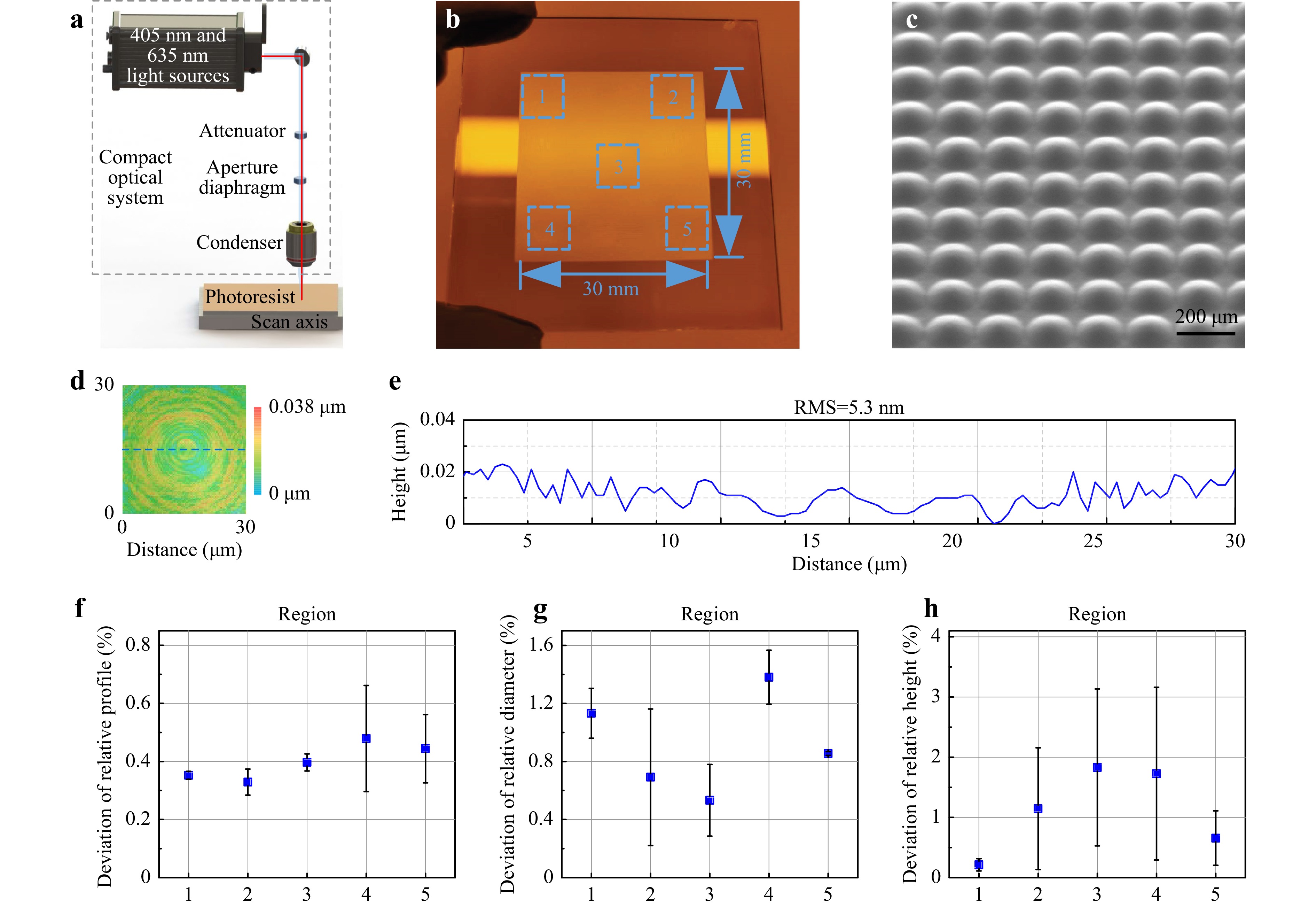
Fig. 1 Illustration of high-speed, large-area and high-precision AMLA fabrication. a Working principle of the direct laser writing lithography system for AMLA fabrication. b A photo of the fabricated AMLA with sizes of 30 × 30 mm2. c AMLA characterized via SEM (filling factor of 78%). d Surface height variation of a 30 × 30 μm2 area at the center of a micro-lens after excluding the experimental AMLA profile. e The line profile shown in d. f−h Relative diameter deviation, profile deviation and height deviation of the fabricated AMLA in different regions. The region numbers are denoted in b.
Based on the fabrication method mentioned above, as shown in Fig. 1b, we fabricated an AMLA with an area of 30 × 30 mm2 within 8 h 36 min, which means the writing speed exceeds 100 mm2/h. This preparation speed of the AMLA fully meets the requirement of industrialized mass production. Meanwhile, the AMLA observed via SEM demonstrates the fabricated AMLA possesses excellent morphologies and array property, and the surface is pretty smooth (Fig. 1c). Surface roughness, as a key parameter affecting the performance of the AMLA, is one of the most important parameters to evaluate the fabrication quality. To characterize the surface roughness, a single micro-lens was measured by a confocal microscopy (KEYENCE, VK-X3000), with a 30 × 30 μm2 field of view (FOV). The result shows that the surface height variation of a 30 × 30 μm2 area at the center of a micro-lens after excluding the AMLA profile (Fig. 1d). As shown in Fig. 1e, the corresponding root mean square (RMS) of the center is 5.3 nm, which indicates the sub 6 nm surface roughness of the AMLA. This surface roughness completely satisfies the requirements of the MLA based optical element30,31. Dark grids, a structure that significantly deteriorates the optical properties of MLA, would exist between pixels for the MLA fabricated by DMD31. Since the grayscale via DLWL reaches 12-bit, there is no grid between the spot tracks. The measurement results mentioned above verify that, the AMLA fabricated by the DLWL can realize a smooth surface without any post-processing, such as thermal reflow or plasma polish.
To test the uniformity and profile accuracy of the AMLA, five regions shown in Fig. 1b were chosen, with randomly selected single micro-lenses from each region to be characterized. Fig. 1f−h describes the profile deviation, relative diameter deviation and height deviation of the AMLA in these five regions, while the x-axis values corresponds to the region numbers shown in Fig. 1b. The profile deviation and relative diameter deviation of the micro-lenses are both below 2%, and the relative height deviation is below 3.5%. Besides, the uniformity of micro-lenses in each region is measured. The MLA was divided into 25 regions, as shown in Figure S1, and the standard deviation of 25 micro-lenses from these regions were measured. The results show that their standard deviations are 0.09, 0.41, and 1.32, respectively. The low deviation in profile, height and diameter indicates the high-quality fabrication of a large-area AMLA by the DLWL technology. The low value of standard deviation suggests a good uniformity in the fabricated micro-lenses.
-
A DLWL system can achieve a linear power output with 12-bit grayscales in the exposure process. To match the 12-bit grayscales of the linear power output, a 12-bit grayscale bitmap of the AMLA was designed. Here, as an example, the AMLA was designed with a filling factor of 78%, focal length of 688 μm at the wavelength of 450 nm, diameter of 160 μm for each single lens. The corresponding maximum sagittal height is as high as 10.38 μm and accurate profile control is necessary to guarantee the optical performance of the AMLA.
Here, a 3D Optical Proximity Correction (OPC) was proposed to realize high fidelity of AMLA. As a resolution enhancement technique (RET) in optical lithography, OPC combines the optical model to find the exposure dose inversely, with the goal of minimizing lithographic patterns and target patterns32-36.
In numerical models of lithography, scattering and cavity formation are usually ignored, and it is assumed that the light spot at the focal plane is a Gaussian distribution, the beam profile is approximately constant in the photoresist, and the optical properties of the photoresist are differentiable functions of the exposure state37-39. Therefore, the lithographic imaging process can be approximated as two operations: the convolution of the beam profile and the exposure position, and the resist effect can be described by the sigmoid function.
The imaging process of the numerical model is shown in Fig. 2a. Where B(x, y) is gaussian spot, E(x, y) is exposure distribution sampled by structure, and aerial pattern I(x, y) can be obtained through convolution operation39:
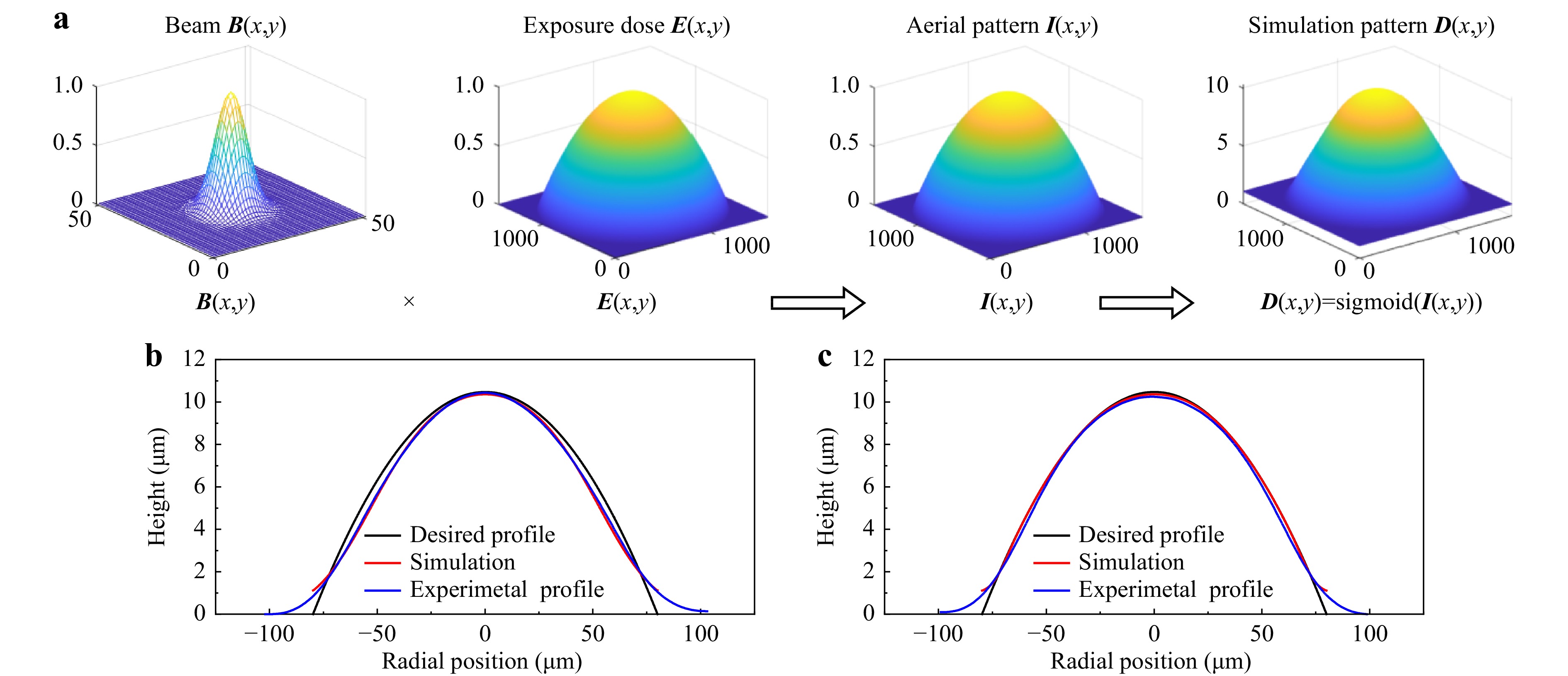
Fig. 2 Simplified simulation process of the numerical model. a In this imaging example, B(x, y) is the gaussian beam, E(x, y) is the exposure dose sampled by structure. The aerial pattern I(x, y) convolving B(x, y) and E(x, y). Finally, the resist effect is described by the differentiable sigmoid function, and the simulation pattern D(x, y) is approximated by Sigmoid (I(x, y)). b, c Schematic illustration of the AMLA profile b before and c after OPC, where black, red and blue lines represent target profile, simulation profile and experimental profile of AMLA respectively.
$$ {\boldsymbol I}(x,y)={\boldsymbol E}(x,y)*{\boldsymbol B}(x,y) $$ Then the simulation pattern D(x, y) can be calculated by resist effect:
$$ {\boldsymbol D}(x,y)=Sigmoid\left({\boldsymbol I}\right(x,y\left)\right) $$ where
$ Sigmoid\left(x\right)={\left[1+{\mathrm{e}}^{-\mathrm{a}(\mathrm{x}-{\mathrm{t}}_{\mathrm{r}})}\right]}^{-1} $ is the sigmoid function, with a and tr are calculated from the measured data.Given a desired pattern Dt, the object of OPC is to find the optimal exposure dose Eopt, which minimizes the pattern error between simulation pattern D and desired pattern Dt, and transformed into convex optimization problem:
$$ {{\boldsymbol E}}_{\mathit{o}\mathit{p}\mathit{t}}=argmin\mathrm{\epsilon }\left\{{||{\boldsymbol D}(E,B)-{\mathit{D}}_{{\boldsymbol t}}||}_{2}^{2}\right\} $$ Combining with trigonometric functions to constrain E(x, y), OPC can be transformed into an unconstrained optimization problem:
$$ \begin{array}{c}minimize\;{\boldsymbol F}={||{\boldsymbol D}(E,B)-{{\boldsymbol D}}_{{\boldsymbol t}}||}_{2}^{2}\\ s.t.\;\;{\boldsymbol E}\left(x,y\right)=\left(1+\mathrm{cos}\omega \right)/2\end{array} $$ where F is the cost function computed by the square of l2 norm
$ {||\text{∙}||}_{\text{2}}^{\text{2}} $ , which describe the sum of the errors between simulation pattern D(x) and desired pattern Dt at all pixels, with the name of pattern error (PE) in computational lithography.With the gradient of F with respect to
$ \mathrm{\omega } $ is36:$$ \begin{aligned}\boldsymbol\partial {\boldsymbol F}/\boldsymbol\partial {\boldsymbol\omega }=&\displaystyle\sum\limits _{x=1}^{{N}_{x}}\sum _{y=1}^{{N}_{y}}\left(\right({\boldsymbol D}(x,y)-{{\boldsymbol D}}_{{\boldsymbol t}}(x,y))\times \partial {\boldsymbol D}/\partial {\boldsymbol\omega })\\ =&a\sum _{x=1}^{{N}_{x}}\sum _{y=1}^{{N}_{y}}sin\omega \cdot\left(B*{d}_{1}\right)\end{aligned} $$ In which, * and · are convolution operation and entry by-entry multiplication operation, respectively, and
$ {d}_{1}=({\boldsymbol D}-{{\boldsymbol D}}_{{\boldsymbol t}})\times {\boldsymbol D}\times ({\bf 1}-{\boldsymbol D}) $ .Thus, the update of variables based on steepest gradient descent (SGD) can be expressed as:
$$ {\boldsymbol\omega }={\boldsymbol\omega }-{\boldsymbol s}\cdot \boldsymbol\partial {\boldsymbol F}/\boldsymbol\partial {\boldsymbol\omega } $$ with s = 0.01 is the step-size of optimization.
Fig. 2b compares the desired profile, simulation profile and experimental profile of AMLA before OPC, and Fig. 2b compares the desired profile, simulation profile and experimental profile of AMLA after OPC. Notably, simulated PE decreased from 326900 in (b) to 198000 in (c) with 20000 iterations. Due to the analytical ability of the numerical model to the lithography process, the simulation results are consisted with the experiment results. Combined with the powerful inversion ability of OPC, we can continuously optimize the exposure distribution through simulation, which enables the AMLA morphology to be close to desired profile.
To numerically quantify the deviation level between the experimental and desired profiles, we introduce the relative profile deviation P which can be written as
$$ P=\sqrt{\frac{{\displaystyle\sum }_{i=1}^{n}\left(\dfrac{{y}_{e}\left({x}_{i}\right)}{{y}_{d}\left({x}_{i}\right)}-1\right)}{n}} , $$ where yd is the height value of the desired AMLA profile, ye is the height value of the experimental AMLA profile, and xi is the radial position in the region of desired profile. Here, the value of n is set to be 10, and xi is uniformly distributed over the desired region. The morphology accuracy can be further improved with a optimization time, although the deviation reduction with the interation (Fig. 2d). AMLA profile deviation can be reduced by increasing the optimization numbers, but meanwhile the optimization effect decreases with the increasing of the optimization numbers. After the 20000 OPC iteration, the relative profile deviation decreases successfully to be 0.28%, and this is a satisfactory value compared with the profile deviation of a micro-lens fabricated by the TPP technology40-42. The experimental morphology highly similar to the desired one induces excellent optical properties. An experiment shows the focal length is about 700 μm, which is very closed to desired value.
-
The fabricated AMLA has a low deviation from the desired profile, which aims to acquire the desired optical properties according to the design and simulation. Therefore, we mainly test two optical properties of the AMLA, i.e., imaging and light focusing quality. Two experimental setups have been built up to characterize the optical properties of AMLA, as shown in Fig. 3a, b. In Fig. 3a, a diffuse light source is placed below the AMLA to realize the imaging of the micro “F” pattern array. A charge coupled device (CCD) camera is used to observe the micro “F” pattern array amplified by a 20× objective lens. The demagnification of the “F” pattern array by the AMLA is shown in Fig. 3c. The observed micro “F” pattern has a clear margin, and the inset image shows a good intensity uniformity of the micro “F” patterns in the array compared with MLAs fabricated by other high speed manufacturing method43. This demonstrates that our method completes the high-speed and large-area fabrication of MLA without affecting the fabrication quality. In Fig. 3b, a parallel light source is employed to characterize the light focusing performance of the AMLA. Fig. 3d shows focal spot arrays formed by the parallel light with the wavelengths of 450 nm, 520 nm and 635 nm, respectively. The inset images in Fig. 3e depict the experimental results of the focal spot intensity distribution in the focal plane. To fit for the CCD working range, an attenuator is used to weaken the light intensity for a better observation. The experimental line intensity profiles of the focal spot are compared with the simulated line intensity profiles of the focal spot, with the wavelengths of 450 nm, 520 nm and 635 nm, as shown in Fig. 3e. For all wavelengths, the simulation and experiment show good agreement in the range of the focal spot radius (The lateral distance from the central peak to the first lowest point in the intensity distribution). Although MLAs fabricated by other methods can also complete the beam convergence, it is difficult to achieve the desired intensity distribution. This proves that AMLA fabricated by our preparation method is highly controllable, which can produce MLAs with desired light intensity distribution17,44,45. In the experiments, there are some ring-shaped halos around the focus spot, which could be induced by surface roughness, but the intensities of ring-shaped halo are much lower than the planar diffractive-type MLA46. This AMLA with a good focal spot intensity has a high sensitivity to the laser wavelength, which may be preferred in many potential applications.
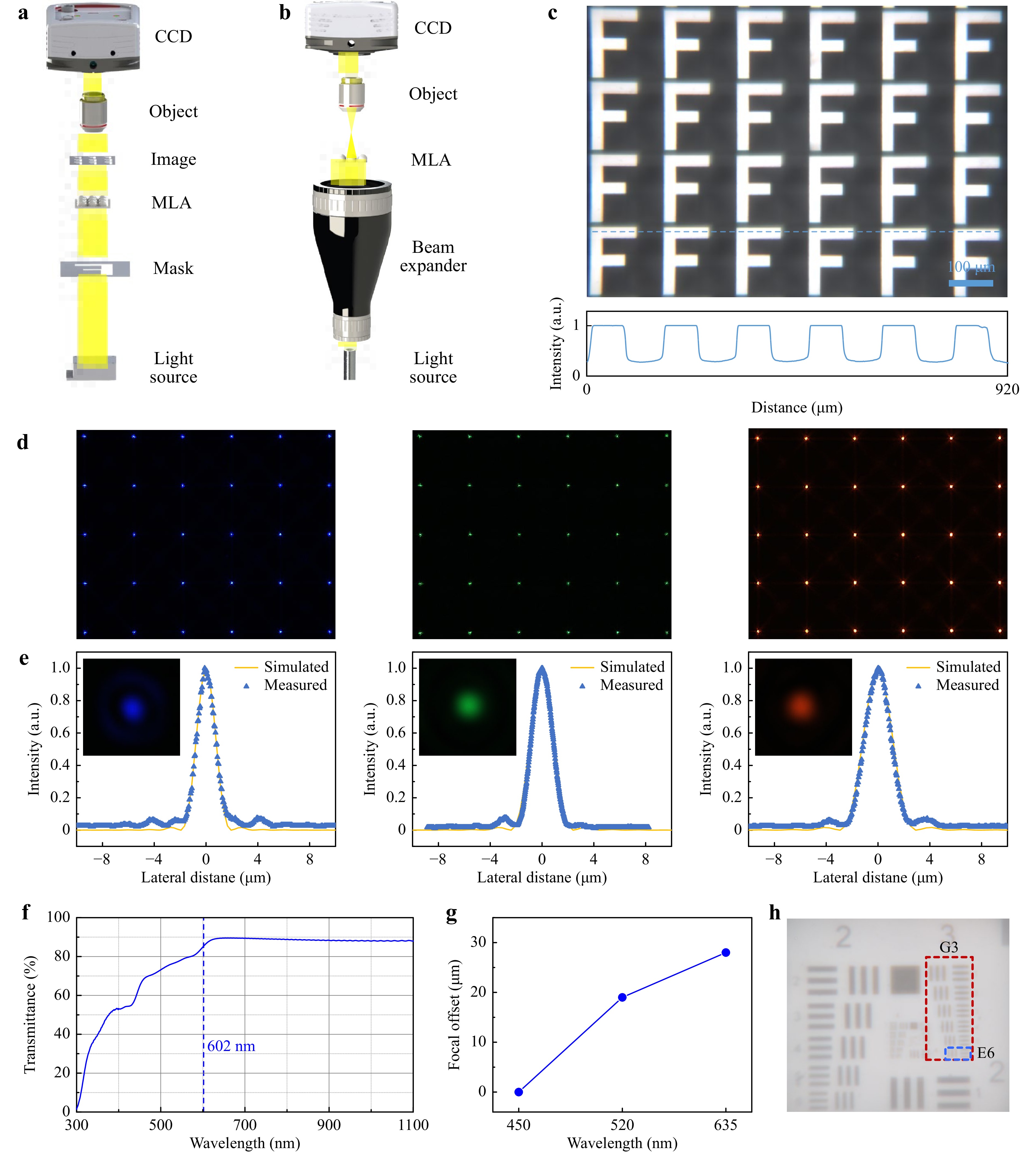
Fig. 3 Optical performance of the fabricated AMLA. a, b Optical setup for the AMLA imaging and beam focusing performance tests. c The image of “F” letters array formed by the AMLA. Inset image shows the line intensity profiles of the “F” letters array, and the blue line is shown in Figure 3c. d Experimentally captured focused spots with the wavelengths of 450 nm, 520 nm and 635 nm, respectively. e Comparison of simulated line intensity profiles of the focal spots with experimentally captured ones with the wavelengths of 450 nm, 520 nm and 635 nm, respectively. The inset images depict experimental results of the intensity distribution of a focus spot in the focal plane. f Transmittance of the AMLA in a wavelength range from 300 nm to 1100 nm. g Measured AMLA focus offset with the operating wavelength of 450 nm, 520 nm and 635 nm, respectively. h A standard USAF1951 resolution target imaged by the AMLA.
Next, we measured the transmittance, chromatic aberration and resolution of the fabricated AMLA. Fig. 3f depicts the measured transmittance of the AMLA in a wavelength range from the 300 nm to 1100 nm. In the wavelength range between 300 nm and 602 nm, the transmittances of the AMLA made of AZ4562 resist on the 1 mm thick glass is lower than 85%. However, the transmittances of the AMLA in the range from 602 nm to 1100 nm are up to 85%, indicating a high transmittance in the shortwave-near infrared range. When transferring the patterns on the AZ4562 resist to polymathic methacrylate, the high transmittance in the shortwave-near infrared range can also be expected due to the similar optical properties of the two materials47. To increase the transmittance, the pattern can be transferred to other materials, such as PDMS. Figure S2 shows the depend of transmittances on PDMS MLA diameters. It indicates that MLAs with different diameters have different transmittances. Fig. 3g describes the measured AMLA focus offset of 450 nm, 520 nm and 635 nm. With the material refractive index of 1.51, the maximum offset is lower than 30 μm, which is relatively low compared with the focal offset reported in other researches48. This can be attributed to the precise profile control and the low material dispersion when compared with a diffractive MLA.
A low surface roughness of the AMLA would contribute to a high imaging resolution. The resolution test system is the same system as the AMLA imaging performance test, just replacing the “F” pattern mask with a standard positive USAF1951 resolution test chart (Daheng Corp., GCG-0206). The test chart contains 6 groups of patterns from +2 group to +7 group, and each group possesses 6 elements. The line width in element 6 of the group 3 (G3) is 70.17 μm, and its imaging pattern via AMLA can be observed clearly in the pattern marked by the blue dotted line shown in Fig. 3h. The demagnification of the imaging system used in Fig. 3h is 20.66, so the minimum resolution of the AMLA reaches 3.39 μm, which is very close to the reported MLA resolution with the surface roughness of 1 nm49. This demonstrates that the AMLA fabricated by the DLWL technology is able to realize a high-resolution imaging without any post processing.
-
Compared to the traditional MLA fabrication methods, another benefit of this photolithography technology is the high flexibility in design50, which can significantly improve the performance of many functional devices based on MLA, such as laser beam shaper and wave-front sensor51. For example, to realize a freeform beam shaper, the micro-lenses inside a MLA should be aligned unregularly (i.e., the focused spot arrays are randomly distributed), which requires a complex greyscale mask for other approaches51. Using the laser direct writing lithography technology with a high degree of manufacturing freedom, we can directly fabricate an off-axis MLA to generate unregular spot arrays without the requirement of a complex greyscale mask. As an example, we designed an off-axis MLA composed of two types of off-axis micro-lenses, A and B, and each row has different axis directions compared with the neighbored rows, as shown in Fig. 4a. Fig. 4b shows the 3D morphology of the off-axis MLA, and the off-axis MLA was characterized via the SEM, as shown in Fig. 4d. We can observe that the highest point of the micro-lens is not located in the center, so although the MLA is a rectangular array, the arrangement of the focus is unregularly (Fig. 4c). In the real application, more complex beam shaping can be formed according to the practical requirements, without complicating the fabrication of MLA. Furthermore, according to the design to satisfy different application requirements, we can also fabricate the MLA with different heights, diameters and curvatures, and transfer the pattern of the fabricated MLA to other flexible transparent material, such as PDMS. Fig. 4e, f shows the transferred PDMS-based MLAs arranged in a rectangular array with a filling factor of 90.7% and a full-packed array with a filling factor of 100%, which has shown their high-fidelity and high-uniformity with less distortion. Meanwhile, this pattern transfer method suggests a low-cost way for mass fabrication of flexible transparent MLA.
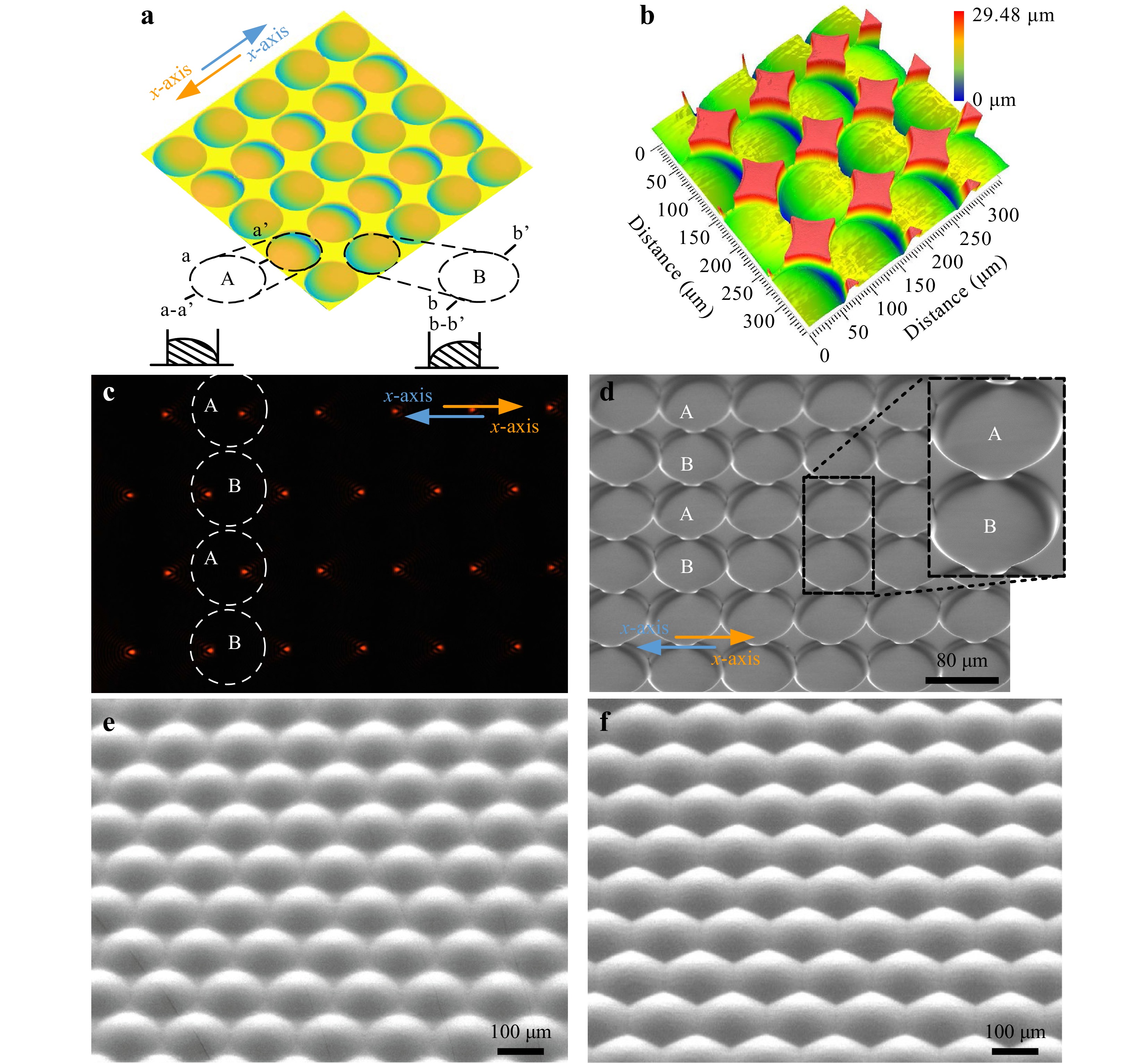
Fig. 4 Characterization of an off-axis MLA and MLAs with different filling factors. a Schematic diagram of an off-axis MLA. b Three-dimensional topography of a fabricated off-axis MLA. c Experimentally captured focused spot arrays with the operating wavelength of 635 nm. d Off-axis MLA characterized via the SEM. e, f SEM photos in partial views of the MLAs with filling factors of 90.7% and 100%.
-
Autostereoscopic-display technology in holography has been widely used in biomedicine52, data visualization53 and other fields54,55. Aiming to achieve large-area autostereoscopic-display at low cost has always been a research hotspot in industry and academia56. Here, we used the proposed fabrication technology to prepare the transparent AMLA, then the AMLA was bonded on the patterned substrate. Via an accurate morphology control of the prepared micro-lens, the focus spots of the fabricated micro-lens can be well located in area of the bonding pattern, as shown in Figure S3. In this way, the micro-lens’ field of view enables an autostereoscopic-display effect of the patterns on the substrate. Video SV1 and video SV2 in the supplementary material exhibit the described autostereoscopic-display effect. In the practice, large AMLAs would be fabricated to satisfy various application requirements. This technology provides a new way to fabricate flexible holographic display at low cost.
-
In addition to the DLWL method based on single beam exposure, TPP and DMD are currently two mainstream 3D lithography solutions for the AMLA fabrication. The two-photon lithography technology can fabricate 3D structure with the precision at the nanoscale. A 3D structure fabricated by the TPP technology is based on the principle of a two-photon principle. The two-photon phenomenon only occurs in the focus of laser beam. The focus at the nanoscale makes the structural accuracy at the nanometer level. This also gives it a high degree of manufacturing freedom. Meanwhile, the surface roughness is very smooth due to the motion platform at nanoscale. The fabrication speed of micro-lens based on the DMD technology is very fast. This is because it has millions of micro-mirrors to fabricate the microstructures at the same time. Although the two solutions have their own advantages in fabrication accuracy and speed, they each have certain shortcomings. Some work has been done by researchers to improve the related problems. Table 1 compares the characteristics and fabrication parameters of AMLA. The average error of 12-bit DLWD is close to 300 nm, which is smaller than some TPP technology. Meanwhile, the profile deviation is also very close to the fabrication limitation of TPP technology. Similarly, roughness has approached the fabrication limitation of 3D lithography technology. In terms of fabrication speed and area, the processing method of DLWD has significant advantages compared with TPP technology. TPP technology realizes the fabrication of AMLA through the assembly of a large number of laser-induced polymerized voxels with nanoscale. From the preparation perspective of 3D microscale structures, TPP technology uses 0D nanomaterials to build 3D microscale structures. For the DLWL technology, the upper and lower areas of the focused beam participate to the exposure of photoresist. Although more participation exposure areas would sacrifice certain precision, the exposed area is greatly increased without influencing the fabrication freedom. The increased exposure volume makes it easy to prepare large area microstructures. In other words, DLWL technology is employed 1D light beam to carve 3D microscale structures. This difference in terms of fabrication mechanism decides the higher fabrication speed of AMLA fabricated by DLWL technology. In order to solve the roughness problem of the AMLA prepared by DMD, researchers usually apply additional processing to the AMLA, such as reflow59 and oscillation49. Our processing method without additional processing also highlights our advantages of low-cost and simple processing.
Table 1. A summary of AMLA fabrication based on 3D lithography
-
In summary, we report a low-cost, high-precision, large-area and high-speed fabrication technology for AMLA based on the 12-bit direct laser writing lithography. We show the AMLA with dimensions of 30 × 30 mm2 can be fabricated within 8 h 36 min, corresponding to a high-speed writing exceeding 100 mm2/h. Meanwhile, the profile of fabricated AMLA was optimized successfully via a three-dimensional optical proximity correction (relative profile deviation down to 0.28%) and surface roughness was sub 6 nm in average. Because of the precise fabrication technology, the fabricated AMLA exhibited good optical performance in terms of imaging and light focusing. In particular, our approach shows good flexibility in MLA design, e.g., arbitrary off-axis MLA can be fabricated within only one-step lithography, which has showcased their precise profile control and high performance in beam focusing. Additionally, the transferred PDMS-based MLAs with different filling factors (90.7% and 100%) based on MLA master mould fabricated via DLWL suggest a feasible technology of the low-cost AMLA fabrication. Combined with the proposed fabrication technology, an autostereoscopic-display thin film is fabricated, which exhibit excellent 3D display performance. The proposed AMLA fabrication method based on the direct laser writing lithography can not only reduce the difficulty of preparing complex morphology MLAs, but also be very suitable for industrial production. This may greatly reduce the preparation cost of devices composed of micro-lens, such as endoscopes, infrared detectors, holographic displays, optical couplers, etc. Therefore, it would have big impact on the medical treatment, rescue, optical communication, military and many other related fields.
-
Optical setup: The main components of the optical characteristic measurement system of MLA are composed of two objective lenses (Daheng, GCO-2107; Daheng, GCO-2106), 4 light sources (Thorlab, CPS450; Thorlab, CPS520; Thorlab, CPS635; Lemons, KM-FL2929) and a charge coupled device (CCD) (Daheng, MER-2000-19U3C-L). Adjustment of the object distance and the image distance are realized by two three-dimensional motion platforms (Daheng, GCM-901602M).
AMLA design and fabrication: AMLAs were designed and numerically simulated with the commercial optical design software ZEMAX, which can focus incident light into nearly diffraction-limited spots. The simulated line intensity profiles of spots were acquired by ZEMAX. The photoresist (AZ4562) was prepared on a 1 mm thick glass by using the spin coating method. The spin coating includes two processes. The speed of the first process was 300 rpm/s, and the speed of the second process was 750 rpm/s. The photoresist on the glass was relaxed for 20 min. Next, we baked the photoresist with 90 °C for 25 min. After 1 min relaxation for cooling the photoresist, the photoresist was put into the DLWL device (4PICO, Pico Master 100). In the lithography process, the lithography spot was 550 nm, the steps were 250 nm, the speed was 200 mm/s, and the exposure intensity was 532 mj/cm2. Finally, the photoresist after the exposure was developed for 7 min 30 s.
Pattern transfer: Polydimethylsiloxane (PDMS) was drop-coated on an AMLA fabricated via DLWL. Then, the MLA coated with PDMS was delivered into an oven for 3 h, and the bake temperature was 90°. Next, the PDMS was stripped from the MLA. The PDMS was silanized for 60 s to acquire a template of the MLA. The PDMS was drop-coated on the template of the MLA. The template coated with PDMS was delivered into an oven with 90° for 3 h again. Finally, the PDMS was demoulded from the MLA template to acquire the PDMS MLA.
Characterization: Scanning electron microscope (SEM) images of the gold-sputtered AMLA were taken by the field-emission SEM (Tescan, brno, s.r.o.). In order to achieve a high-precision measurement, surface roughness was measured by a confocal microscopy (KEYENCE, VK-X3000). AMLA profile was measured by a white light interferometer (ZYGO, Nexview) to acquire more measured area. Transmittance of the AMLA was measured by a UV spectrophotometer (Lambda 365 UV-Vis spectrophotometer, Perkin Elmer).
-
Thanks for the SIMAX company support. This study was supported by the National Natural Science Foundation of China (U20A6004 and 91950110), and National Key R&D Program of China (2019YFB1704600).
High-speed, large-area and high-precision fabrication of aspheric micro-lens array based on 12-bit direct laser writing lithography
-
Shiyi Luan1,
 ,
, - Fei Peng2,
-
Guoxing Zheng3, 4, *, ,
,
-
Chengqun Gui2, *, ,
,
-
Yi Song2, *, ,
,
- Sheng Liu1, 2
- Light: Advanced Manufacturing 3, Article number: 47 (2022)
- Received: 09 May 2022
- Revised: 23 August 2022
- Accepted: 25 August 2022 Published online: 19 September 2022
doi: https://doi.org/10.37188/lam.2022.047
Abstract: Aspheric micro-lens array (AMLA), featured with low dispersion and diffraction-limited imaging quality, plays an important role in advanced optical imaging. Ideally, the fabrication of commercially applicable AMLAs should feature low cost, high precision, large area and high speed. However, these criteria have been achieved only partially with conventional fabrication process. Herein, we demonstrate the fabrication and characterization of AMLAs based on 12-bit direct laser writing lithography, which exhibits a high fabrication speed, large area, perfect lens shape control via a three-dimensional optical proximity correction and average surface roughness lower than 6 nm. In particular, the AMLAs can be flexibly designed with customized filling factor and arbitrary off-axis operation for each single micro-lens, and the proposed pattern transfer approach with polydimethylsiloxane (PDMS) suggests a low-cost way for mass manufacturing. An auto-stereoscopic-display flexible thin film with excellent display effect has been prepared by using above technology, which exhibits a new way to provide flexible auto-stereoscopic-display at low cost. In brief, the demonstrated fabrication of AMLAs based on direct laser writing lithography reduce the complexity of AMLA fabrication while significantly increasing their performance, suggesting a new route for high-quality three-dimentional optical manufacturing towards simplified fabrication process, high precision and large scale.
Research Summary
A large-area aspheric micro-lens array fabrication method
Large-area aspheric micro-lens array (AMLA) plays an important role in high-end optical sensing, communication and advanced optical imaging. Ideally, a commercially applicable AMLA should feature low-cost, high-precision, large-area and high-speed fabrication. However, these criteria have been achieved only partially with conventional fabrication process based on digital micro-mirror device and femtosecond-laser-induced two-photon polymerization. Professor Gui developed a 12-bit laser direct writing lithography technology with single beam exposure to fabricate AMLA, which can greatly improve both the writing speed and area without at the cost of reduced surface quality and poor shape profile. As an example, a large-area and high-precision AMLA was fabricated with dimensions as large as 30 × 30 mm2 and fabrication speed up to 100 mm2/hour. The relative profile deviation of a perfect micro-lens shape is compressed to be 0.28% via the proposed gradient convergence optimization method. The high-quality AMLA was experimentally demonstrated in terms of high-performance optical imaging, light focusing and focal length consistency. We believe that the delivered results, methodology and phenomenon can stimulate broad interest from readers in other fields such as advanced manufacturing, advanced display, and advanced laser fabrication etc.


Rights and permissions
Open Access This article is licensed under a Creative Commons Attribution 4.0 International License, which permits use, sharing, adaptation, distribution and reproduction in any medium or format, as long as you give appropriate credit to the original author(s) and the source, provide a link to the Creative Commons license, and indicate if changes were made. The images or other third party material in this article are included in the article′s Creative Commons license, unless indicated otherwise in a credit line to the material. If material is not included in the article′s Creative Commons license and your intended use is not permitted by statutory regulation or exceeds the permitted use, you will need to obtain permission directly from the copyright holder. To view a copy of this license, visit http://creativecommons.org/licenses/by/4.0/.

 DownLoad: