


-
Integrating miniaturized sensors with optical fibers is widely recognized as an important potential solution to instant and point-of-care medical diagnosis and on-site agricultural produce inspection. For example, it was listed as one of the key photonic solutions in face of the ageing society’s challenges by the 2018 Institute of Physics Report1. In general, devices integrated with optical fibers leverage the mature fiber-optic communication technologies and the flexible lightwave guiding of fibers2-6. Among them, sensing devices mounted on the flat end-facets of fibers make use of fiber’s convenient-and-rapid-operation capability to the fullest, for they can be directly dipped into minute amounts of biological and medical samples, or inserted into tissues and organs with minimal invasion to read molecular, optical and acoustic information3,5,7-13.
Encouraged by the success of surface plasmon resonance (SPR) sensing technology, numerous devices and fabrication methods have been proposed to integrate SPR upon optical fiber end-facets3,5-8,13-19. When employed in a free-space optics setup, SPR has shown high sensitivity to surface adsorption, making it a critical tool for biomolecular interaction analysis and biomolecular concentration quantification in modern life science and drug development20. However, the SPR and fiber end-facet integration endeavors have been hampered by their much lower performance compared with the free-space optics counterparts. There are two critical challenges. First, the fiber-guided lightwave has a certain range of transverse wave-vector distribution corresponding to the fiber’s numerical aperture, which prevents any uniformly periodic plasmonic structure from optimally interacting with the fiber-guided mode. This effect results in ultra-low quality factors (Q) or low coupling efficiencies, compared to the performance of the same SPR devices under free-space planewave illumination15,21. Second, it is difficult to apply the standard microfabrication techniques upon the tiny fiber end-facets. Although a variety of novel fabrication techniques were reported, including focused ion beam milling, nanoskiving, decal/template/direct transfer, interference/two-photon/through-fiber photolithography, nanoimprinting, nanosphere templating, self-assembly etc.2,3,5,6,12,15,22-28, there have been no successful reports on fabricating heterogeneous three-dimensional (3D) structures at the nanometer scale using a top-down approach, which further limits the development of high performance sensing devices on fiber end-facets.
In this work, we demonstrate a quasi-3D cavity on a single-mode fiber’s (SMF) end-facet with a high Q and a high coupling efficiency. As shown in Fig. 1, the device consists of a plasmonic crystal microcavity and a Fabry-Pérot etalon, which couple with each other through Fano resonance. The plasmonic cavity is used to accommodate the transverse wave-vector distribution of SMF, so as to achieve a high Q resonance; and the etalon is used to obtain a high coupling efficiency. Effectively, the Fano resonance’s phase shift moves the efficient F-P coupling point to the high-Q SPR wavelength. The resulting noise-equivalent limit-of-detection (LOD) is down to 1.9 × 10⁻⁷ refractive index unit (RIU), being much lower than any other fiber end-facet SPR sensors reported. In addition, we demonstrate a top-down fabrication method to transfer such a quasi-3D or multilayered SPR structure from a planar substrate onto the fiber end-facet. The transferring process is facilitated by the nanocap-slits in a noble metal film, of which the plasmonic cavity is comprised of, as shown in Fig. 1’s inset. By both having a low adhesion to the substrate (before the SPR device is peeled off and transferred) and facilitating surface plasmon polariton (SPP) tunneling through the metal film, the nanocap-slits provide a versatile platform for making quasi-3D SPR devices on fiber end-facets.
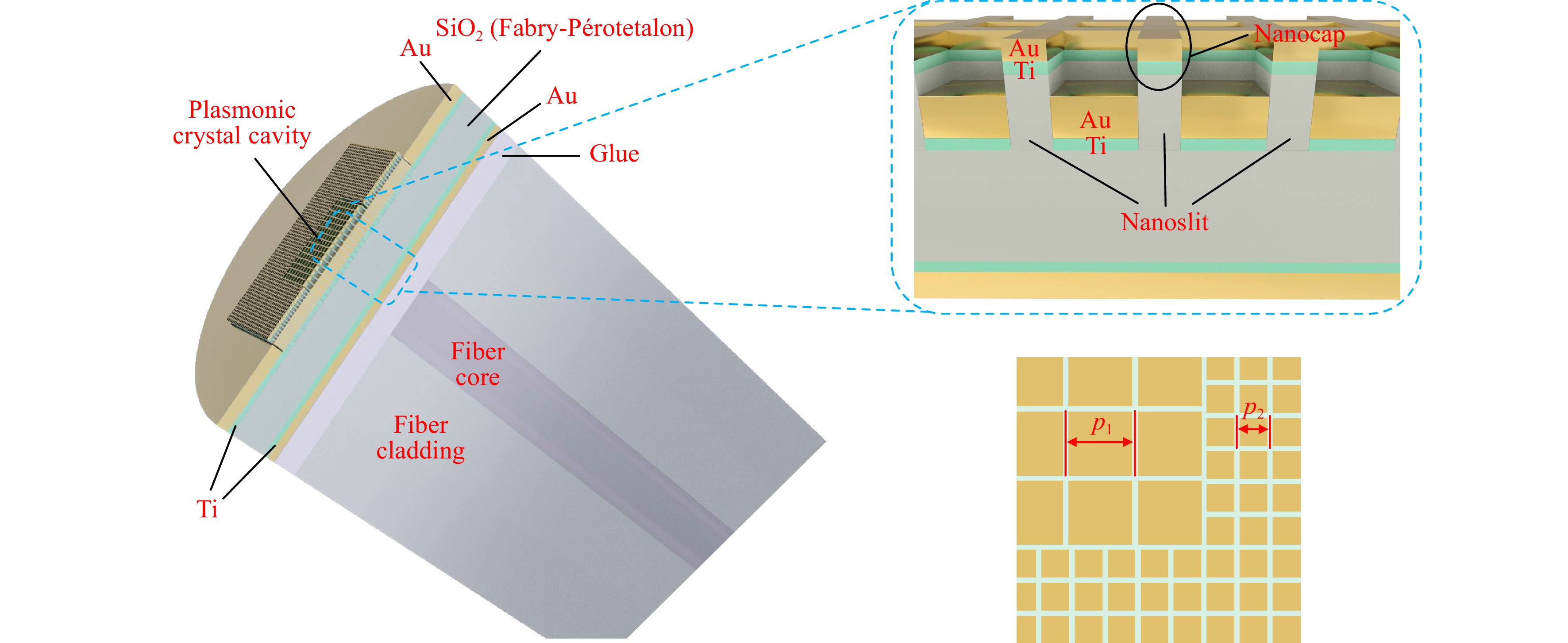
Fig. 1 Device Structure. Schematic illustration of a quasi-3D Fano resonance cavity on an SMF end-facet. Insets: top right, a zoom-in view of the nanocaps and nanoslits; bottom right, a zoom-in crossectional view along the center plane of the top gold film, showing a corner of the plasmonic crystal cavity.
-
As shown in Fig. 1, the device is composed of the SMF end-facet, a layer of ultraviolet (UV) epoxy glue, a bottom gold film of 20 nm thickness (the first reflection mirror of the etalon), a 230 nm thick SiO2 layer (the body of etalon), and the plasmonic crystal cavity in a 55 nm thick top gold film (the second reflection mirror of the etalon) in sequence. The plasmonic crystal consists of a square array of 50 nm wide nanoslits, which penetrate through the gold film and are filled with SiO2. There is a 5 nm thick gold nanocap above each slit. In addition, there are 2 nm titanium adhesion layers between the gold films and the SiO2 layer.
As illustrated in Fig. 1, the nanoslits divide the plasmonic crystal into a central region with a period p1, and a surrounding region with a period p2. For example, having p1=645 nm and p2=315 nm corresponds to an SPR resonance at 850 nm in a water environment. In Ref. 15, we conclude that, in the central region, the 2nd-order spatial Fourier component of the nanoslit array opens up a SPP bandgap near the center of the 1st Brillouin zone, and the 1st-order spatial Fourier component of the same nanoslit array couples the normally incident fiber-guided lightwave to the corresponding SPP bandedge. In the surrounding region, the 1st-order spatial Fourier component of the nanoslit array opens up a bandgap near the border of its 1st Brillouin zone, which forbids the fiber-coupled SPPs in the central region from escaping the cavity. As a result, SPPs are excited by the fiber guided lightwave and confined in the plasmonic crystal cavity. A detailed analysis of the nanoslit plasmonic crystal (without the nanocap), including its band diagram and modes, and another relevant cavity design using a defect state within the SPP bandgap can be found in Ref. 15,16.
Fig. 2a is a schematic illustration of a cross section of the plasmonic cavity coupled to a SMF (without the etalon) along the fiber axis. Note that the incident fiber-guided lightwave can be divided into two orthogonally polarized modes, each being polarized parallel to half of the slits, and being coupled to SPPs by the other half slits which are oriented in the orthogonal direction (which form a one-dimensional nanoslit grating). Therefore, we can approximately perform a two-dimensional (2D) simulation of the electromagnetic fields based upon this cross section profile. In the simulation, a broadband p-polarized lightwave in the SMF’s guided mode is incident upon the plasmonic cavity, and the reflected light is collected by the same SMF. The simulated device is immersed in water (refractive index 1.33); the fiber core has a refractive index of 1.45 and a diameter of 5 μm, the fiber cladding has a refractive index of 1.445 and a diameter of 125 μm; the central region of the plasmonic crystal is optimized to contain 16 periods, p1=645 nm, p2=315 nm, and the distance between the borders of the central and surrounding regions of the plasmonic crystal is optimized to 785 nm. The titanium adhesion layers are not included in the simulation here, whose effect will be discussed in the Device Fabrication section and Supplementary Information.
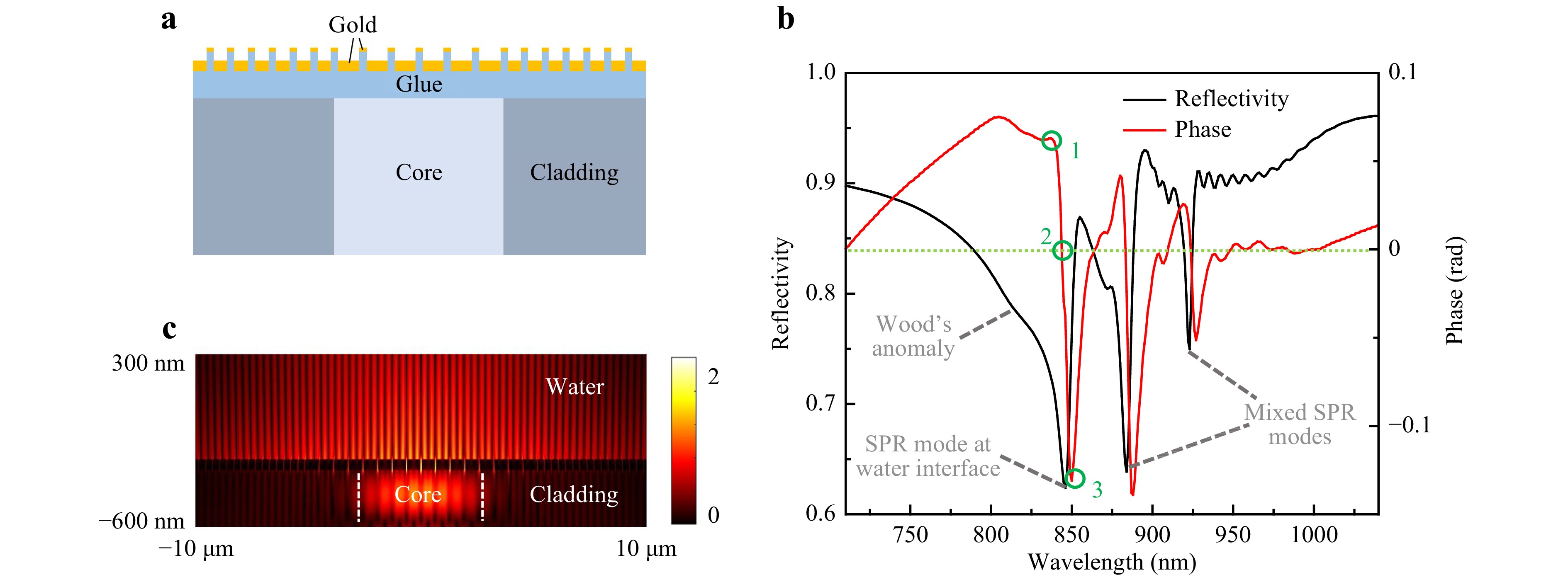
Fig. 2 Simulation of a bare plasmonic cavity. a Schematic illustration of the cross section of a plasmonic cavity coupled to a SMF, which was used for 2D FDTD simulation. b Simulated reflectivity and reflection phase spectra, p1 = 645 nm. The circled points correspond to maximum, zero and minimum phase shifts. c Electric field intensity distribution of the SPR mode at water interface, at the reflectivity dip’s apex.
The simulated reflection spectrum is shown in Fig. 2b, including both reflectivity and reflection phase. The spectrum shows Wood’s anomaly, an SPR mode at the gold film-water interface, and two mixed SPR modes which are distributed on both the gold film-water interface and the gold film-fiber interface15. The shortest wavelength SPR mode which is near 850 nm (a standard fiber-optic communication wavelength) will be used for sensing purpose. It has a Q value of 109. Its electric field intensity profile is shown in Fig. 2c. The SMF-coupled high Q values by using plasmonic crystal cavities were first reported by our group in 2016 and 201715,16. It had allowed using narrow-band fiber-coupled light-emitting diodes as photon sources, and it had improved the noise-equivalent LOD to 10−6 RIU by monitoring the centroid of the SPR dip in the reflectivity spectrum (wavelength interrogation). To date, such a LOD is still smaller than the best reported values of any other types of fiber end-facet SPR sensors by around two orders of magnitude. However, as shown in Fig. 2b, these devices were limited by their very low coupling efficiencies with SMF, resulting in a not more than 15% depth of the resonance dips in the fiber-guided reflectivity spectra. The low coupling efficiency significantly degraded the interrogated signal amplitudes and increased shot noises from the photon detection devices, e.g. a charge coupled device spectrometer.
In order to improve the SPR-SMF coupling efficiency, we resort to Fano resonance which is an effective method for coupling high-Q dark modes with external illumination and radiation29. As illustrated by Fig. 1, we built a F-P etalon that is comprised of the abovementioned plasmonic crystal cavity, a SiO2 layer and a bottom metallic layer. The plasmonic crystal cavity and the bottom metallic layer form the two reflection mirrors of the etalon, and the SiO2 layer accommodates the optical standing wave of the etalon. The design principle for the Fano resonance is to make the relatively low-Q etalon maximally coupled to the fiber-guided lightwave, then leverage the fast phase variation of the high-Q plasmonic crystal cavity to generate a narrow-linewidth resonance. Although the plasmonic crystal cavity is strongly under-coupled to light incident from its backside and only provides a tiny phase shift as shown in Fig. 2b, we will show the Fano effect is able to significantly enhance its resonance strength.
The thickness of the SiO2 layer was chosen to set the fundamental F-P mode at 850 nm, which is also close to our SPR wavelength. The thickness of the bottom metallic layer was chosen for a very low on-resonance reflectivity, or nearly critical coupling. By intentionally moving the SPR wavelength away from the F-P resonance, we simulated and plot the reflectivity of the etalon when coupled to an SMF, as shown in Fig. 3a. In the following, we will call it a non-SPR etalon. Then we let SPR move in and align with different regions of the non-SPR etalon reflectivity spectrum by tuning the nanoslit period, whose simulated reflectivities are shown in Fig. 3b−d. Comparing with Fig. 2b, the shallow SPR reflectivity dip is now converted to deep dips and high peaks with a much lower minimum reflectivity, and the reflectivity contrast within the SPR spectral range is significantly enhanced without sacrificing the Q value. In Fig. 3b−d, the corresponding bare plasmonic cavities’ maximum, zero and minimum reflection phase points are labeled with 1, 2 and 3. For example, the reflectivity points in Fig. 3c have the same wavelengths as the identically numbered phase points in Fig. 2b. Red, green and blue colors are used to designate the cavities with different periods which align differently with the etalon.
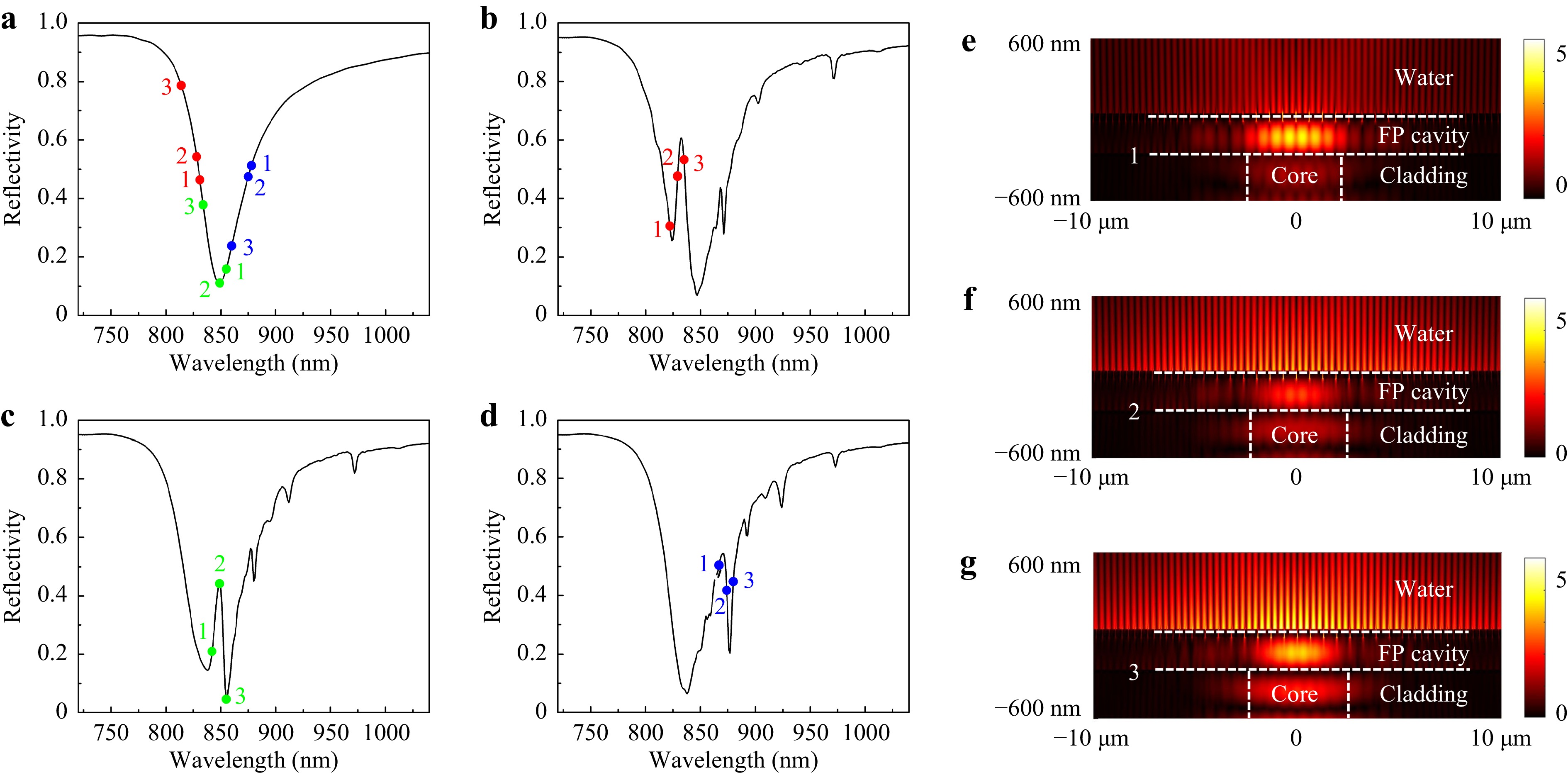
Fig. 3 Simulation of F-P etalon and Fano resonance. a Reflectivity spectrum of the non-SPR etalon. b−d Reflectivity spectra of Fano resonances, with the nanoslit period p1 = 620 nm (b), 645 nm (c) and 670 nm (d), respectively, and p2 proportionally scaled. e−g Electric field intensity distributions for points 1(e), 2(f) and 3(g) of the p1 = 620 nm Fano resonance.
The Fano resonance line-shapes can be qualitatively interpreted by an equivalent wavelength order reversal effect, as follows. If we take the plasmonic cavity’s reflectivity amplitude as a constant at different wavelengths (like in the case of strong over-coupling), both the non-SPR etalon and the SPR-coupled etalon’s reflectivity can be solely determined by its round-trip phase (except a small dispersion effect). This round-trip phase is a summation of the propagation phase in the SiO2 layer, the bottom metallic layer’s reflection phase and the plasmonic cavity’s reflection phase, the last of which is Δφ. Δφ shifts rapidly within the SPR spectral range, as shown in Fig. 2b. Therefore, we can obtain the SPR-coupled etalon’s reflectivity at any incident wavelength, λ, from the reflectivity of the non-SPR etalon at an equivalent wavelength, λ+Δλ. The wavelength shift, Δλ, provides a propagation phase change equal to Δφ to replace the plasmonic cavity, which can be obtained from Eq. 1,
$$ \left(\frac{{2\pi }}{\lambda } - \frac{{2\pi }}{{\lambda + \Delta \lambda }}\right)2n{{L - }}\Delta \phi = 0 $$ (1) where n and L are the refractive index and thickness of the SiO2 layer, respectively. As shown in Supplementary Fig. S1, when Δλ (or Δφ) is large enough, a sweeping of the incident wavelength will be turned into a sweeping of the equivalent wavelength that contains a reversed order (when the decrease of Δλ exceeds the increases of λ), which generates the Fano resonance line-shape.
The equivalent wavelength-shifted points on the non-SPR etalon reflectivity curve are labeled in Fig. 3a, using the same number and color combination to relate to the phase points of different cavities. For example, the red-1 point in Fig. 3a sits at the equivalent (shifted) wavelength which is obtained by substituting the red-labeled bare plasmonic cavity’s λ and Δφ at the maximum Δφ point (point 1) into Eq. 1. We can see that, the plasmonic cavities’ reflection phases reverse the wavelength order of points 1-2-3 in Fig. 3a, in which point 3 has the shortest equivalent wavelength and point 1 has the longest, in the opposite order to their original wavelengths. It is this reversal that generates the Fano resonance line-shapes in Fig. 3b−d.
While the above simple interpretation helps to design the Fano resonance structure, it doesn’t give accurate results due to the bare plasmonic cavity’s concomitant reflectivity change. Considering the plasmonic cavity’s reflectivity drop within the SPR spectral range, which makes the equivalent F-P resonance broader and shallower than the non-SPR etalon, the relation between most points in Fig. 3a and Fig. 3b−d approximately agrees with our simple model. However, for point green-2, it almost overlaps with the bare plasmonic cavity’s reflectivity dip’s apex and the non-SPR etalon’s (nearly) critical coupling wavelength. Therefore, its strong modification of the etalon’s mirror reflectivity breaks the critical coupling condition, and results in a sharp reflectivity peak. It is difficult to contain point green-3 in our simple model, which reaches a reflectivity even lower than the non-SPR etalon as in Fig. 3c, but is anticipated to have a much higher reflectivity as in Fig. 3a. This could be attributed to our model not including more complicated factors, e.g. higher order diffraction by the nanoslit grating into the etalon; near the critical coupling point, otherwise insignificant factors may become more important. Nevertheless, we note that the segment 1-2-3 in each of Fig. 3b−d approximately overlaps with the sharpest rise and fall of the reflectivity curve, which is attributed to the fast phase shift of the bare plasmonic cavities in this region.
The electric field intensity profiles for points red 1-3 are shown in Fig. 3e−g. Here, the points 1 and 3 correspond to relatively higher plasmonic cavity reflectivities (Fig. 2b), therefore they result in higher field intensities in the F-P cavity. At point 2, the higher coupling between plasmonic cavity and incident lightwaves (Fig. 2b) compensates for the weaker F-P field to generate a strong SPP field. The reflectivity drop at point 1 (Fig. 2b) is considerably attributed to Wood’s anomaly, so that its SPP coupling is relatively inefficient and its SPP field is the weakest of the three points.
Although the plasmonic cavity is only significantly under-coupled to the incident lightwave, as evidenced by the small phase shift range in Fig. 2b, the F-P resonance enhances the phase shift effect by multiple round-trip reflections and produces high contrast Fano resonances. In addition, the Fano resonance line-shape can be predesigned to be either a reflectivity dip or a reflectivity peak, by tuning the plasmonic cavity’s period or changing the refractive index of the solution.
For refractive index sensing applications, it is most common to monitor the centroid wavelength of the resonance spectra, in which the wavelength interrogation noise follows Eq. 2,
$$ {\lambda _{\rm c}} - \bar \lambda = \frac{{\displaystyle\sum\limits_i {({\lambda _i} - \bar \lambda ){I_i}} }}{{\displaystyle\sum\limits_i {{I_i}} }} $$ (2) where λc is the measured centroid wavelength (with noise),
$\bar \lambda $ is the precise centroid wavelength (without noise), i is the number for each pixel of the spectrometer, λi is the wavelength of pixel i, and Ii is the photon intensity or counts recorded by pixel i. The λc interrogation noise comes from the detection noise of I, the latter usually being shot noise. According to this equation, the noise of Ii at wavelengths away from$\bar \lambda $ contributes more to the noise of λc. Therefore, a high resonance peak with a low off-resonance background, as in the case of Fig. 3c, is the best choice for achieving a low noise-equivalent LOD. In the Sensing Experiment section, we will demonstrate an unprecedented low LOD for fiber end-facet SPR sensors by using this high-Q Fano resonance peak. -
Fig. 4 shows the flow chart of the device processing procedures. First, the Fano structure was fabricated on a quartz glass substrate. It began by depositing a 55 nm thick gold film on the substrate using electron beam evaporation. Then, a 120 nm thick polymethyl methacrylate (PMMA) e-beam resist layer was spin-coated, and the nanoslit pattern was written in the PMMA layer by electron beam lithography. Next, argon ion beam milling was used to transfer the nanoslit pattern into the gold film, with the PMMA layer as the milling mask. Here, the ion beam milling rate and time were controlled to etch beyond the gold film and into the glass substrate, by a depth of ~ 15 nm. Next, the PMMA was removed by oxygen plasma cleaning. A scanning electron microscopy (SEM) photograph of the nanoslit pattern at this stage is shown in Fig. 5a, showing the border between the central and surrounding regions. Afterwards, a 5 nm gold layer and a 2 nm titanium adhesion layer were deposited by electron beam evaporation in sequence, forming the caps covering the nanoslits. Next, the 230 nm SiO2 layer was deposited by plasma-enhanced chemical vapor deposition, at a temperature of 65 °C. Finally, another 2 nm titanium adhesion layer and a 20 nm gold layer were deposited by electron beam evaporation in sequence, to form the flat mirror of the etalon.
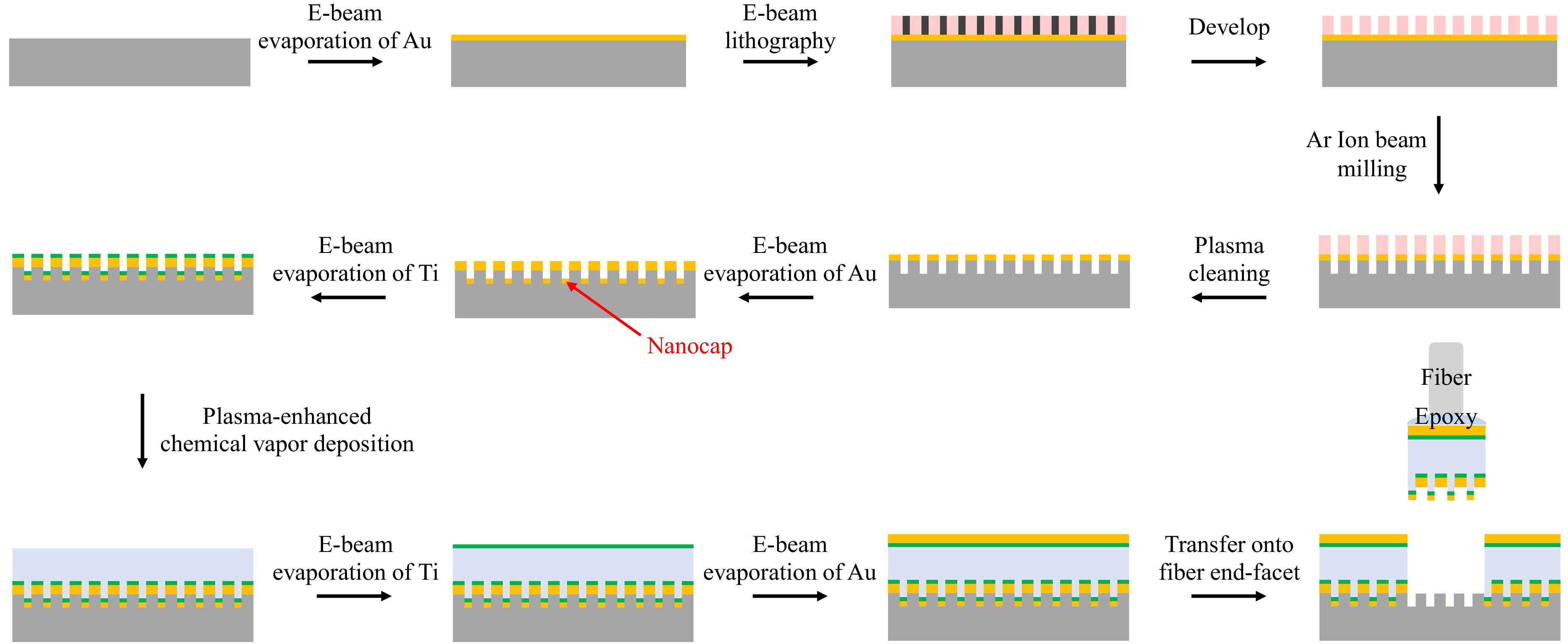
Fig. 4 Device fabrication procedures.
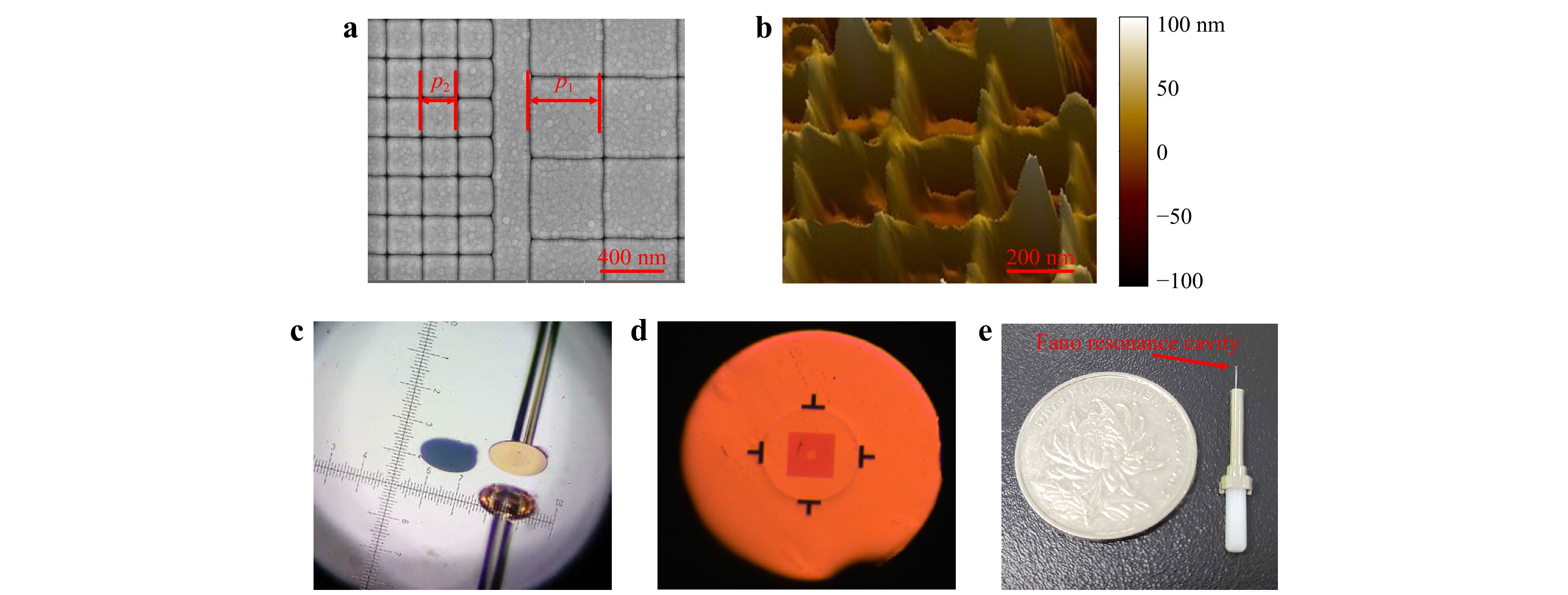
Fig. 5 Device fabrication results. a SEM photograph of the nanoslit pattern in the top gold film on a quartz substrate. b AFM photograph of the nanocap-slit structure, which had been transferred onto a fiber end-facet. c Stereomicroscope photograph of the transferring process. d Optical microscope photograph of the top view of a final device. e Device packaged in a fiber-optic connector; a coin is placed side by side to show the device’s size.
In the above process, the nanocap layer is crucial to form a low adhesion interface with the substrate. The low adhesion between noble metals and common dielectric and semiconductor substrates, which is mainly due to Van Der Waals force, has been widely employed to peel off and transfer a nanostructured noble metal film from its planar or templated substrate since its first report in 200930. This transferring technique has also become an efficient approach for mounting plasmonic sensing structures onto fiber end-facets15,24,25. However, in previous reports, the metal films contained perforations that penetrate through the entire thickness of the film in order to let the fiber-guided lightwave tunnel through, so as to excite SPPs on the metal film’s opposite side15,16 (for biosensing purposes, the SPPs must be on the solution side). These nanostructures are incompatible with further deposition of non-metallic materials, which would bind the nanostructures with the substrates firmly and disable the transferring. On the other hand, without the perforations, a continuous noble metal film would block the normally incident lightwave to the fiber side and disable efficient excitation of SPPs. Consequently, a new design that accommodates both the low adhesion and the SPP tunneling is required to make a 3D plasmonic nanostructure to be transferred. The nanocap design serves this purpose well, since the few nanometer SiO2 gap between the nanoslit and the metallic nanocap allows efficient SPP tunneling without impairing the transferring ability. In Supplementary Information, we show the recovery of SPP tunneling as the gap is opened, compared to a continuous gold film. Fig. 5b shows an atomic force microscopy (AFM) photograph of the top surface of a nanocap-slit structure, which had already been transferred onto the fiber end-facet. It contained a square array of protruding lines which are the nanocaps, confirming that the nanocaps had been peeled off and transferred.
In addition, the choice of material and thickness for the adhesion layers between the gold films and the SiO2 layer is important, in that the adhesion layers’ ohmic absorption strongly affects the F-P resonance. In Supplementary Information, we compare titanium and chromium layers with different thicknesses to illustrate this effect. A 2 nm titanium layer was chosen for the experiments for its lowest loss among the available choices. We also show in Supplementary Information that, according to simulation results, unevenness of the bottom metallic layer (between the SiO2 layer and fiber) caused by the nanoslits will not considerably affect the Fano resonance spectra when the unevenness is limited to a certain degree.
After completing device fabrication on the quartz glass substrate, we transferred the quasi-3D structures onto SMF end-facets as follows. The quartz glass substrate with the quasi-3D Fano resonance structure was fixed under a stereomicroscope. A UV epoxy glue was applied on the SMF end-facet, which was mounted on a multiple-axis motion stage. Then the fiber end approached the quartz glass substrate in a normal direction and contacted the Fano resonance cavity, while the alignment between the cavity and the fiber core was monitored through both microscope observation and measuring the fiber-guided reflectivity spectrum in real time. Once an optimum alignment was obtained, the glue was cured by a UV lamp. Finally, the fiber was pulled off, and the Fano resonance cavity was peeled off the quartz glass substrate and transferred to the SMF end-facet with a precise alignment. A photograph from the stereomicroscope is shown in Fig. 5c, in which the back sight of the fiber and its mirror image in the substrate are shown. A golden colored plate was on top of the fiber’s end-facet, which contained the transferred structure and whose size was determined by the applied glue; a nearby circularly shaped recess region (in blue color) on the substrate is where the plate was before being transferred.
A top view of one of the final devices is shown in Fig. 5d. The T-shaped dark areas are alignment marks to assist the transferring process. The circular rim enclosed by the alignment marks is the periphery of the 125 μm diameter fiber cladding. The square-shaped shaded area is the surrounding nanoslit array of the plasmonic cavity, which encloses a smaller square-shaped and less shaded area, which is the central nanoslit array. For convenience of sensing experiments, each fiber sensor was fixed in a standard fiber-optic connector, which included a metallic ferrule and a ceramic rod, as shown in Fig. 5e.
-
To confirm the Fano resonance spectra and obtain the noise-equivalent LOD, we have performed a physical adsorption experiment as follows. Note that a high optical signal-to-noise ratio (SNR), despite being the ultimate figure-of-merit to tell the optical performance of label-free sensors31, is only one of the prerequisites to achieve a real low LOD in biosensing applications (in terms of the target molecules’ concentration, molecular weight or affinity). In fact, a multiplicity of factors must be considered, and multi-disciplinary techniques should be taken, the overlooking of which has led to a number of dubious reports about extremely high sensitivities in the past32,33.
First, a device was dipped into solvents of different refractive indices, including methanol, water, acetone, ethanol and isopropanol. A super-luminescent diode photon source near 850 nm was coupled into a SMF, then the lightwave was routed to the device through a directional coupler, and the reflected lightwave was routed to a fiber-coupled spectrometer, as shown in Fig. 6a. The reflectivity spectra are plotted in Fig. 6b, showing the tuning of Fano resonance line-shape as the SPR resonance aligns to different regions of the etalon reflectivity spectrum. The experimental spectra agree well with the 2D simulation results. When SPR aligns to the side slopes of the etalon’s reflectivity spectrum, the depths of the resonance dips compare much favorably with the bare plasmonic crystal cavities15,16, reaching ~ 55%. When SPR overlaps with the center of the etalon’s reflectivity spectrum, a resonance peak of ~ 46% height with a low background was obtained.
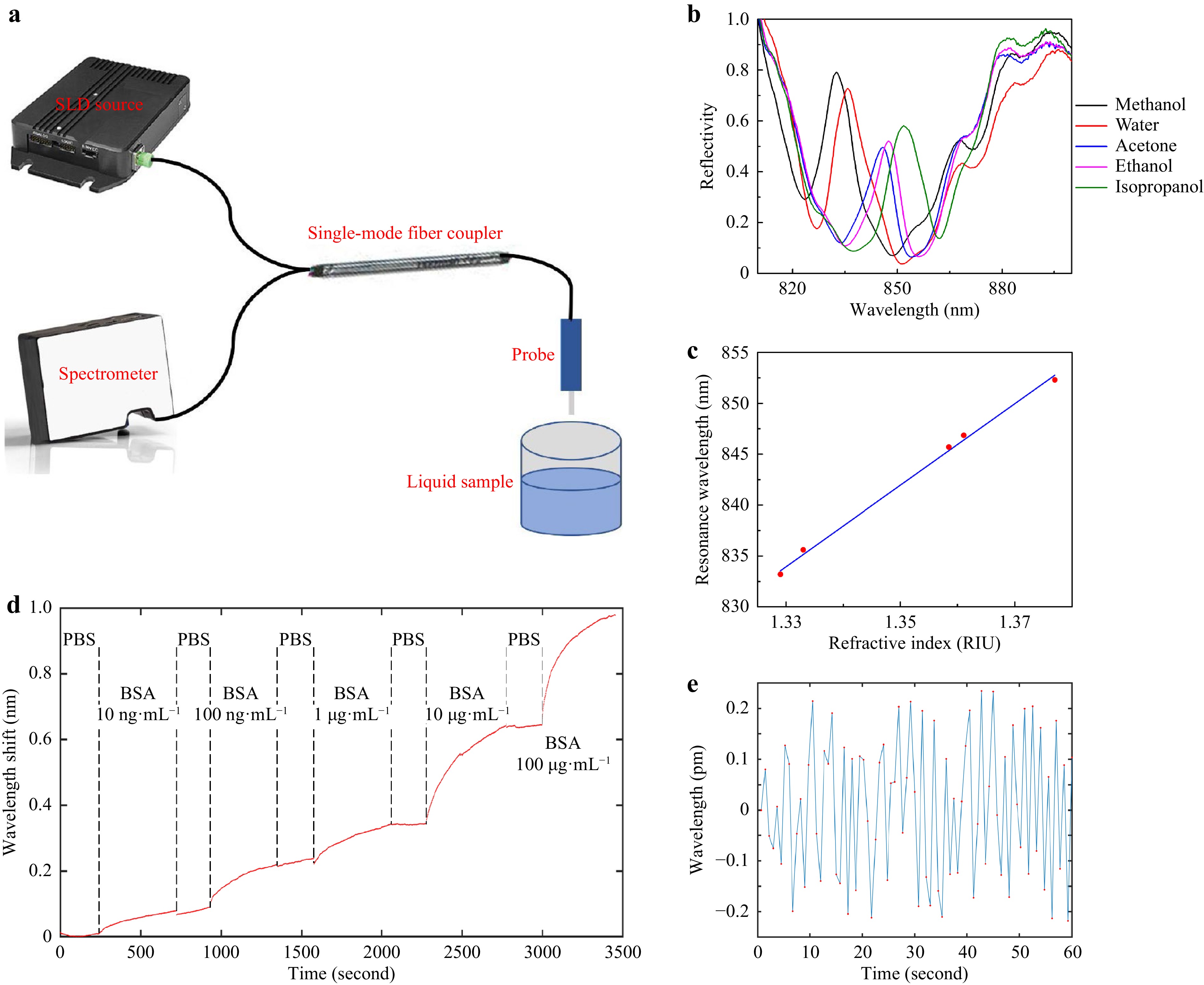
Fig. 6 Sensing Experiments. a Schematic of experiment setup. b Reflectivity spectra for different solvents. c Peak resonance wavelength versus refractive index for the solvents, with a linear fitting line. d Real-time monitoring of BSA adsorption at different concentrations. A couple of instantaneous signal jumps due to unidentified perturbations were removed from the plot. e Noise of baseline (sensor in PBS), data points labeled in red.
It is somewhat tricky to define the central wavelength of a Fano resonance, since it contains both a peak and a dip. For simplicity, we plot the peak wavelength versus refractive index in Fig. 6c. It shows a good linearity and a refractive index sensitivity of 411 nm RIU−1. However, as indicated by the 1-3 points in Fig. 3b−d, actually the shorter wavelength peak changes into the longer wavelength dip as the Fano resonance is tuned across the etalon’s reflectivity spectrum. In consideration of this effect, according to the peak wavelength of methanol reflectivity and the dip wavelength of isopropanol reflectivity, the SPR sensitivity is recalculated to be 625 nm RIU−1.
Second, we dipped the device in different concentrations of bovine serum albumin (BSA) in phosphate buffered saline (PBS) solution to read how the BSA molecules physically adsorb onto the gold surface in real time. The concentrations were increased from 10 ng mL−1 to 100 μg mL−1 in sequence, with a ten-time increase at each step, as shown in Fig. 6d. To assist the adsorption process, the samples were vibrated at 80 mm s−1 32. The sampling rate was around 0.75 second per point. The centroid wavelength was calculated using Eq. 2, where almost the complete Fano resonance peak was included in the calculation window. At the lowest concentration of 10 ng mL−1, SNR was over 100 (after subtracting baseline drift); but for 1 ng mL−1 measurement (not shown), the baseline fluctuation needs to be further reduced.
As indicated by Eq. 2, a high spectral peak with a low background is helpful to reduce the wavelength interrogation noise, since the high peak provides a large SNR for photon counting, while the low background minimizes the most important shot noise. Fig. 6e shows a zoom-in view of a part of a baseline, when the device was immersed in PBS. A root-mean-square wavelength interrogation noise of as low as 0.12 pm can be extracted from this plot, per one second integration time. This amounts to a noise-equivalent LOD of as low as 1.9 × 10⁻⁷ RIU. According to the reported LOD value for the bare plasmonic cavity in Ref. 15 and the spectrometer settings, and by using the theory in Ref. 31, the LOD of our Fano resonance cavity is estimated to be a bit lower than the measurement result. To find the reason for this discrepancy, we also included only the top half of the Fano resonance peak into Eq. 2 to recalculate the centroid wavelength, but the resulting wavelength noise wasn’t obviously increased as expected. It implicates that the experimental noise was quite possibly limited by some factors irrelevant to optical resonance, e.g. light path instability or electricity fluctuation.
-
In this work, quasi-3D Fano resonance cavities, in each of which a plasmonic crystal cavity is used as one of the mirrors of an F-P etalon, are mounted upon the end-facets of SMF’s. The Fano resonance line-shape can be flexibly tuned between reflectivity dip and peak by varying the geometric parameters of the cavity or the external refractive index. In the fiber-guided reflectivity spectra, resonances with heights or depths up to ~ 50% have been achieved experimentally, which breaks through the coupling efficiency bottleneck for high-Q fiber end-facet SPR biosensors (for sensors in water, refs. 15 and 16 reported experimental SPR spectral depths of 10-15%, here we reported SPR spectral height of ~55%). The refractive index LOD is improved by nearly an order of magnitude compared with bare plasmonic cavities, and is about three orders of magnitude lower than the best reported values for the other types of fiber end-facet SPR sensors (Refs. 15 and 16 reported noise-equivalent LOD of ~2 × 10⁻⁶ RIU, here we reported LOD of ~2 × 10⁻⁷ RIU). Such a LOD is essential for many sensing applications, e.g. measuring the interaction of small biomolecules20.
As to pursuing noise-equivalent LOD, using ultrahigh-Q or singularity micro-photonic devices coupled to tunable lasers, reports of LOD’s as low as 10−7~10−9 RIU were not uncommon4,34,35. However, it is important to point out that, when the noise-equivalent LOD has been reduced to the 10−7 RIU level, with state-of-the-art commercial technologies, the real LOD for biosensing will be limited by factors other than SNR, which include nonspecific binding, baseline drift, fluid mechanics, blank sample signal etc.20,32,33 (See Supplementary Information for more discussion). Here, we have demonstrated that it is indeed possible for fiber end-facet devices to overcome their inherent Q and coupling efficiency difficulties to become a new type of high-SNR label-free optical sensing devices. With a competent SNR, their inherent advantages will come together to make them standing out as a most efficient tool for rapid and point-of-care applications, which is why people have been working on miniature label-free sensors from the very beginning. These inherent advantages include a dip-and-read operation mode, minimal requirement on sample preparation and compact fiber-optic instruments32.
For fabricating 3D heterogeneous nanostructures at fiber end-facets, the noble metal nanocap-slit is such a unit that both allows SPP tunneling and ensures low adhesion with the substrates. Therefore, it is a useful and versatile interface for peeling off and transferring 3D SPR devices, which has been impossible before. We expect this 3D nanostructuring capability on fiber-tips to pave a pathway for the development of various new devices. In terms of manufacturing efficiency, while thousands of nanostructures can be fabricated simultaneously on the same planar wafer, the transferring process is also straightforward to be speeded and scaled up using modern automatic fiber-optic alignment technologies that have been recently commercialized by the semiconductor photonics industry.
The quasi-3D device design and quasi-3D heterogeneous nanofabrication capability developed here can also be implemented for other sensing applications. For example, the decrease of noise-equivalent LOD corresponds to the decrease of noise-equivalent pressure of these devices when they are used as hydrophones. In Ref. 11, we show that these devices have a broad bandwidth and a high stability for ultrasound detection, compared with traditional ultrahigh-Q optical resonators.
-
Simulation: The fiber-guided reflections and mode profiles of the devices were simulated by the finite-difference time-domain (FDTD) method using Lumerical FDTD Solutions. A 2D simulation window was used, with an anti-symmetric boundary condition along the axis of the fiber, and perfectly matched layer boundary conditions elsewhere. The photon source’s field profile was the fundamental mode of the fiber. A 50 μm wide monitor at 5 μm above the plasmonic cavity was used to monitor the reflected lightwave. The reflection phase was obtained by extrapolating and subtracting a smooth off-resonance phase. The grid size of the simulation mesh was 1~10 nm inside and near the cavity; we found that a 5 nm grid size was approximately good enough for simulating the nanocaps.
Spectrograph collecting and data processing: For each data point in Fig. 6d, e, the spectrometer recorded 500 spectrographs continuously, averaged them on board, and sent it to an external computer. The time interval between neighboring points was around 0.75 second. Next, the spectrograph was divided by the spectrum of the super-luminescent diode source, so that a normalized spectrograph was obtained, as shown in Fig. 6b. Following Eq. 2, the centroid wavelength of the Fano resonance peak in the normalized spectrograph was calculated and plotted in Fig. 6d, e. To obtain the root-mean-square noise for Fig. 6e, a polynomial fit was used to extract the signal’s slow fluctuation, which was used as the noiseless reference.
Sensor cleaning and storage: The sensors were cleaned by rinsing in 99.8% ethanol and deionized water before sensing experiments. After the experiments, they were dipped in a sucrose solution and air dried, so that the sensors were enclosed and protected by a dried sucrose droplet. The sucrose protection was dissolved by water at the beginning of the next experiment.
-
This work is supported by the National Natural Science Foundation of China (grant 61975253), the Science and Technology Commission of Shanghai Municipality (grant 21N31900200), the National Infrastructures for Translational Medicine (Shanghai), and the Lumieres (Xu Yuan) Biotechnology Company. Device fabrication is supported by the Center for Advanced Electronic Materials and Devices of Shanghai Jiao Tong University. Numerical simulation is supported by the Center for High Performance Computing of Shanghai Jiao Tong University.
A quasi-3D Fano resonance cavity on optical fiber end-facet for high signal-to-noise ratio dip-and-read surface plasmon sensing
-
Xiaqing Sun1, 2,
 ,
, - Zeyu Lei1,
- Hao Zhong1,
- Chenjia He1,
- Sihang Liu1, 3,
- Qingfeng Meng1,
- Qingwei Liu1,
- Shengfu Chen3,
- Xiangyang Kong2,
-
Tian Yang1, ,
- Light: Advanced Manufacturing 3, Article number: 46 (2022)
- Received: 21 July 2022
- Revised: 19 August 2022
- Accepted: 20 August 2022 Published online: 18 September 2022
doi: https://doi.org/10.37188/lam.2022.046
Abstract: Surface plasmon devices mounted at the end-facets of optical fibers are appealing candidates for rapid and point-of-care sensing applications, by offering a special dip-and-read operation mode. At present, these devices’ noise-equivalent limits-of-detection lag far behind the free-space counterparts, leaving them incapable of most biosensing applications. Here we report a quasi-3D Fano resonance cavity and its fabrication method to fundamentally improve the quality factor and coupling efficiency for fiber-coupled surface plasmon resonance. In this device, the Fano resonance combines the high coupling efficiency of a Fabry-Pérot etalon and the high quality factor resonance of a plasmonic crystal cavity. The quasi-3D device was fabricated on a planar substrate and transferred to a single-mode fiber end-facet, which requires a low-adhesion yet surface-plasmon-tunneling interface between the device and the planar substrate. Such an interface was realized with a nanocap-slit unit structure, of which the plasmonic crystal was consisted. A noise-equivalent limit of detection of ~ 10-7 RIU was experimentally obtained, allowing bovine serum albumin physical adsorption to be distinguished at ng mL-1 level concentrations. Therefore, breaking through the long-standing signal-to-noise ratio bottleneck, this work makes fiber end-facet surface plasmon devices into one of high sensitivity label-free sensing technologies. At the same time, it provides an enabling top-down fabrication technology for making 3D plasmonic structures on fiber end-facets at the nanometer scale.
Research Summary
Fiber-tip plasmonic sensing: Quasi-3D cavity design and fabrication
Fiber-tip plasmonic devices have great prospects for rapid and point-of-care label-free biosensing applications, due to the ultrasimple dip-and-read operation and the minimally invasive detection method. However, these devices’ signal-to-noise ratio (SNR) used to lag behind the free-space surface plasmon devices by several orders of magnitude. Tian Yang from China’s Shanghai Jiao Tong University and colleagues now report a quasi-3D plasmonic device on the end-facet of a single-mode optical fiber to overcome this challenge. In addition, they report a low-adhesion surface-plasmon-tunneling interface which lets the quasi-3D device be transferred from a planar substrate to the fiber tip. Having resolved the SNR bottleneck and the 3D nano-structuring difficulty, the authors anticipate fiber-tip plasmonic devices to become a really useful biosensing technology, for which they also discuss common pitfalls in evaluating physical devices for label-free biosensing.


Rights and permissions
Open Access This article is licensed under a Creative Commons Attribution 4.0 International License, which permits use, sharing, adaptation, distribution and reproduction in any medium or format, as long as you give appropriate credit to the original author(s) and the source, provide a link to the Creative Commons license, and indicate if changes were made. The images or other third party material in this article are included in the article′s Creative Commons license, unless indicated otherwise in a credit line to the material. If material is not included in the article′s Creative Commons license and your intended use is not permitted by statutory regulation or exceeds the permitted use, you will need to obtain permission directly from the copyright holder. To view a copy of this license, visit http://creativecommons.org/licenses/by/4.0/.

 DownLoad: