


-
To implement the display generation and optical combining functionality of AR, VR and MR HMDs, traditional optical elements and optical architectures have been developed throughout the past decades, especially for the defense market1 as the enterprise and consumer markets were just burgeoning. Early attempt at providing consumer grade smart glass display solution have had mixed results as in Google Glass V1, North Focus glasses, and other HMD systems from now defunct companies such as ODG, DAQRI, META, etc…
Traditional optics in HMDs include conventional refractive and reflective optics (circularly symmetric or freeform) as in Google Glass, ODG, META, but also conventional volume holographic optics as in North Focus, Intel Vaunt or Sony Smart Glasses. Although impressive optical performances have been demonstrated with such traditional optics and optical architectures for defense HMDs, the form factor, weight, size and wall plug efficiency of such systems were not at a level to provide adequate solutions for prosumer and consumer HMDs.
There are two main pillars2 defining the MR experience for the consumer market today: comfort and immersion. Comfort comes in various forms:
- wearable comfort –weight, size, center of gravity, thermal issues, …
- visual comfort –natural 3D cues over large FOV and high angular resolution
- vestibular comfort –stable and realistic world locked digital displays
- social comfort –socially acceptable form factor and operations
Immersion is defined as a multisensory perceptual experience3 (from audio to display, from gesture sensing to haptics). Immersion conveys to the user a high sense of realism4 which is a key feature to implement one of tomorrow’s key use cases for MR: the sense of presence5 of a virtual avatar interacting with the wearer of the HMD. Fig. 1 shows how immersion has increased dramatically when migrating from traditional flat screen displays to Near-To-Eye (NTE) displays.
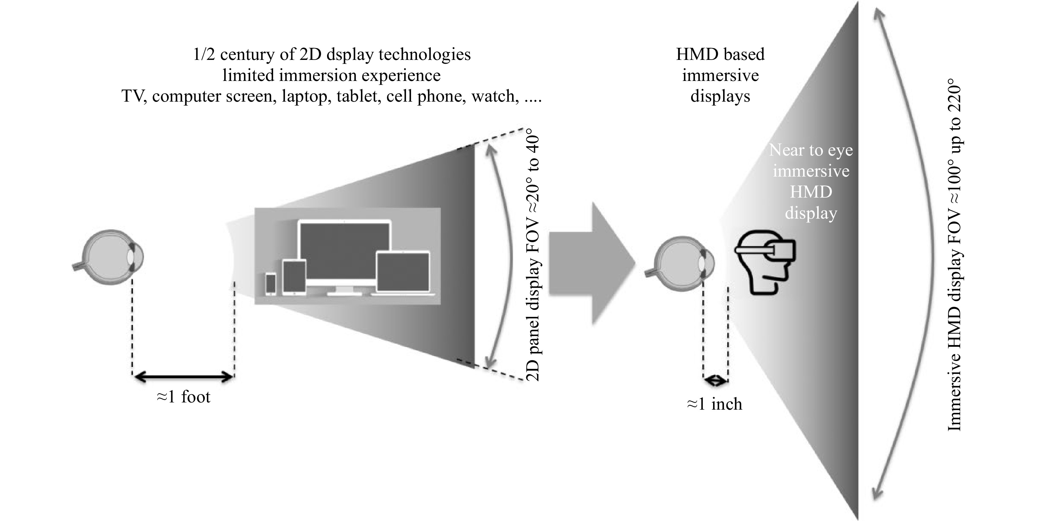
Fig. 1 Immersive NTE displays: a paradigm shift in personal information display.
In OST-HMS, the optical combiner is a key feature which acts as a transparent mirror or a transparent periscope shifting and expanding the entrance pupil generated by the display engine as depicted in Fig. 2.
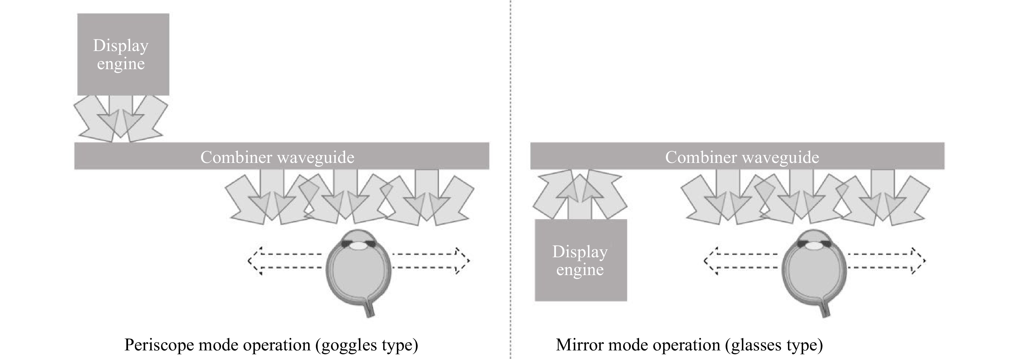
Fig. 2 The optical combiner: periscope mode or mirror mode with pupil shifting/expansion in transparent lightguide.
Periscope operation mode is best suited for goggle or helmet type HMDs where the display engine is located on the world side (temple or forehead) and mirror operation mode is best suited for smart glasses HMDs where the display engine is located in the glasses frames.
Both modes can provide a highly transparent operation and a generous eyebox by replicating the small pupil generated by the display engine. Key features of a waveguide combiner in either mode is optical efficiency, Modulation Transfer Function (MTF) decrease, transparency, ghosts and other parasitic optical artifacts that may be triggered with specific waveguide coupler technologies.
-
Considering the stringent form-factor, weight and size requirements to implement the display generation and optical combiner functionality, flat optics seems to be a de facto choice to implement the combiner task shown in Fig. 2.
However, simply considering flat optics might not be the best way to start the problem as flat optics do no necessarily mean flat optical systems, as described in Fig. 3
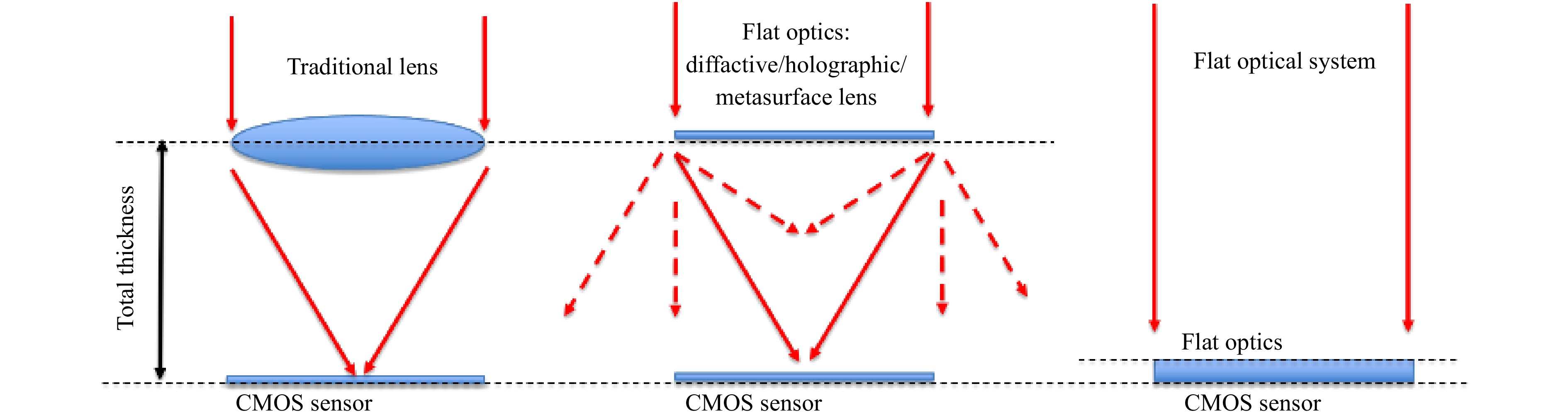
Fig. 3 Flat optics and flat optical systems.
Although flat optics can replace advantageously bulky refractive/reflective optics to reduce its overall weight, the size of the system might only be mildly improved. Flat optical system are our goal, and there are many ways to achieve this, by folding the space or redefining the imaging/display functionality.
Flat optics might seem also to be the cure to all refractive/reflective troubles when it comes to weight and size, and sometimes also to mass production via today’s optical lithographic or nanoimprint lithographic (NIL) systems. However, flat optical elements bare often much worse aberrations than their traditional curved optical elements counterparts as shown in Fig. 4.
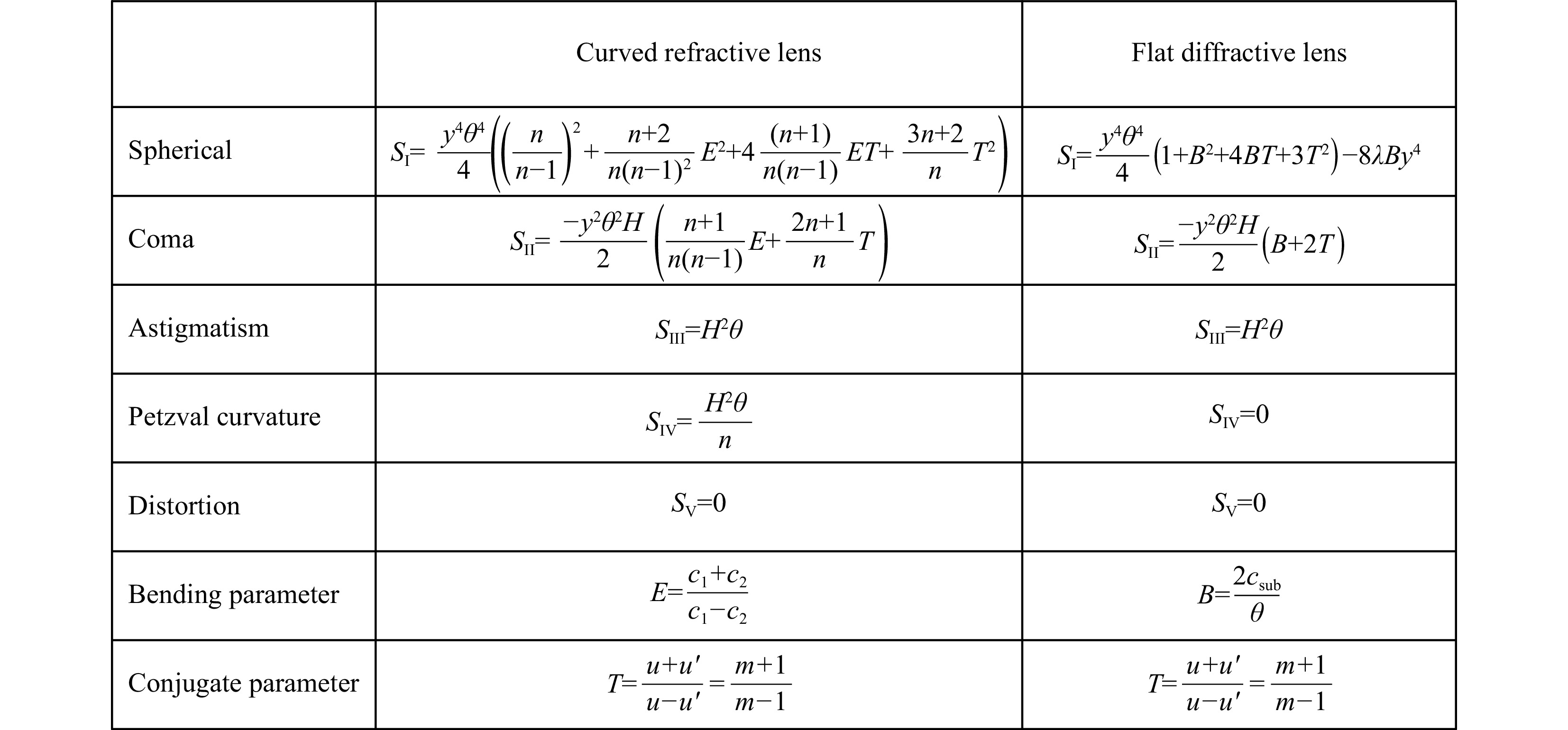
Fig. 4 Aberrations of curved refractive and flat diffractive lenses.
The other downsize of novel flat optics are their limited efficiency or throughput which, sometimes, reduces dramatically the wall plug efficiency of an HMD system, especially in OST mode. Below is a simple comparison of the maximum diffraction efficiency of a surface relief diffractive element when compared to its refractive counterpart (see Fig. 5), for many different lithographic fabrication techniques.
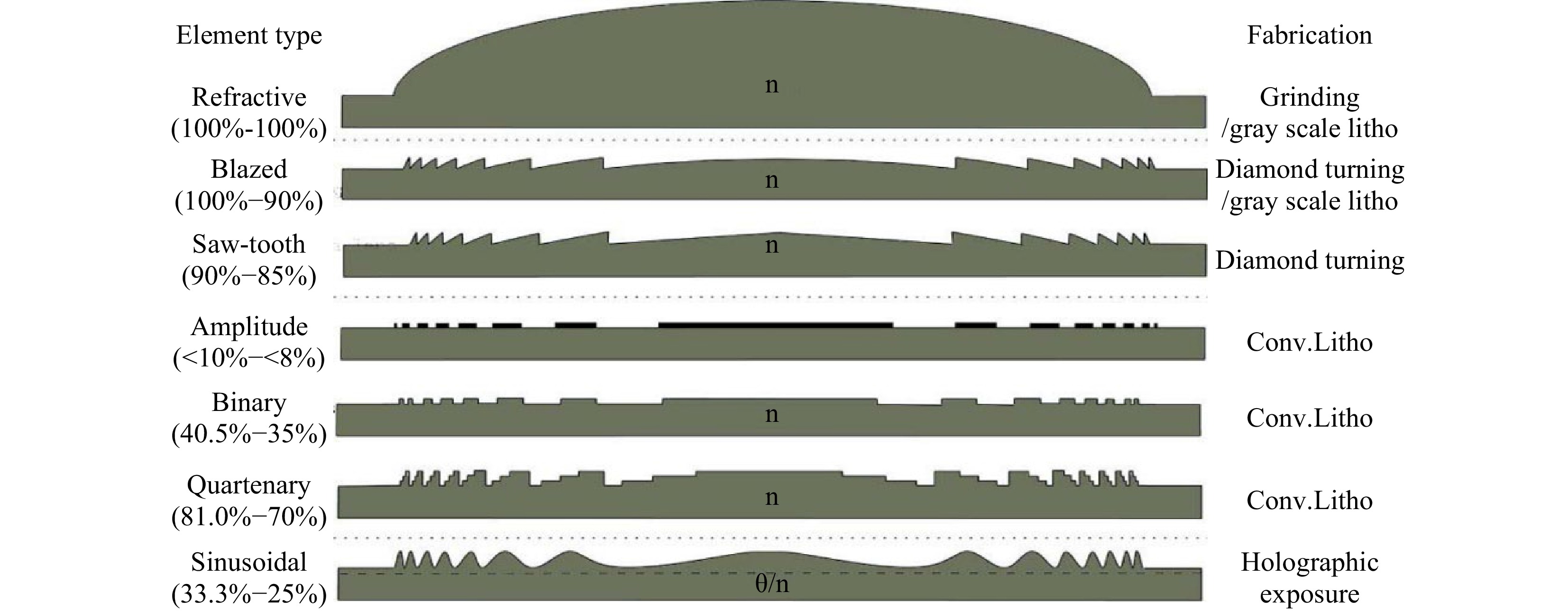
Fig. 5 Efficiency of curved refractive and flat surface relief diffractive lenses.
We review in the next two sections how flat optics have been implemented in both VR and AR HMDs to reduce the weight/size, improve the form factor, but also keep similar optical performances and efficiency, two key features of any wearable display.
-
Traditional direct view VR systems as they have been implemented since the early 70s, and still used today in many devices such as the latest Oculus Quest 2, comprise a magnifier lens and a display panel. However, that lens has been optimized in various ways to reduce its weight and size for ever increasing Field of Views (FOVs) as shown in Fig. 6. As one can see the weight and size is improved, and the lens gets flatter. However, the space between the display panel and the lens is unchanged, thus acting very little on the size of the overall system.
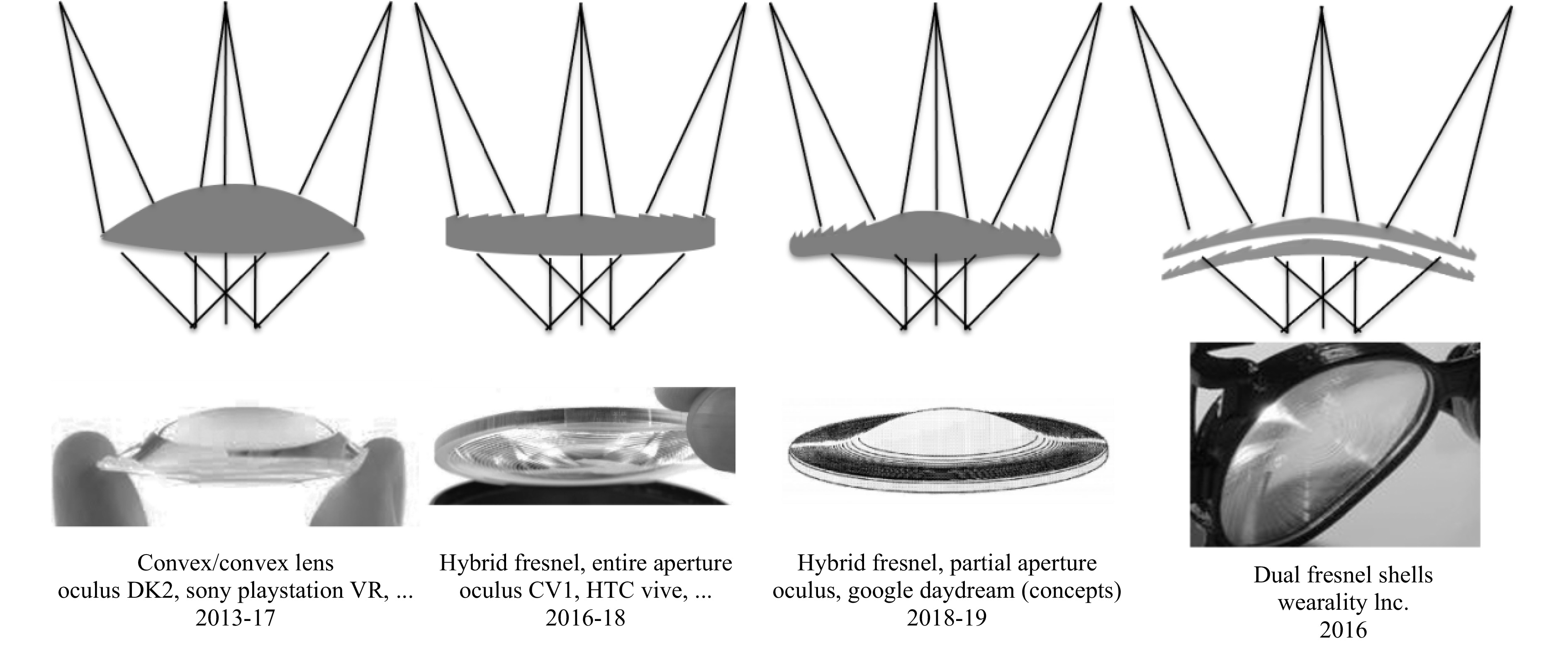
Fig. 6 Reducing the thickness of a VR lens.
In order to reduce the size of the overall system, the display architecture has to be altered by either increasing the Numerical Aperture (NA) of the system and reducing the size of the display or by introducing more lenses, either stacked or spatially multiplexed as described in Fig. 7.
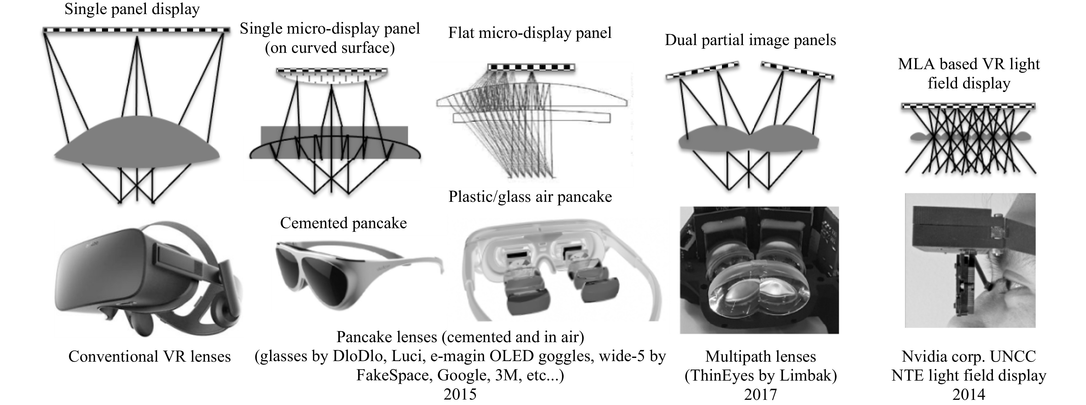
Fig. 7 Reducing the thickness of a VR display system.
Interestingly, Fig. 7 shows how a thicker lens (polarization pancake lens) can actually reduce the system thickness, which is totally counterintuitive and does not lean towards “thin optics” as a solution. However, thin optics as in compound lenses and Micro-Lens Arrays (MLAs) are indeed showing thinner optics providing thinner optical systems.
Other recent attempts have hybridized some of these concepts in very flat optical systems, by using micro-lenses and holographic polarization lenses with high NAs (see Fig. 8).
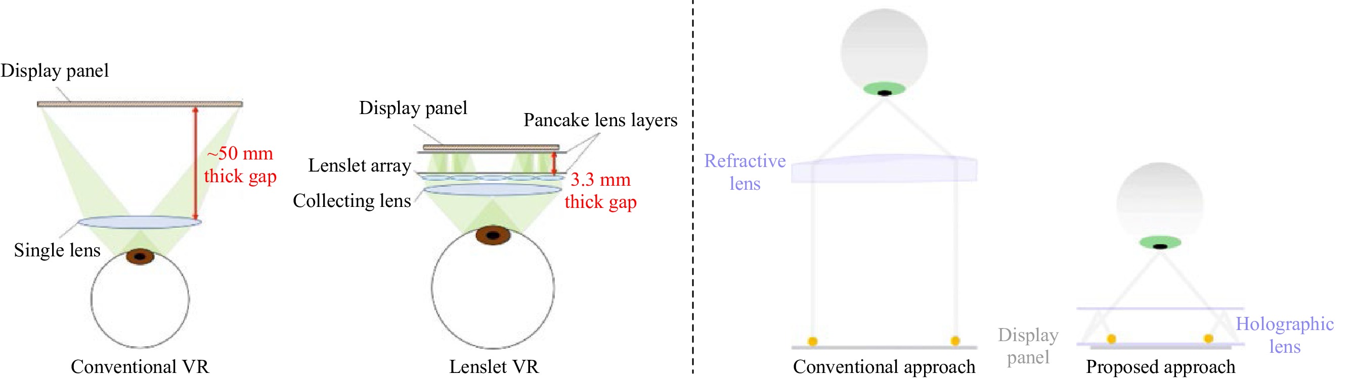
Fig. 8 Flat VR system using micro-lens arrays (left, Byoungho Lee, Seoul National University-2021), or holographic pancake optics (right, Andrew Maimone, Facebook reality Labs-2020)
Pancake lenses are folding the space with strong polarization optics (holograms) or layers (dichroics). However, a path further would be to fold the space independently from polarization, as it has been demonstrated by Prof Joseph Ford from UCSD with “origami lenses”. One of this architecture is depicted in Fig. 9.
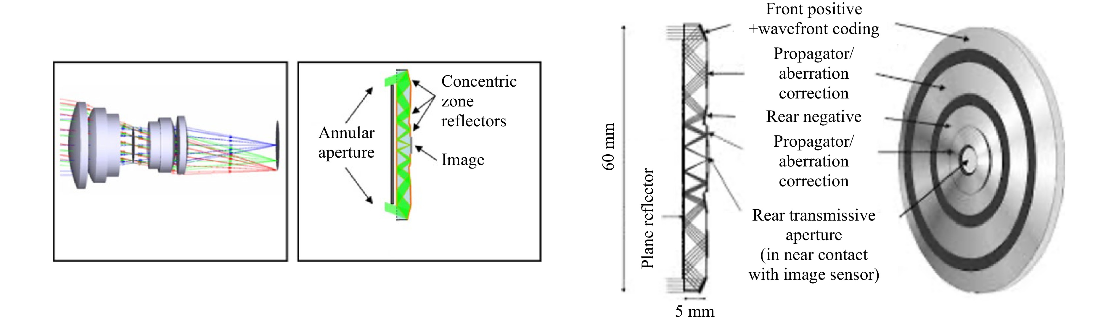
Fig. 9 Origami lenses (Prof. Joseph Ford, UCSD, 2008)
Although this is a space folding which reduces the aperture (all lens apertures are centered and toroidal), when going off-axis one can increase further the compactness of the system as it has been proposed very early on by Prof Juergen Jahns from Aachen University (1995). This space folding uses either metal reflective coatings or Total Internal Reflection (TIR) trapping via grating in-couplers as shown in Fig. 10.
Fig. 10 Planar optical systems (Prof. Juergen Jahns, 1995)
One other key feature of flat optics is that the efficiency can be modulated as per the number of surface reliefs in the fabrication process or the duty cycle of the fringes (in both surface relief and holographic), the depth of the surface relief elements, or the thickness of the holographic layer/emulsion. In traditional optical elements (such as in implementing the conventional Bokeh feature in photography), one may use an apodiser in conjunction with a refractive lens. If that lens is to be fabricated as a hologram or a surface relief diffractive (or even a metalens), the efficiency can thus be carefully modulated in order to produce a similar apodization effect but in a single element this time. Efficiency modulation provides a complex lens aperture function which in turn can then yield a specific point spread function, to enhance certain aspects of the image. Gaussian apodizations are used widely, but other more complex apodization can be used in order to combine high resolution and extended depth of focus (as depicted in Fig. 11).
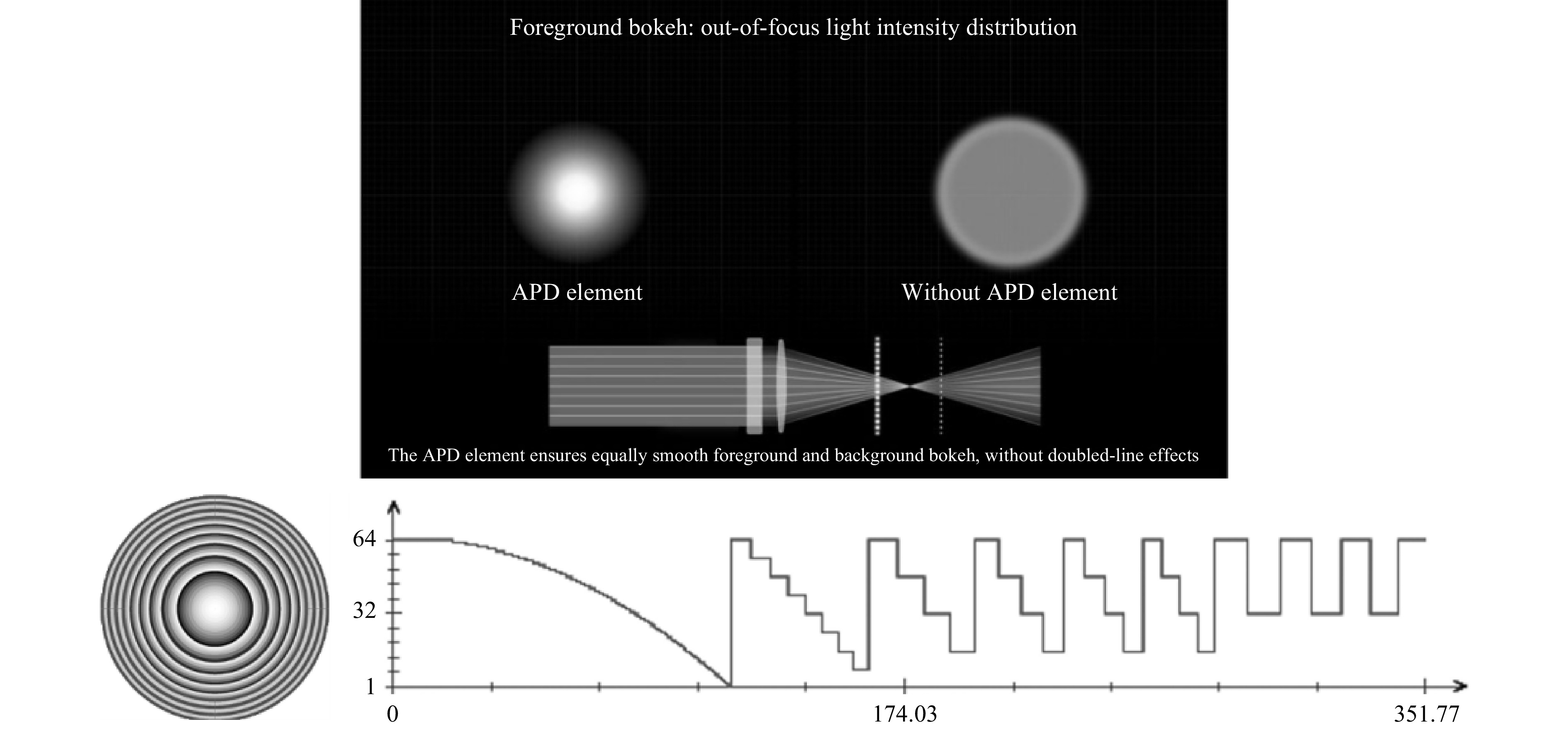
Fig. 11 Apodization of a diffractive lens by modulating the efficiency radially as a function of number of phase levels.
The drawback of that technique is that the undiffracted field might reduce the signal to noise ratio and increase scatter from an increased zero order or unwanted propagating orders.
Fig. 12 shows an example of a space multiplexed planar optical system implementing both structured illumination and extended depth of focus imaging functionality for 3D spatial scanning in a minimal form factor. We fabricated this element via a contact copy mask aligner with optical front/back alignment potential (Suss MA6-BA aligner) followed by ion beam etching of both surfaces.
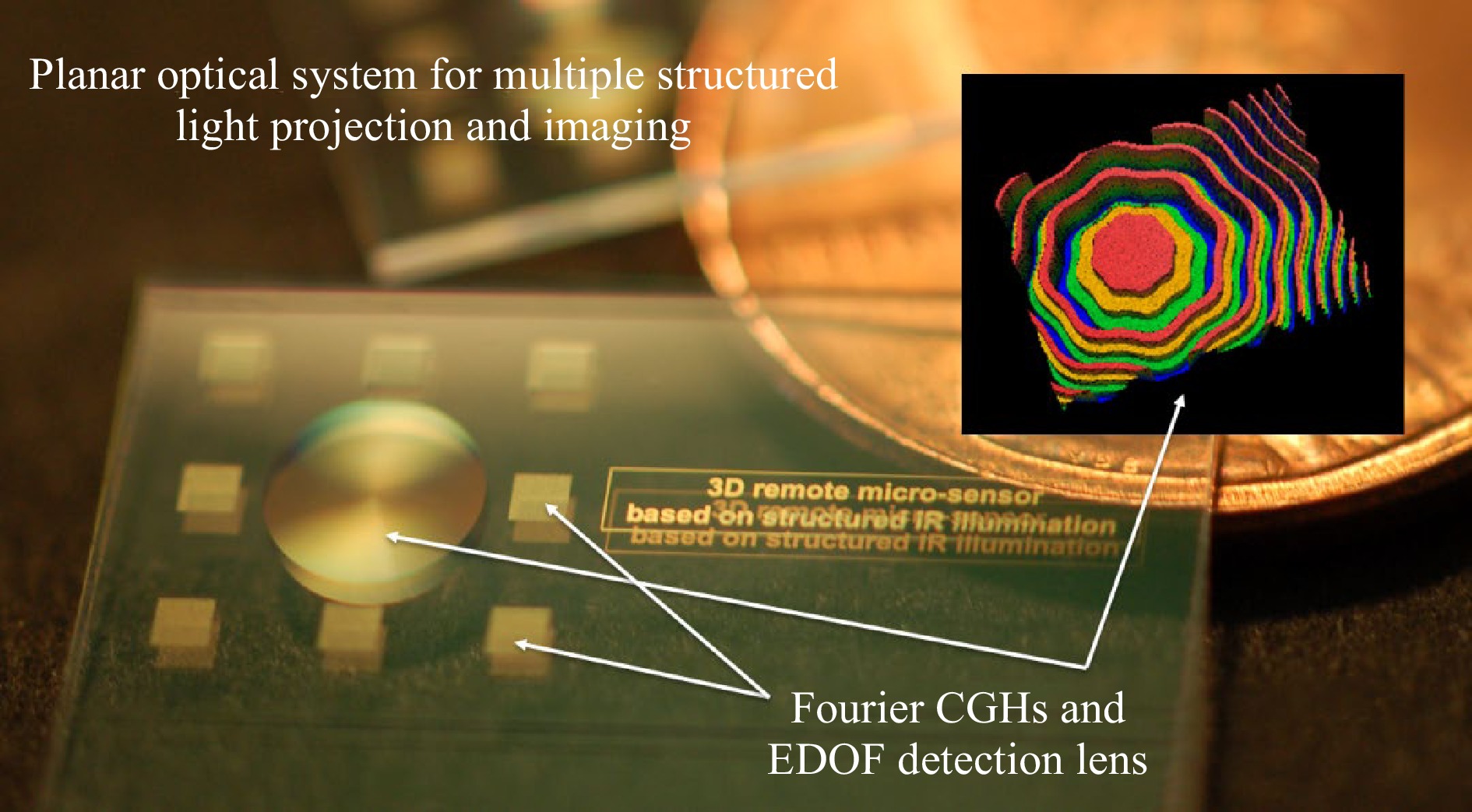
Fig. 12 Etched planar optical system including various CGHs and dual front-back extended depth of focus (EFOD) lens with anodization as a modulation of surface reliefs.
This planar optical system is aligned lithographically during its fabrication at sub-micron level and, thus, it is virtually impossible to misalign in the field since it is etched on the same fused silica substrate. Such accurate alignment and alignment resilience to environmental disturbances (temperature, shocks, vibrations) makes it perfect candidate for systems to be used in harsh environments.
In order to come up with the optimal waveguide combiner architecture for OST-HMDs, especially targeted to the consumer market, we will take advantage of such space folding architectures in planar waveguide systems. The next sections will be dedicated to such architectures.
-
The optical combiner is often the most complex and most costly optical element in the entire MR display architecture: it is the one component seen directly by the user and the one seen directly by the world. It often defines the size and aspect ratio of the entire headset. It is the critical optical element that reduces the quality of the see-through and the one that defines the eyebox size (and in many cases, also the FOV).
There are three main types of optical combiners used in most MR/AR/smart glasses today:
- Free-space optical combiners6,
- TIR prism optical combiners7 (and compensators), and
- Waveguide based optical combiners8-10.
When optimizing an HMD display system, the optical engine must be optimized in concert with the combiner engine11. Usually, a team that designs an optical engine without fully understanding the limitations and specifics of a combiner engine designed by another team, and vice versa, can result in a suboptimal system or even a failed optical architecture, no matter how well the individual optical building blocks might be designed.
Freeform TIR prism combiners are at the interface between free space and waveguide combiners. When the number of TIR bounces increases, one might refer to them as waveguide combiners. Waveguide combiner architectures are the topic of this review paper.
Waveguide combiners are based on TIR propagation of the entire field in an optical guide, essentially acting as a transparent periscope with a single entrance pupil and often many exit pupils12.
The primary functional components of a waveguide combiner consists of the input and output couplers. These can be either simple prisms, micro-prism arrays, embedded mirror arrays, surface relief gratings, thin or thick analog holographic gratings, metasurfaces, or resonant waveguide gratings. All of these have their specific advantages and limitations, which will be discussed here. Waveguide combiners have been used historically or tasks very different from AR combiner, such as planar optical interconnections13 and LCD backlights14,15.
Waveguide combiners are an old concept, some of the earliest IP dates back to 1976 and applied to HUDs. Fig. 13a shows a patent by Juris Upatnieks dating back 1987, a Latvian/American scientist and one of the pioneers of modern holography16, implemented in a di-chromated gelatin (DCG) holographic media. A few years later, one-dimensional eyebox expansion (1D EPE) architectures were proposed as well as a variety of alternatives for in- and out- couplers technologies, such as surface relief grating couplers by Thomson CSF (Fig. 13b). Fig. 13c shows the original 1991 patent for a waveguide-embedded partial mirror combiner and exit pupil replication (All of these original waveguide combiner patents have been in the public domain for nearly a decade17-19).
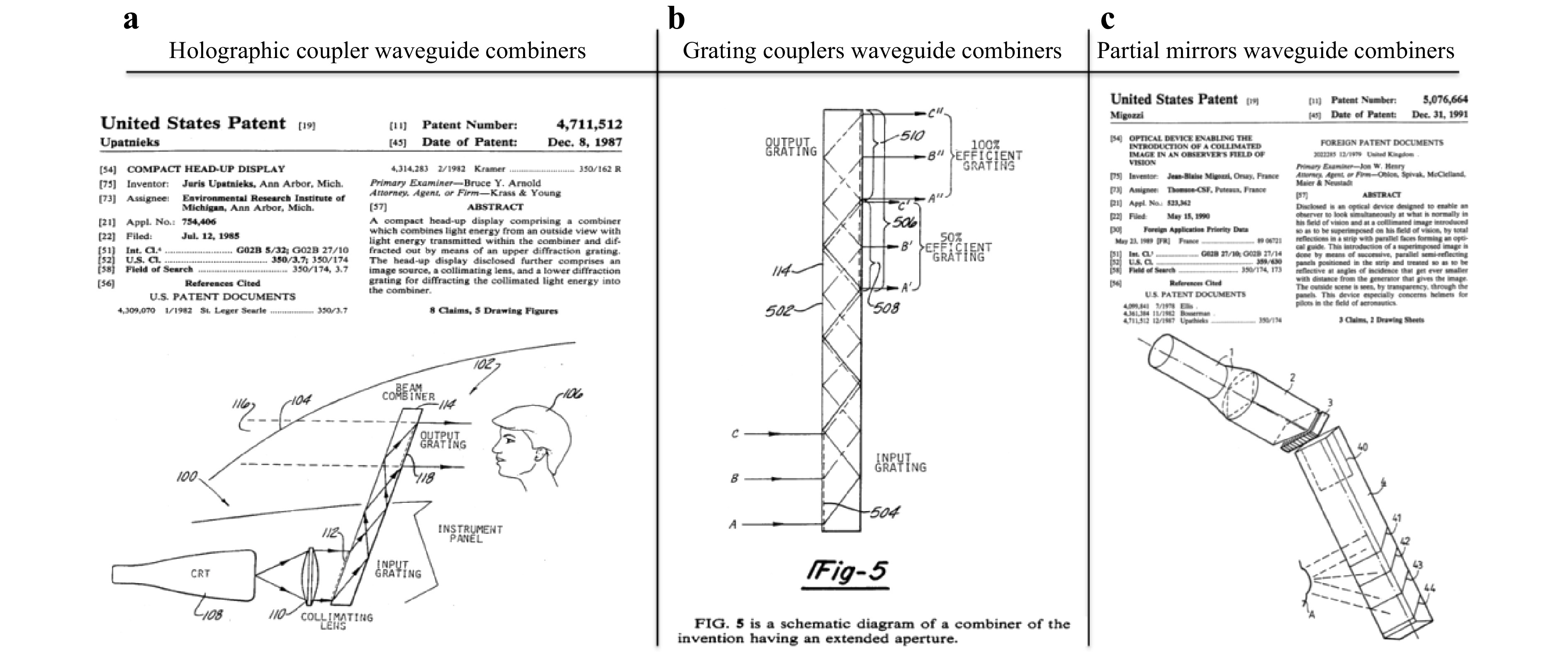
Fig. 13 a Original waveguide combiner patents including holographic (1987), b surface relief grating (1989), and c partial mirrors (1991) for HUD and HMD applications.
-
One can take the concept of a flat waveguide with a single curved extractor mirror (Epson Moverio BT300) or freeform prism combiner, or a curved waveguide with curved mirror extractor, to the next level by multiplying the mirrors to increase the eyebox (see the Lumus LOE waveguide combiner) or fracturing metal mirrors into individual pieces (see the Optinvent ORA waveguide combiner or the LetinAR waveguide combiner using fractured mirrors instead of cascaded partial mirrors20-23).
While fracturing the same mirror into individual pieces can increase see-through and depth of focus, the use of more mirrors to replicate the pupil is a bit more complicated, especially in a curved waveguide where the two exit pupils need to be spatially de-multiplexed to provide a specific mirror curvature to each pupil to correct for image position: this limits the FOV in one direction so that such overlap does not happen.
Fig. 14 summarizes some of the possible design configurations with such waveguide mirror architectures. Note that the grating- or holographic-based waveguide combiners are not listed here; they are the subject of the next sections.
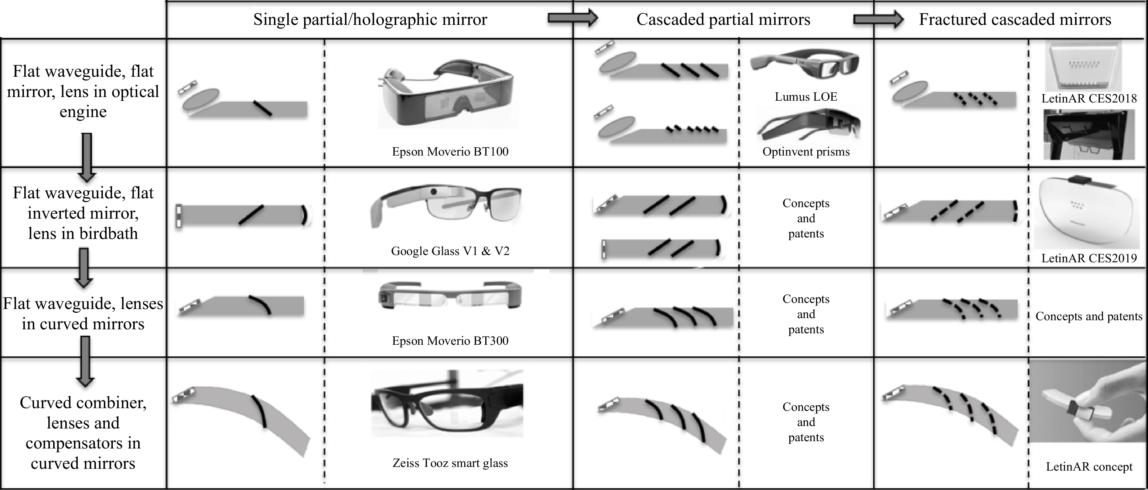
Fig. 14 From single to multiple mirrors in reflective waveguides.
Fig. 14 shows that many of the waveguide combiner architectures mentioned in this section can be listed in this table24,25. Mirrors can be half-tone (Google Glass, Epson Moverio), dielectric (Lumus LOE), have volume holographic reflectors (Luminit or Konica Minolta), or the lens can be fractured into a Fresnel element (Zeiss Tooz Smart Glass). In the Optinvent case, we have a hybrid between fractured metal mirrors and cascaded half-tone mirrors. In one implementation, each micro-prism on the waveguide has one side fully reflective and the other side transparent to allow see-through.
In the LetinAR case, all fractured mirrors are reflective, can be flat or curved, and can be inverted to work with a birdbath reflective lens embedded in the guide.
Even though the waveguide might be flat, when using multiple lensed mirrors, the various lens powers will be different since the display is positioned at different distances from these lensed extractors. When the waveguide is curved, everything becomes more complex, and the extractor mirror lenses need to compensate for the power imprinted on the TIR field at each TIR bounce in the guide. In the case of curved mirrors (either in flat or curved waveguides), the exit pupils over the entire field cannot overlap since the power to be imprinted on each exit pupil (each field position) is different (Moverio BT300 and Zeiss Tooz Smart Glass). This is not the case when the extractors are flat and the field is collimated in the guide (Lumus LOE).
-
Two-dimensional eyebox expansion is desired (or required) when the input pupil cannot be generated by the optical engine over an aspect ratio tall enough to form the 2D eyebox, due to the FOV (etendue limitations) and related size/weight considerations. A 2D exit pupil expansion (2D EPE) is therefore required (see Fig. 15). 2D expansion can now be performed with either diffractive, holographic or even reflective couplers as in the Lumus Maximus waveguide (2020).
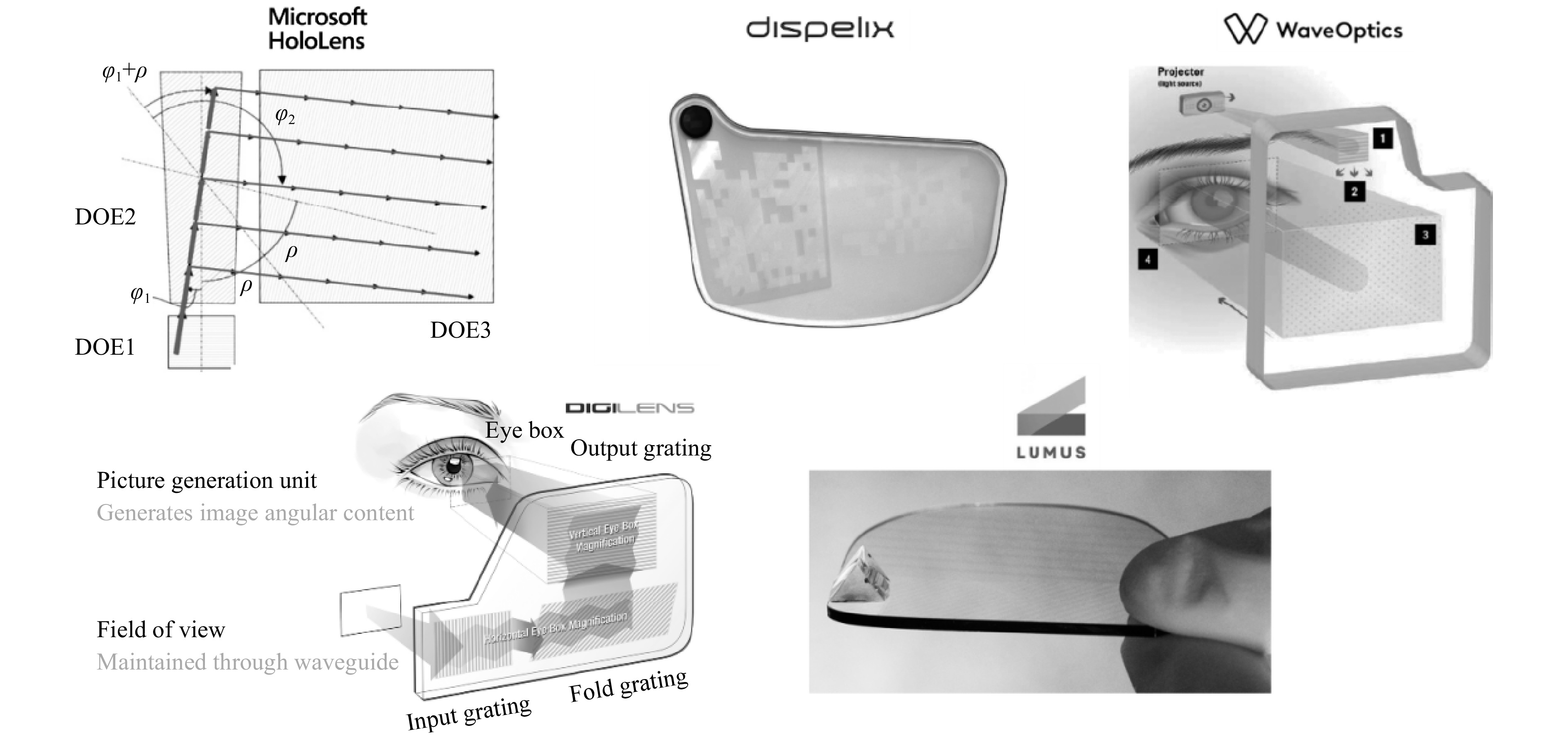
Fig. 15 2D pupil replication architectures in planar optical waveguide combiners.
While holographic recording or holographic volume gratings are usually limited to linear gratings, or gratings with slow power (such as off-axis diffractive lenses), surface relief gratings can be either 1D or 2D, linear or quasi arbitrary in shape. Such structures or structure groups can be optimized by iterative algorithms (topological optimization) rather than designed analytically.
Holographic recording, sometimes also called interference lithography when used to create patterns in a resin to be etched in a substrate (such as a nanoimprint master for waveguides) are not limited to linear fringes, but can also produce much more complex structures, such as 2D gratings or even computer generated holograms (CGH) when a digital CGH is used as a reference beam.
-
The coupler element is the key feature of a waveguide combiner. The TIR angle is dictated by the refractive index of the waveguide, not the refractive index of the coupler nanostructures. Very often, the index of the coupler structure (grating or hologram) prescribes the angular and spectral bandwidth over which this coupler can act, thus impacting the color uniformity over the FOV and eyebox.
Numerous coupler technologies have been used in industry and academia to implement the in-coupler and out-couplers, and they can be defined either as refractive/reflective or diffractive/holographic coupler elements.
-
A prism is the simplest TIR in-coupler, and can be very efficient. A prism can be bounded on top of the waveguide, or the waveguide itself can be cut at an angle, to allow normal incident light to enter the waveguide and be guided by TIR (depending on the incoming pupil size). Another way uses a reflective prism on the bottom of the waveguide (metal coated). Using a macroscopic prism as an out-coupler is not impossible, and it requires a compensating prism for see-through, with either a reflective coating or a low-index glue line, as done in the Oorym (Israel) lightguide combiner concept.
-
Cascaded embedded mirrors with partially reflective coatings are used as out-couplers in the Lumus (Israel) Lightguide Optical Element (LOE) waveguide combiner. The input coupler remains a prism. As the LOE is composed of reflective surfaces, it yields good color uniformity over the entire FOV. As with other coupler technologies, intrinsic constraints in the cascaded mirror design of the LOE might limit the FOV26. See-through is very important in AR systems: the Louver effects produced by the cascaded mirrors in earlier versions of LOEs have been reduced recently thanks to better cutting/polishing, coating, and design. Two dimensional pupil expansion in LOEs have been recently succcesfully demonstrated by Lumus in their latest Maximus X-Lens and Z-lens waveguide designs. High MTF, great color uniformity and high efficiency are key attributes of all reflective waveguide combiners.
-
Micro-prism arrays are used in the Optinvent (France) waveguide as out-couplers20. The in-coupler here is again a prism. Such microprism arrays can be surface relief or index matched to produce an unaltered see-through experience. The micro-prisms can all be coated uniformly with a half-tone mirror layer or can have an alternance of totally reflective and transmissive prism facets, provide a resulting 50% transmission see-through experience. The Optinvent waveguide is the only flat waveguide available today as a plastic guide, thus allowing for a consumer-level cost for the optics. The micro-prism arrays are injection molded in plastic and bounded on top of the guide. Focus lens can also be integrated in a flat waveguide by adding a slight curvature to the extraction prisms. This is possible as such elements are pressure molded in a mold using free-form diamond turned metal inserts rather than cut in glass as embedded cascaded mirrors.
-
Transparent volume holograms working in reflection mode—as in di-chromated gelatin (DCG), bleached silver halides (Slavic or Ultimate Holography by Yves Gentet), or more recently photopolymers such as Bayfol® photopolymer by Covestro/Bayer, (Germany)27, and photopolymers by DuPont (US), Polygrama (Brazil), or Dai Nippon (Japan)—have been used to implement in- and out-couplers in waveguide combiners. Such photopolymers can be sensitized to work over a specific wavelength or over the entire visible spectrum (panchromatic holograms).
Photopolymer holograms do not need to be developed as DCG, nor do they need to be bleached like silver halides. A full-color hologram based on three phase-multiplexed single-color holograms allows for a single plate waveguide architecture, which can simplify the combiner and reduce weight, size, and costs while increasing yield (no plate alignment required). However, the efficiency of such full-RGB phase-multiplexed holograms are still quite low when compared to single-color photopolymer holograms.
Also, the limited index swing of photopolymer holograms allows them to work more efficiently in reflection mode than in transmission mode (allowing for better confinement of both the wavelength and angular spectrum bandwidths).
Examples of photopolymer couplers include Sony LMX-001 Waveguides for smart glasses and the TrueLife Optics (UK) process of mastering the hologram in silver halide and replicating it in photopolymer.
Replication of the holographic function in photopolymer through a fixed master has proven to be possible in a roll-to-roll operation by Bayer/Covestro (Germany). Typical photopolymer holographic media thicknesses range from 16–70 microns, depending on the required angular and spectral bandwidths.
Covestro photopolymer replication technologies such as roll to plate or roll to roll can be used for volume production of such holographic optics, and used in coupler applications, both for AR, but also for larger areas such as in automotive/avionics HUDs and smart windows.
-
When the index swing of the volume hologram can be increased, the efficiency gets higher, and the operation in transmission mode becomes possible. This is the case with Digilens’ proprietary holographic polymer dispersed liquid crystal (H-PDLC) hologram material28. Transmission mode requires the hologram to be sandwiched between two plates rather than laminating a layer on top or bottom of the waveguide as with photopolymers, DCG, or silver halides. Digilens’ H-PDLC has the largest index swing today and can therefore produce strong coupling efficiency over a thin layer (typically four microns or less). H-PDLC material can be engineered and recorded to work over a wide range of wavelengths to allow full-color operation.
-
Increasing the index swing can optimize the efficiency and/or angular and spectral bandwidths of the hologram. However, this is difficult to achieve with most available materials and might also produce parasitic effects such as haze. Increasing the thickness of the hologram is another option, especially when sharp angular or spectral bandwidths are desired, such as in telecom spectral and angular filters. This is not the case for an AR combiner, where both spectral and bandwidths need to be wide (to process a wide FOV over a wide spectral band such as LEDs). However, a thicker hologram layer also allows for phase multiplexing over many different holograms, one on top of another, allowing for multiple Bragg conditions to operate in concert to build a wide synthetic spectral and/or angular bandwidth, as modeled by the Kogelnik theory29. This is the technique used by Akonia, Inc. (a US start-up in Colorado, formerly InPhase Inc., which was originally funded and focused to produce high-density holographic page data-storage media, ruled by the same basic holographic phase-multiplexing principles30).
Thick holographic layers, as thick as 500 microns, work well in transmission and/or reflection modes, but they need to be sandwiched between two glass plates. In some specific operation modes, the light can be guided inside the thick hologram medium, where it is not limited by the TIR angle dictated by the index of the glass plates. As the various hologram bandwidths build the final FOV, one needs to be cautious in developing such phase-multiplexed holograms when using narrow illumination sources such as lasers.
Replication of such thick volume holograms are difficult in roll-to-roll operation, as done with thinner single holograms (Covestro Photopolymers, H-PDLC), and require multiple successive exposures to build the hundreds of phase-multiplexed holograms that compose the final holographic structure. However, this can be relatively easy with highly automated recording set-ups as the ones developed by the now-defunct holographic page data-storage industry (In-Phase Corp., General Electric, etc.).
Note that although the individual holograms acting in slivers of angular and spectral bandwidth spread the incoming spectrum like any other hologram (especially when using LED illumination), the spectral spread over the limited spectral range of the hologram is not wide enough to alter the MTF of the immersive image and thus does not need to be compensated by a symmetric in- and out-coupler as with all other grating or holographic structures31. This feature allows this waveguide architecture to be asymmetric, such as having a strong in-coupler as a simple prism: a strong in-coupler is always a challenge for any grating or holographic waveguide combiner architecture, and a macroscopic prism is the best coupler imaginable.
Fig. 16 shows both thin and thick volume holograms operating in reflection and/or transmission modes. The top part of the figure shows a typical 1D EPE expander with a single transmission volume hologram sandwiched between two plates. When the field traverses the hologram downwards, it is in off/Bragg condition, and when it traverses the volume hologram upwards after a TIR reflection, it is in an on/Bragg condition (or close to it), thereby creating a weak (or strong) diffracted beam that breaks the TIR condition.
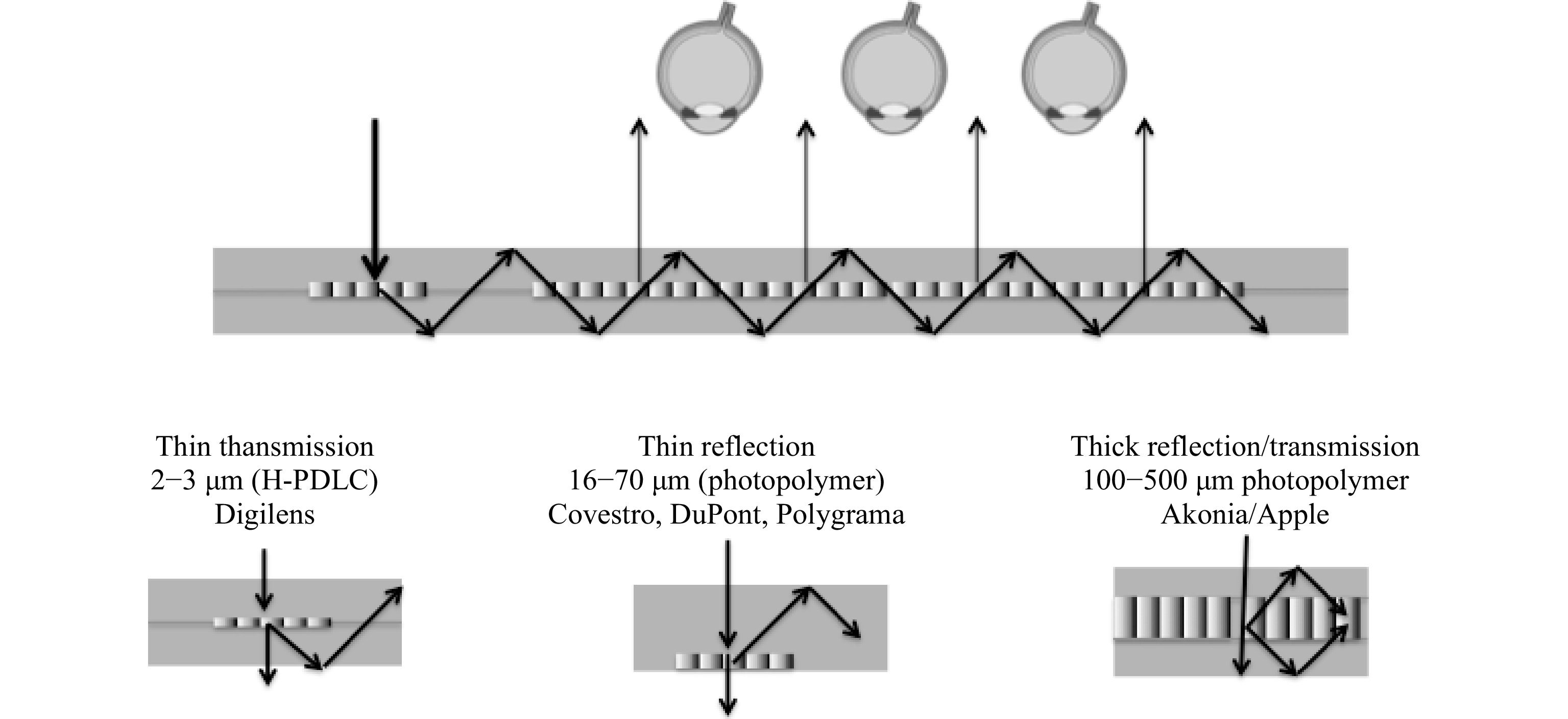
Fig. 16 Different types of volume holograms acting as in- and out-couplers in waveguide combiners.
A hologram sandwiched between plates might look more complex to produce than a reflective or transmission laminated version, but it has the advantage that it can operate in both transmission and reflection modes at the same time (for example, to increase the pupil replication diversity).
-
Fig. 17 reviews the various surface-relief gratings used in industry today (blazed, slanted, binary, multilevel, and analog), and how they can be integrated in waveguide combiners as in-coupling and out-coupling elements31-35.
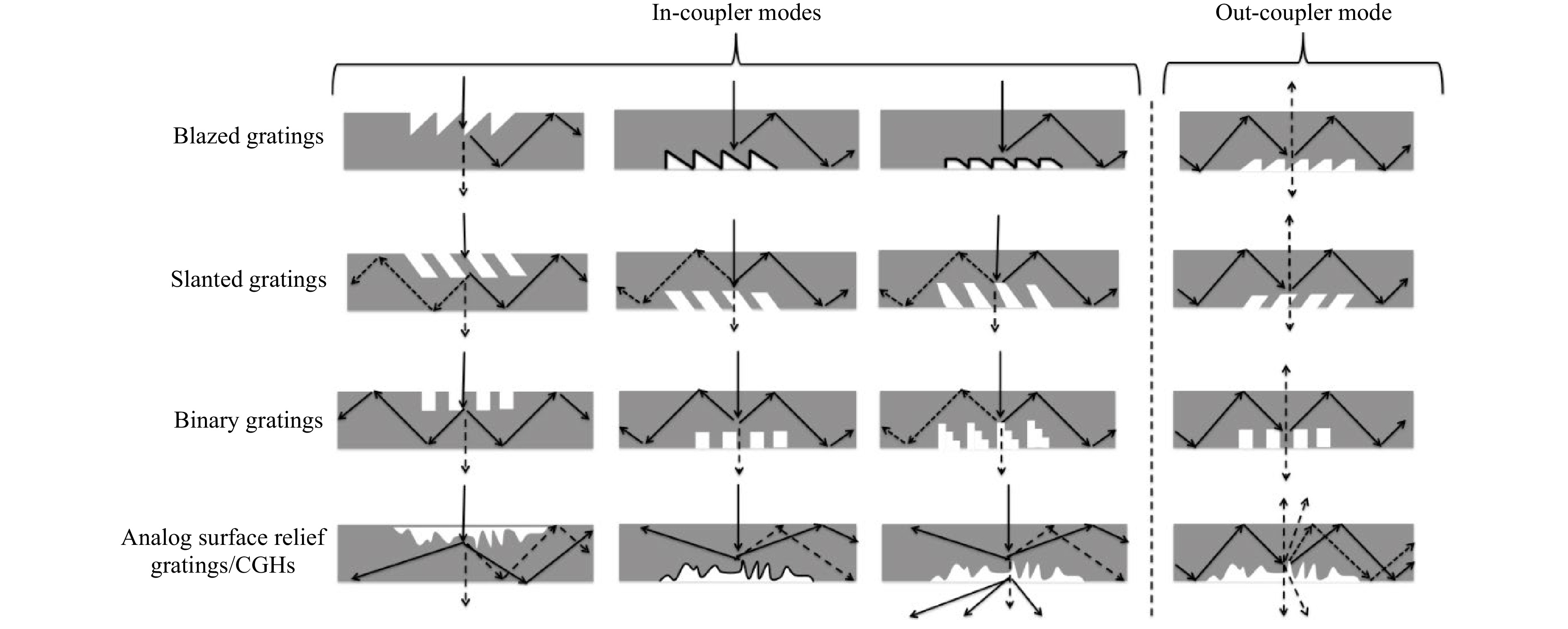
Fig. 17 Surface-relief grating types used as waveguide combiner in-couplers and out-coupler. Solid lines indicate reflective coatings on the grating surface, and dashed lines indicate diffracted orders.
Covering a surface-relief grating with a reflective metallic surface (see Fig. 17) will increase dramatically its efficiency in reflection mode. A transparent grating (no coating) can also work both in transmission and reflection modes, especially as an out-coupler, in which the field has a strong incident angle.
Increasing the number of phase levels from binary to quarternary or even eight or sixteen levels increases its efficiency as predicted by the scalar diffraction theory, for normal incidence. However, for a strong incidence angle and for small periods, this is no longer true. A strong out-coupling can thus be produced in either reflection or transmission mode.
Slanted gratings36,37 are very versatile elements and their spectral and angular bandwidths can be tuned by the slant angles. Front and back slant angles in a same period (or from period to period) can be carefully tuned to achieve the desired angular and spectral operation.
Surface relief gratings have been used as a commodity technology since mastering and mass replication techniques technologies were established and made available in the early 1990s. Typical periods for TIR grating couplers in the visible spectrum are below 500 nm, yielding nanostructures of just a few tens of nanometers if multilevel structures are required. This can be achieved by either direct e-beam write, i-line (or DUV) lithography, or even interference lithography (holographic resist exposure). Surface relief grating structures can be replicated in volumes by nano-imprint, a micro-lithography wafer fabrication technology developed originally for the IC industry38,39. Going from wafer-scale fabrication to panel-scale fabrication will reduce costs, allowing for consumer-grade AR and MR products.
Fig. 18 and Fig. 19 illustrate how some of the surface relief gratings shown in Fig. 17 have been applied to the latest waveguide combiners such as the Microsoft HoloLens 1 and Magic Leap One. Multilevel surface relief gratings have been used by companies such as Dispelix Oy, and quasi-analog surface relief CGHs have been used by others, such as WaveOptics Ltd (now part of Snap Inc).
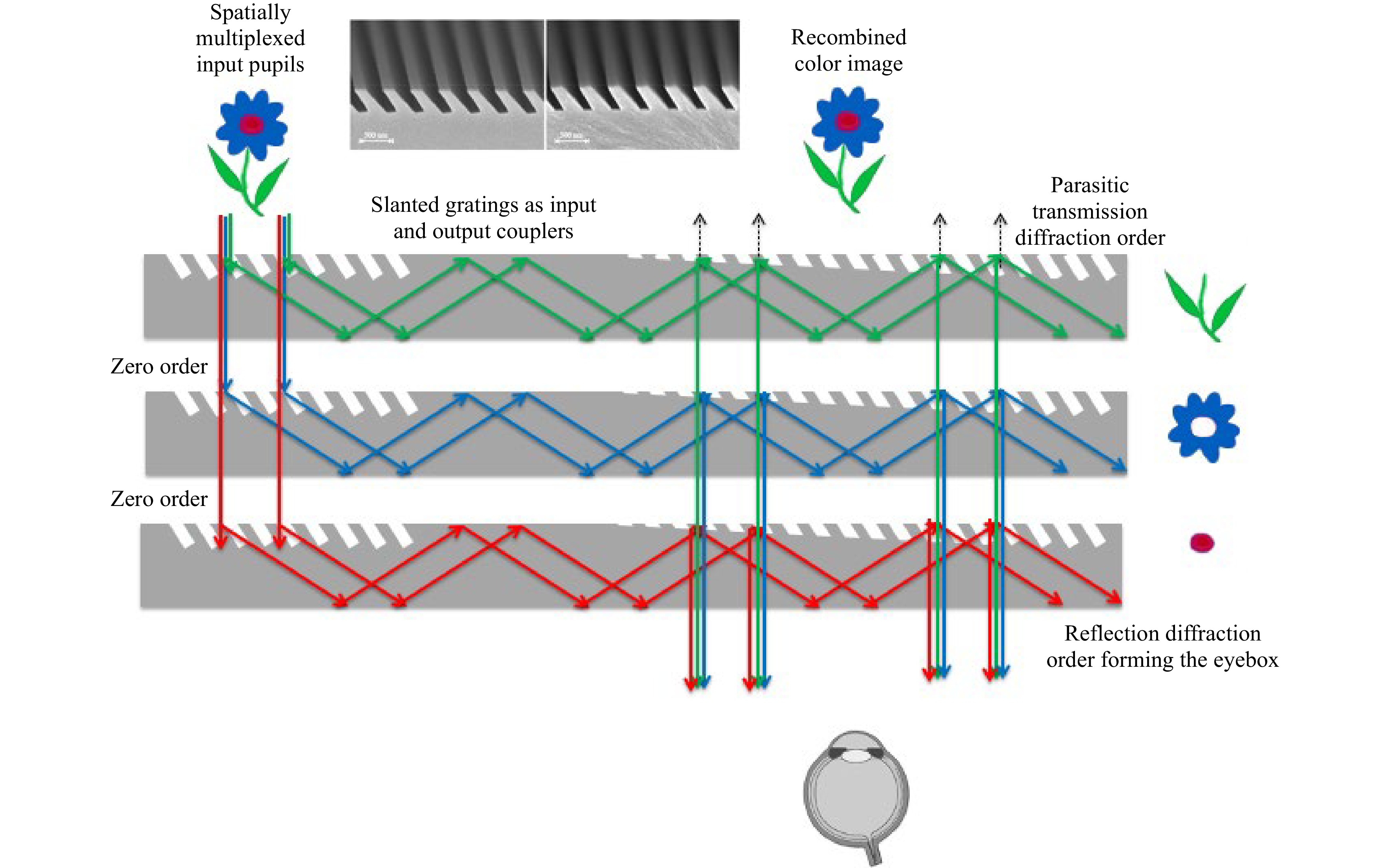
Fig. 18 Spatially color-multiplexed input pupils with slanted gratings as in- and out-couplers working in transmission and reflection mode (HoloLens 1 MR headset).
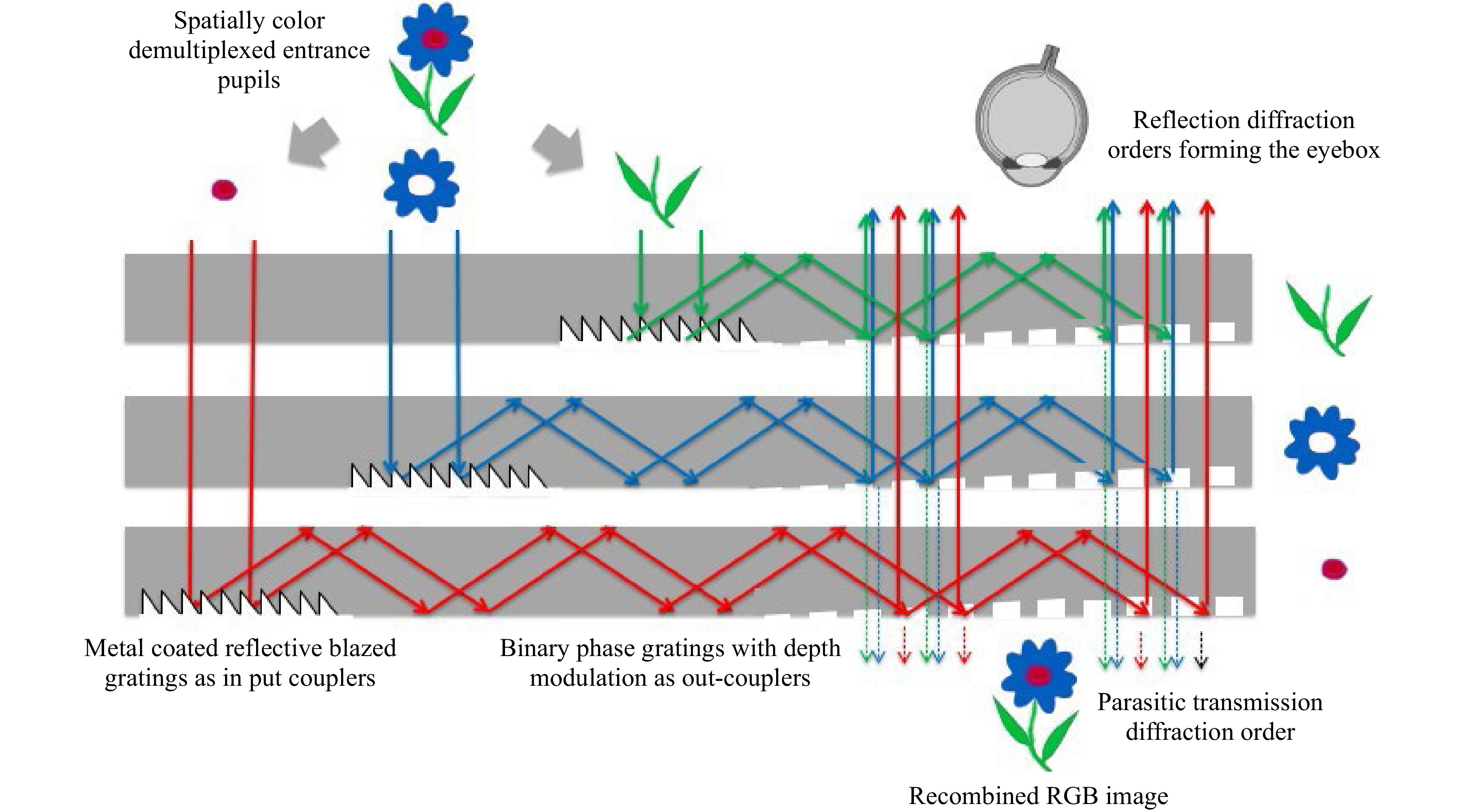
Fig. 19 Spatially color-de-multiplexed input pupils with 100% reflective blazed gratings as in-couplers and binary phase gratings as out-couplers (Magic Leap One MR headset).
Fig. 18 shows the waveguide combiner architecture used in the Microsoft HoloLens 1 MR headset (2015). The display engine is located on the opposite side of the eyebox. The single input pupil carries the entire image over the various colors at infinity (here, only two colors and the central field are depicted for clarity), as in a conventional digital projector architecture. The in-couplers have been chosen to be slanted gratings for their ability to act on a specific spectral range while letting the remaining spectrum unaffected in the zero order, to be processed by the next in-coupler area located on the guide below, and to do this for all three colors. Such uncoated slanted gratings work both in transmission and reflection modes but can be optimized to work more efficiently in a specific mode. The out-couplers here are also slanted gratings, which can be tuned to effectively work over a specific incoming angular range (TIR range) and leave the see-through field quasi-unaffected. The part of the see-through field that is indeed diffracted by the out-couplers is trapped by TIR and does not make it to the eyebox. These gratings are modulated in depth to provide a uniform eyebox to the user. Note the symmetric in- and out-coupler configuration compensating the spectral spread over the three LEDs bands.
The redirection gratings are not shown here. Input and output grating slants are set close to 45 deg and the redirection grating slants at half this angle. The periods of the gratings are tuned in each guide to produce the right TIR angle for the entire FOV for that specific color (thus the same central diffraction angle in each guide for each RGB LED color band).
Fig. 19 depicts the waveguide combiner architecture used in the Magic Leap One MR headset (2018). The display engine is located on the same side as the eyebox. The input pupils are spatially color-demultiplexed, carrying the entire FOV at infinity (here again, only two colors and the central field are depicted for clarity).
Today, typical yields for slanted gratings produced by Nano-Imprint Lithography (NIL) are typically in the 90% for indices lower than 1.8, for which the process is well defined. For refractive indices of 1.9 and 2.0, the yields are quite lower today. Various contract manufacturers are today using NIL equipment (EVG, Suss, Canon, etc…) to produce volume quantities of waveguides on either plates or wafers.
Spatial color de-multiplexing can be done conveniently with a color sequential LCoS display mode for which the illumination LEDs are also spatially de-multiplexed. In this configuration, the input grating couplers are strong blazed gratings, coated with a reflective metal (such as Al). They do not need to work over a specific single-color spectral width since the colors are already de-multiplexed. The out-couplers are simple top-down binary gratings, which are also depth modulated to produce a uniform eyebox for the user. These binary gratings are shallow, acting therefore very little on the see-through, but they have much stronger efficiency when working in internal reflection diffraction mode, since the optical path length in this case is longer by a factor of 2ncos(α) than in transmission mode, (where n is the index of the guide, and α is the angle if there is incidence in the guide). As in the HoloLens 1, most of the see-through field diffracted by the out-couplers is trapped by TIR.
The redirection gratings (not shown here) are also composed of binary top-down structures. The periods of the gratings are tuned in each guide to produce the right TIR angle for the entire FOV for that specific color (same central diffraction angles for each RGB LED color band).
Other companies use multilevel and/or quasi-analog surface relief diffractive structures to implement in- and out-couplers (see Fig. 17, Fig. 15). This choice is mainly driven by the complexity of the extraction gratings, acting both as redirection gratings and out-coupler gratings, making them therefore more complex than linear or slightly curved (powered) gratings, similar to iteratively optimized CGHs39. Allowing multilevel or quasi-analog surface relief diffractive structures increases the space bandwidth product of the element to allow more complex optical functionalities to be encoded with relatively high efficiency.
-
Resonant waveguide gratings (RWGs), also known as guided mode resonant (GMR) gratings or waveguide-mode resonant gratings40,41, are dielectric structures where these resonant diffractive elements benefit from lateral leaky guided modes. A broad range of optical effects are obtained using RWGs such as waveguide coupling, filtering, focusing, field enhancement and nonlinear effects, magneto-optical Kerr effect, or electromagnetically induced transparency. Thanks to their high degree of optical tuning (wavelength, phase, polarization, intensity) and the variety of fabrication processes and materials available, RWGs have been implemented in a broad scope of applications in research and industry. RWGs can therefore also be applied as in- and out-couplers for waveguide gratings42.
Fig. 20 shows an RWG on top of a lightguide (referred often incorrectly through the popular AR lingo as a “waveguide”), acting as the in- and out-couplers.
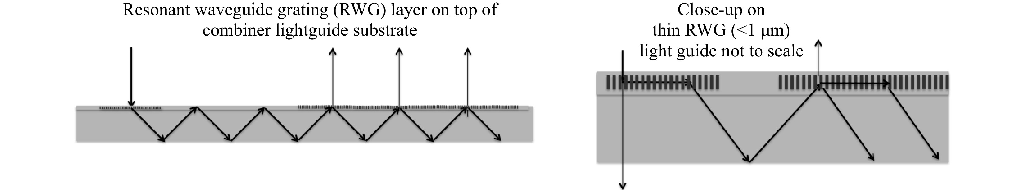
Fig. 20 Resonant Waveguide Gratings as in- and out-couplers on a waveguide combiner.
Roll-to-roll replication of such grating structures can help bring down overall waveguide combiner costs. The CSEM research center in Switzerland developed the RWG concept back in the 1980s, companies are now actively developing such technologies43.
-
Metasurfaces are a hot topic in research44: they can implement various optical element functionality in an ultra-flat form factor by imprinting a specific phase function over the incoming wavefront in reflection or transmission (or both) so that the resulting effect is refractive, reflective, or diffractive, or a combination of them. This phase imprint can be done through a traditional optical-path-difference phase jump or through Pancharatnam-Berry (PB) phase gratings/holograms.
Due to their large design space, low track length, and ability to render unconventional optical functions, metalenses could grow out of the lab to become a unique item in the engineer’s bag of tools. If one can implement in a fabricable metasurface an optical functionality that cannot be implemented by any other known optical element (diffractives, holographics, or Fresnels), it is particularly interesting. For example, having a true achromatic optical element is very desirable not only in imaging but also in many other tasks such as waveguide coupling. Another example is ultra-low track length focal stack for IR cameras from Metalenz Corp. Additionally, if one can simplify the fabrication and replication process by using metasurfaces, the design for manufacturing (DFM) can be compelling. However, optical efficiencies, design tools, and large scale fabrication will need to continue to improve and find their way into product.
-
Waveguide combiners could benefit greatly from a true achromatic coupler functionality: in- and/or out-coupling RGB FOVs, and matching each color FOV to the maximum angular range (FOV) dictated by the waveguide TIR condition. This would reduce the complexity of multiple waveguide stacks for RGB operation.
When it comes to implementing a waveguide coupler as a true achromatic grating coupler, one can either use embedded partial mirror arrays (as in the Lumus LOE combiner), design a complex hybrid refractive/diffractive prism array, or even record phase-multiplexed volume holograms in a single holographic material. However, in the first case, the 2D exit pupil expansion implementation remains complex, in the second case, the microstructures can get very complex and thick, and in the third case the diffraction efficiency can drop dramatically (as in the Konica Minolta or Sony RGB photopolymers combiners, or in the thick Akonia holographic dual photopolymer combiner, now part of Apple, Inc.).
It has been recently demonstrated in literature that metasurfaces can be engineered to provide a true achromatic behavior in a very thin surface with only binary nanostructures. It is easier to fabricate binary nanostructures than complex analog surface relief diffractives, and it is also easier to replicate them by nanoimprint lithography (NIL) or soft lithography and still implement a true analog diffraction function as a lens or a grating. The high index contrast required for such nanostructures can be generated by either direct imprint in high index inorganic spin-on glass or by NIL resist lift-off after an atomic layer deposition (ALD) process. Direct dry etching of nanostructured remains a costly option for a product.
It is important to remember that metasurfaces or thick volume holograms are not inherently achromatic elements, and never will be. However, when many narrow band diffraction effects are spatially or phase multiplexed in a metasurface or a thick volume hologram, their overall behavior over a much larger spectral bandwidth can effectively lead the viewer to think they are indeed achromatic: although each single hologram or metasurface operation are strongly dispersive, their cascaded contributions may result in a broadband operation which looks achromatic to the human eye (e.g. the remaining dispersion of each individual hologram or metasurface effect affecting a spectral spread that is below human visual acuity-one arcmin or smaller). It is also possible to phase multiplex surface relief holograms to produce achromatic effects, but more difficult than with thick volume holograms or thin metasurfaces.
Mirrors are of course perfect achromatic elements and will therefore produce the best polychromatic MTF (such as with Lumus LOE combiners or LetinAR pin mirror waveguides).
-
As we have reviewed in this section, world side leakage (also commonly referred to as “eye glow”) is a parasitic display feature that in some instances can block the eye contact when the display is on, and furthermore provide a very unnatural glow replacing the headset wearer’s eyes. Not all waveguides have same world side leakage. We classify in order the various waveguide combiner technologies below.
Waveguide technologies classification for world side leakage (and world side display rainbow effect):
- Surface relief gratings with binary profiles (about 50% of the eye side leakage).
- Surface relief gratings with slanted profiled (about 40% of the eye side leakage)
- Holographic grating couplers (about 8-10% of the eye side leakage).
- Reflective waveguides (5% without AR coating and <1% with AR coating)
-
Table 1 summarizes the various waveguide coupler technologies reviewed here, along with their specifics and limitations.
Waveguide
coupler techOperation Reflective coupling Transmission coupling Efficiency modulation Lensed out- coupler Spectral dispersion, Color uniformity Dynamically tunable Polarization maintaining Mass
productionCompany/
ProductEmbedded
mirrorsReflective Yes No Dielectric coatings No Minimal Good No Yes Slicing, coating, polishing, Lumus Ltd.
DK 50, Maximus 2D EPEMicro-prisms Reflective Yes No Dielectric coatings Yes Minimal Good No Yes Injection molding Optinvent. ORA Surface relief slanted grating Diffractive Yes Yes Depth, Duty cycle, slant Yes Strong Needs comp. Possible with LC No NIL (wafer, plate) Microsoft HoloLens, Vuzix Inc, Nokia,… Surface relief blazed grating Diffractive Yes No Blaze/antiblaze angles No Strong Needs comp. Possible with LC No NIL (wafer, plate) Magic Leap One, Surface relief binary grating Diffractive Yes Yes Depth, Duty cycle Yes Strong Needs comp. Possible with LC No NIL (wafer, plate) Magic Leap One Multilevel surface relief grating Diffractive Yes Yes Depth, Duty cycle Yes Strong Needs comp. Possible with LC Possible, but difficult NIL (wafer,plate) WaveOptics Ltd, BAE. Dispelix. Thin photopolymer hologram Diffractive Yes Yes Index swing Yes, but difficult Strong Needs comp. Possible with shear No Contact print roll to roll Sony Ltd, TruelifeOptics Ltd, H-PDLC volume holographic Diffractive No Yes Index swing Yes, but difficult Strong Need comp. Yes
(electrical)No Exposure Digilens Corp. (MonoHUD) Thick photopolymer hologram Diffractive Yes Yes Index swing Yes, but difficult Minimal Need com;. No No Multiple exposure Akonia Corp (now Apple Inc.) Resonant Waveguide Grating Diffractive Yes Yes Depth. Duty cycle Yes Can be mitigated NA Possible with LC Possible Roll to roll NIL CSEM / Resonannt Screens Metasurface coupler Mostly diffractive Yes Yes Various Yes Can be mitigated Needs comp. Possible with LC Possible NIL (wafer, plate) Metalenz Corp. Table 1. Benchmark of various waveguide coupler technologies.
Although this table shows a wide variety of optical couplers, most of today’s AR/MR/smart glass products are based on only a handful of traditional coupler technologies such as thin volume holograms, slanted surface-relief gratings, and embedded half-tone mirrors. The task of the optical designer (or rather the product program manager) is to choose the right balance and the best compromise between coupling efficiency, color uniformity over the eyebox and FOV, mass production costs, and size/weight.
Fig. 21 shows the various coupler elements and waveguide architectures grouped in a single table, including surface relief grating couplers, thin holographic couplers, and thick holographic couplers in three, two, and single flat guides. For geometric waveguide combiners that use embedded mirrors or other reflective/refractive couplers (such as micro-prisms).
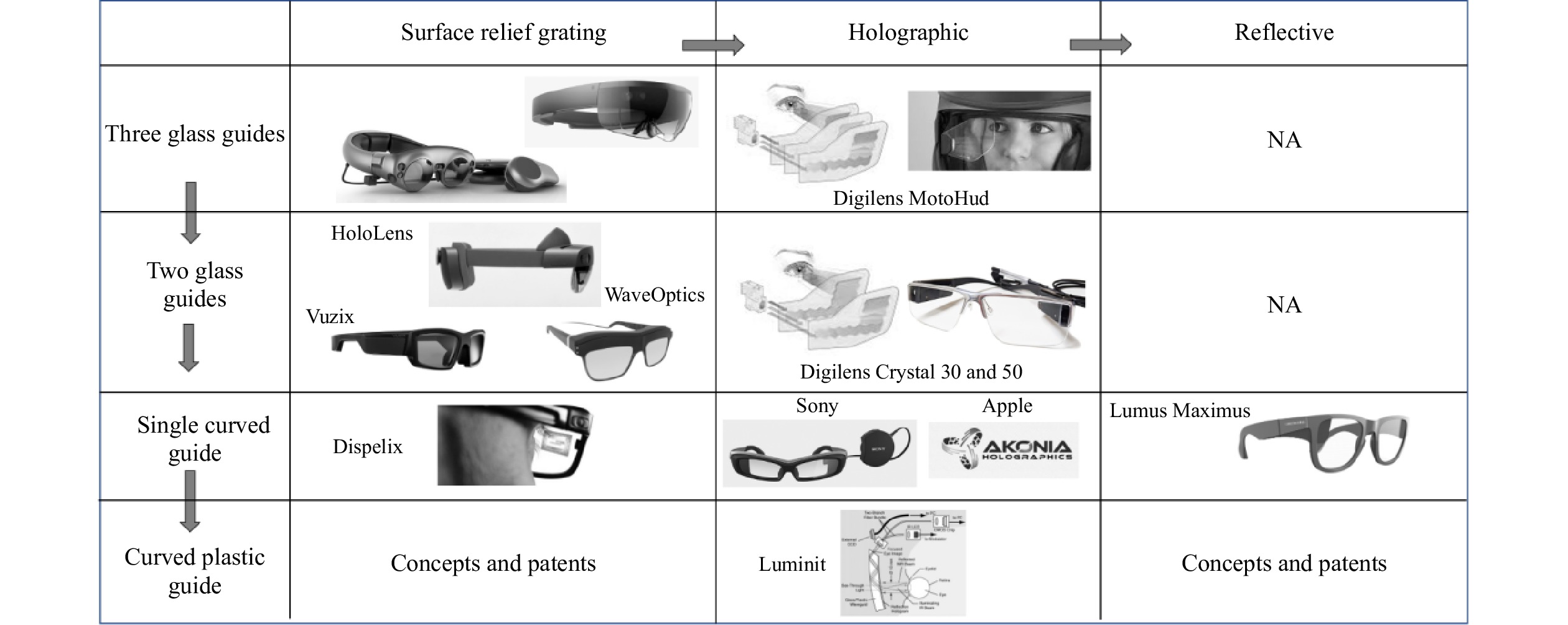
Fig. 21 Summary of waveguide combiner architectures with 1D or 2D EPE schemes.
-
Designing and modeling a waveguide combiner is very different from designing and modeling a freespace optical combiner. As conventional ray trace in standard optical CAD tools such as ZemaxTM, CodeVTM, FredTM or TraceProTM are sufficient to design effective free space and even TIR prism combiners, to design waveguide combiners, especially when using diffractive or holographic couplers, a hybrid ray-trace / rigorous Electro-Magnetic diffraction mode is usually necessary.
The modeling efforts is shared between two different tasks:
- Local, rigorous EM light interaction with micro- and anno-optics couplers (gratings, holograms, metasurfaces, RWGs, …)
- Global architecture design of the waveguide combiner, building up FOV, resolution, color and eyebox, by the use of more traditional ray trace algorithms.
-
Modeling of the angular and spectral Bragg selectivity of volume holograms, thin or thick, in reflection and transmission modes, can be performed with the couple wave theory developed by Kogelnik in 196929.
Similarly, modeling of the efficiency of surface relief gratings can be performed accurately with rigorous coupled-wave analysis (RCWA)33,34, especially the Fourier modal method (FMM). The finite difference time domain (FDTD) method—also a rigorous EM nanostructure modeling method—can in many cases be a more accurate modeling technique but also much heavier and more CPU time consuming. However, the FDTD will show all the diffracted fields, the polarization conversions, and the entire complex field, whereas the Kogelnik model and the RCWA will only give efficiency values for particular diffraction orders.
The FDTD can model non-periodic nanostructures, while RCWA can accurately model quasi-periodic structures. Thus, the FDTD might help with modeling k-vector variations (rolled k-vector) along the grating, slant, depths, and duty cycle variations, as well as random and systematic fabrication errors in the mastering and replication steps. The Kogelnik theory is best suited for slowly varying index modulations with moderate index swings (i.e., photopolymer volume holograms).
Free versions of the RCWA-FMM35 and FDTD32-35 codes can be found on the internet. Kogelnik theory can be easily implemented as a straightforward equation set for transmission and reflection modes. Commercial software suites implementing FDTD and RCWA are R-Soft from Synopsys and Lumerical.
These models predict the efficiency in each order for a single interaction of the light with the coupler element. In order to model the entire waveguide combiner, especially when a pupil replication scheme is used, conventional ray tracing optical design software can be used, such as Zemax, or more specific light-propagation software modules, such as the ones by LightTrans, Germany37 (see Fig. 22 for ray tracing through 2D EPE grating waveguides).
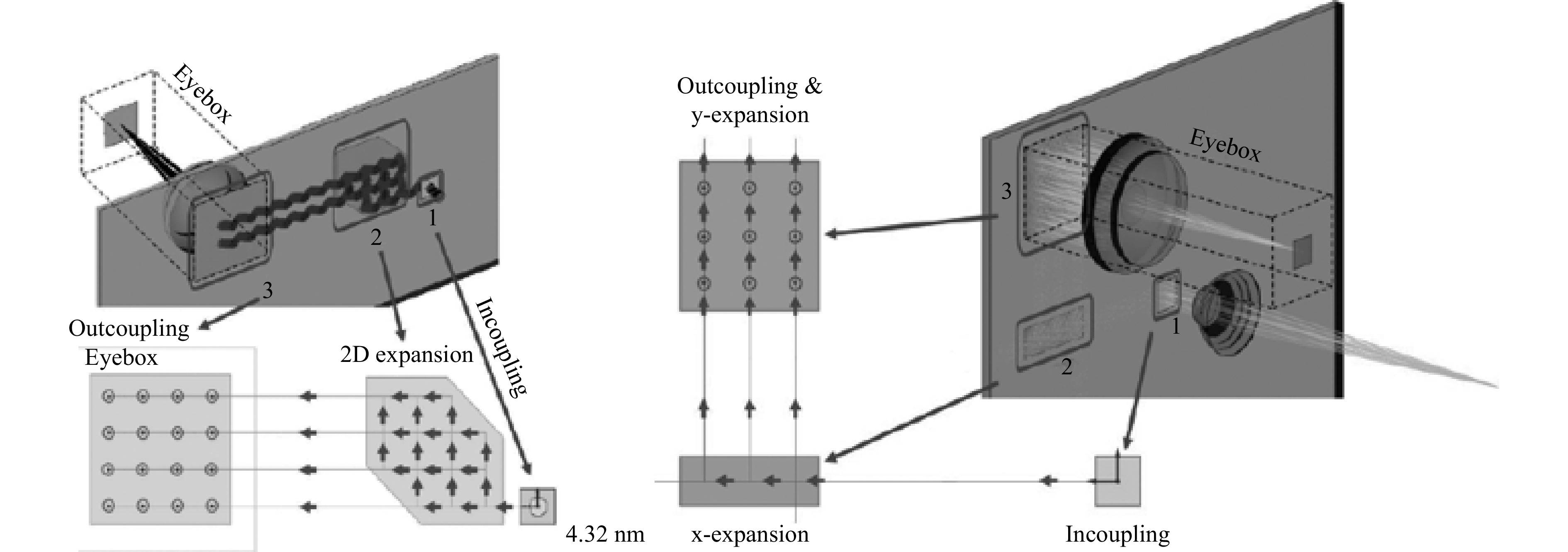
Fig. 22 Waveguide grating combiner modeling by LightTrans (Germany) in 2D EPE version.
The interaction of the EM field with the coupler regions (surface relief structures or index modulations) modeled through the RCWA or Kogelnik can be implemented via a dynamically linked library (DLL) in conventional optical design software based on ray tracing (e.g., C or Matlab code). As the FDTD numerical algorithm propagates the entire complex field rather than predicting only efficiency values (as in the RCWA or Kogelnik model), it is therefore more difficult to implement as a DLL.
Raytrace optimization of the high-level waveguide combiner architecture with accurate EM light/coupler interactions modeling are both required to design a combiner with good color uniformity over the FOV, a uniform eyebox over a target area at a desired eye relief, and high efficiency (in one or both polarizations). Inverse propagation from the eyebox to the optical engine exit pupil is a good way to simplify the optimization process. The design process can also make use of an iterative algorithm to optimize color over the FOV/eyebox and/or efficiency, or even reduce the space of the grating areas by making sure that no light gets lost outside the effective eyebox.
Waveguide couplers have specific angular and spectral bandwidths that affect both the FOV and the eyebox uniformity. A typical breakdown of the effects of a 2D EPE waveguide architecture on both spectral and angular bandwidths on the resulting immersive display is shown in Fig. 23.
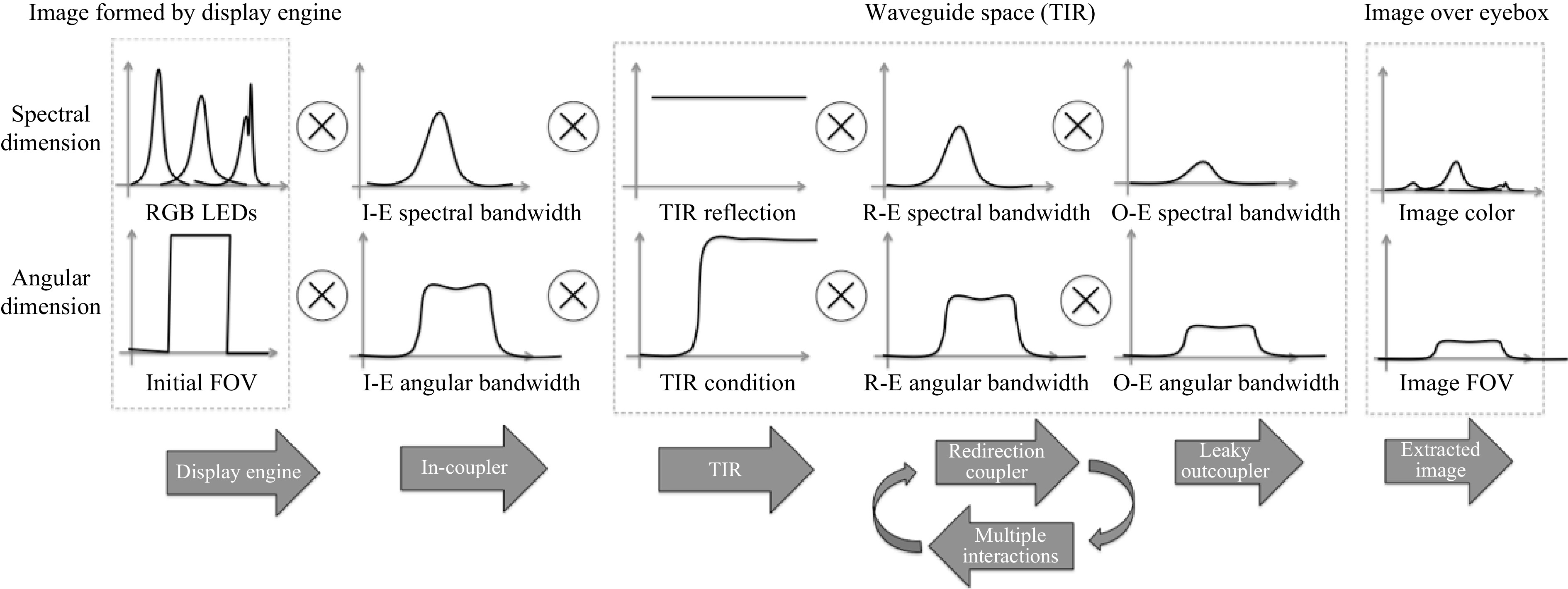
Fig. 23 Cascaded effects of the field/coupler interactions on the FOV uniformity.
Fig. 24 shows that the coupler’s spectral and angular bandwidths are critical to the FOV uniformity, especially color uniformity. While embedded mirrors and micro-prisms have a quasi-uniform effect on color and FOV, others do not, such as gratings and holograms. Therefore, it is interesting to have the flattest and widest spectral and angular bandwidths possible. For volume holograms, this means operating in reflection mode and having a strong index swing (Kogelnik), and for surface gratings, this means a high index (as predicted b the RCWA-FMM or FDTD). The angular bandwidth location can be tuned by the slant angle in both holograms and surface gratings. Multiplexing bandwidths can help to build a larger overall bandwidth, bot spectral and angular, and is used in various implementations today. Such multiplexing can be done in phase, in space or in time, or a combination of the above. Finally, as spectral and angular bandwidths are closely linked, altering the spectral input over the field can have a strong impact on FOV and vice versa.
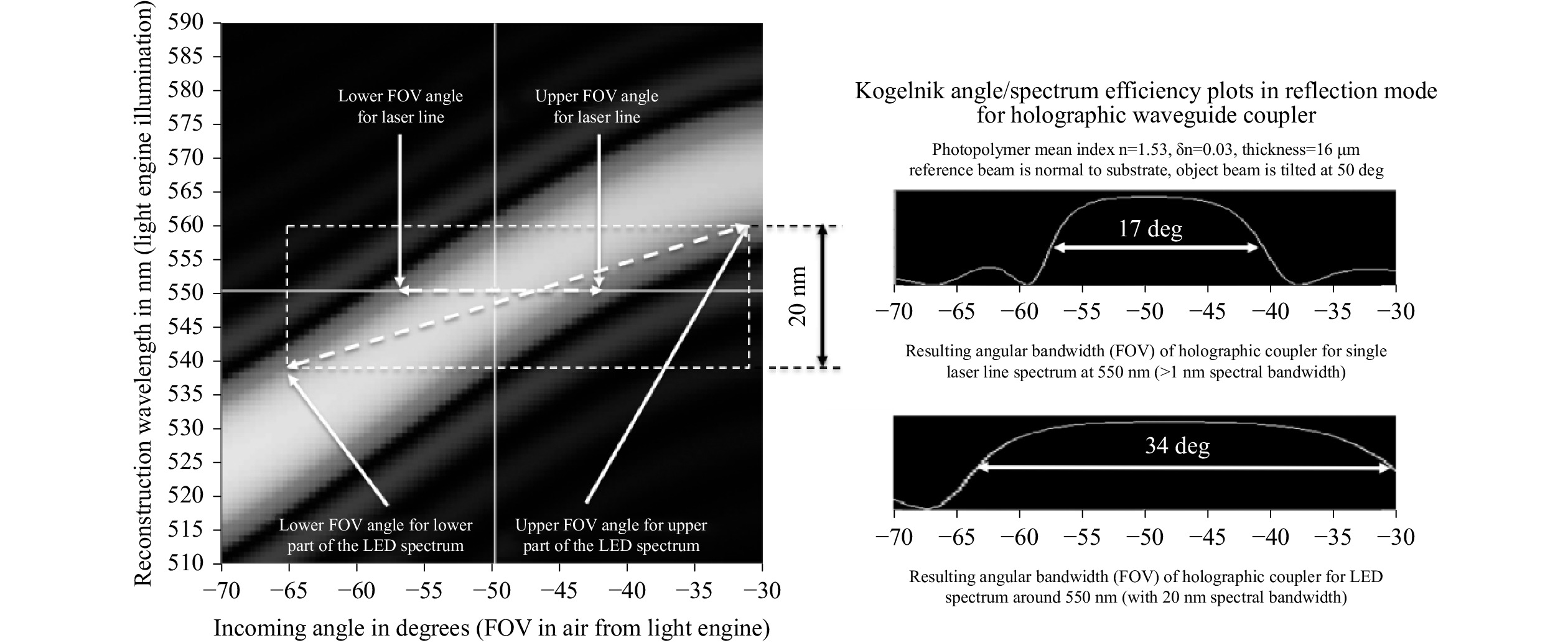
Fig. 24 Spectral source bandwidth building larger FOV (angular bandwidth) for photopolymer volume holographic coupler in waveguide combiners.
Polarization and degree of coherence are two other dimensions one should need to investigate especially when lasers or VCSELS are used in the optical engine or if polarization maintaining (or rather polarization conversion) is required. The multiple interactions in the R-E regions can produce multiple miniature Mach–Zehnder interferometers, which might modulate the intensity of the particular fields.
-
The ultimate task for a holographic or grating coupler is to provide the widest FOV coupling possible, matching the FOV limit dictated by the TIR condition in the underlying waveguide (linked to the refractive index of the waveguide material).
We have seen that volume holographic combiners have been used extensively to provide a decent angular in and out-coupling into the guide. However, most of the available holographic materials today have a low index swing and thus yield a relatively small angular bandwidth in the propagation direction. In this case the FOV bottleneck is the coupler, not the TIR condition in the waveguide.
A typical Kogelnik efficiency plot in the angular/spectral space for a reflection photopolymer volume holographic coupler is show in Fig. 24 (spectral dimension vertical and angular dimension horizontal).
The hologram specifications and exposure set-up in Fig. 24 are listed below:
- Mean holographic material index: 1.53,
- Holographic index swing: 0.03,
- Photopolymer thickness: 16 microns,
- Operation mode: reflective,
- Polarization: (‘s’ but very little change when moving to ‘p’ polarization),
- Design wavelength: 550 nm,
- Reconstruction wavelength: LED light from 540–560 nm (20-nm bandwidth),
- Normal incidence coupling angle: 50 deg in air.
When using a laser (<1-nm line) as a display source (such as in a laser MEMS display engine), the max FOV is the horizontal cross-section of the Kogelnik curved above (17-deg FWHM). However, when using the same color as an LED source (20 nm wide, such as in an LED-lit LCoS micro-display light engine, the resulting FOV is a slanted cross-section (in this case increased to 34-deg FWHM), and a 2× FOV gain is achieved without changing the waveguide index or the holographic coupler, only the illumination’s spectral characteristics.
However, this comes at the cost of color uniformity: the lower angles (left side of the FOV) will have more contributions from the shorter wavelengths (540 nm), and the higher angles (right side of the FOV) will have more contributions from the longer wavelengths (560 nm). This slight color non-uniformity over the FOV is typical for volume holographic couplers.
-
Unlike holographic couplers, which are originated and replicated by holographic interference in a phase change media (see previous section), surface-relief gratings (SRGs) are rather originated by traditional IC lithographic techniques and replicated by nano-imprint lithography (NIL) or soft lithography. The topological structure of the gratings can therefore be optimized digitally to achieve the best functionality in both spectral and angular dimensions. Topological optimization needs to account for DFM (design for manufacturing) and typical lithographic fabrication limitations. The angular bandwidth of an SRG coupler (i.e., the FOV that can be processed by this SRG) can be tuned by optimizing the various parameters of such a grating structure, such as the front and back slant angles, the grating fill factor, the potential coating(s), the grating depth, and of course the period of the grating (Fig. 25). Additional material variables are the refractive indices of the grating structure, grating base, grating coating, grating top layer, and underlying waveguide.
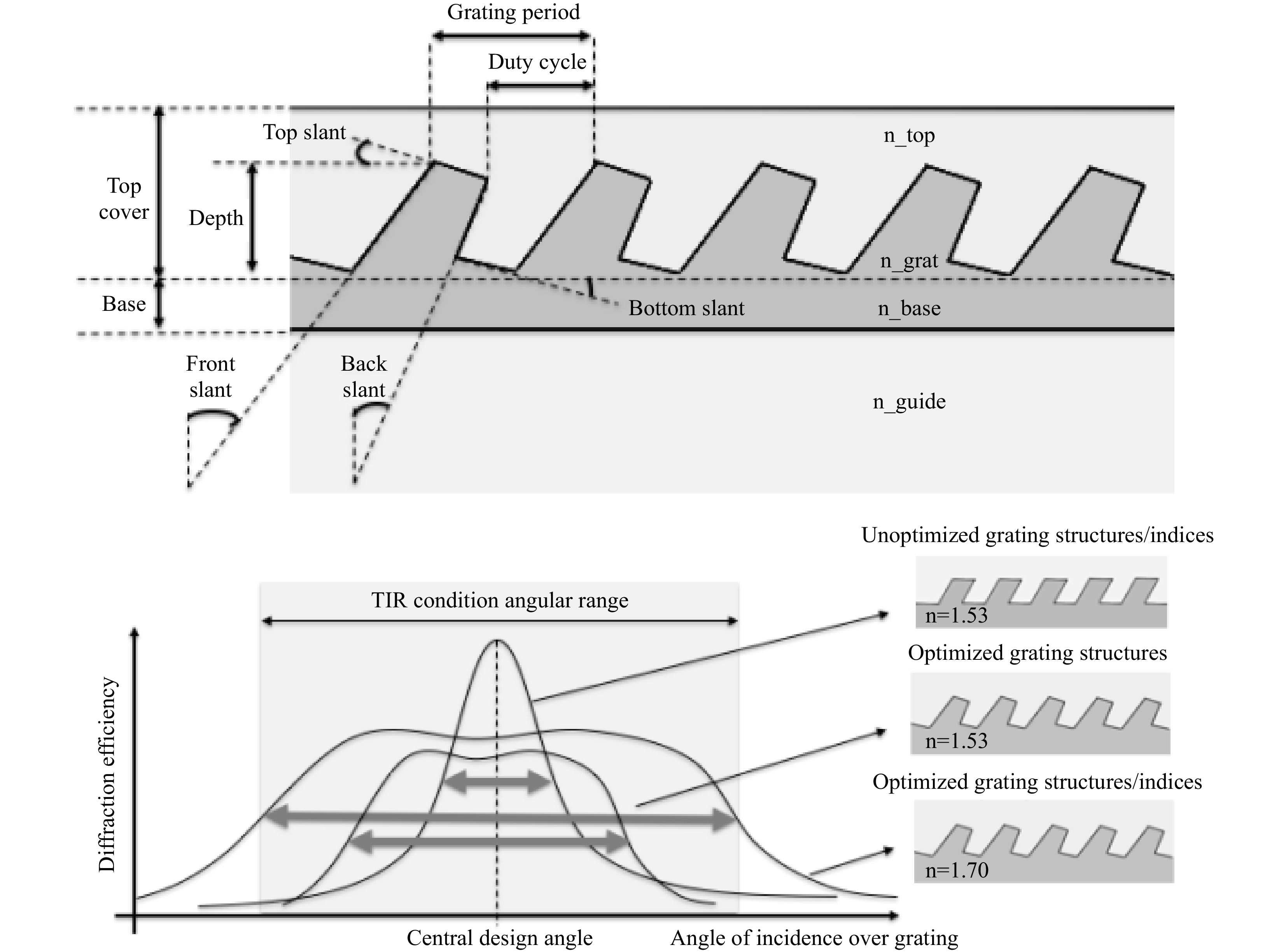
Fig. 25 Optimizing the grating parameters to optimize color uniformity over the FOV.
The SRG grating parameters can be optimized to provide a larger FOV, albeit with a lower overall efficiency, matching better the available angular bandwidth provided by the TIR condition in the guide. Lower efficiency is okay over the out-couplers since they are tuned in the low-efficiency range to produce a uniform eyebox (the in-coupler, however, needs to be highly efficient since there is only one grating interaction to couple the entire field into TIR mode).
Calculations of coupling efficiency have been carried out with an RCWA FMM algorithm and topological optimization by a steepest descent algorithm. Note that both unoptimized and optimized gratings have the same grating periods as well as the same central slant angle to position respectively the spectral and the angular bandwidths on identical system design points (with the FOV generated by the display engine and wavelength of the illumination source).
The bottleneck in FOV with the unoptimized grating structure is not the TIR condition (i.e., the index of the waveguide) but rather the grating geometry and the index of the grating. The angular bandwidth of the optimized grating should overlap the angular bandwidth of the waveguide TIR condition for best results over the largest possible FOV. Also, a “top hat” bandwidth makes the color uniformity over the FOV less sensitive to systematic and random fabrication errors in the mastering and the NIL replication of the gratings. Increasing the index of the grating and reducing the back slant while increasing the front slant angle can provide such an improvement.
Additional optimizations over a longer stretch of the grating can include depth modulations, slant modulations (rolling k-vector), or duty cycle modulations to produce an even wider bandwidth over a large, uniform eyebox.
-
Switchable or tunable TIR couplers can be used to optimize any waveguide combiner architecture, as in
- increasing the FOV by temporal sub-FOV stitching at double the refresh rate,
- increasing the brightness at the eye by steering a reduced size eyebox to the pupil position (thus increasing the perceived eyebox size), and
- increasing the compactness of the waveguide combiner by switching multiple single-color couplers in color sequence in a single guide.
Dynamic couplers can be integrated in various ways: polarization diversity with polarization-dependent couplers (the polarization switching occurring in the optical engine), reconfigurable surface acoustic wave (SAW) or acousto-optical modulator (AOM) couplers, electro-optical (EO) modulation of buried gratings, switchable surface-relief gratings in an LC layer, switchable metasurfaces in an multilayer LC layer, tunable volume holograms (by shearing, pressure, pulling), or switchable holographic-polymer dispersed liquid crystals (H-PDLC), as in Digilens’ volume holographic couplers.
-
The previous section discussed ways to model and optimize the performance of individual couplers, in either grating or holographic form. We now go a step further and look at how to design and optimize the overall waveguide combiner architectures.
-
We have seen that couplers can work in either transmission or reflection mode to create a more diverse exit-pupil replication scheme (producing a more uniform eyebox) or to improve the compactness of the waveguide by using both surfaces, front and back. The various couplers might direct the field in a single direction or in two or more directions, potentially increasing the FOV that can propagate in the waveguide without necessarily increasing its index.
Fig. 26 shows how the optical designer can expand the functionality of in- or out-couplers, with architectures ranging from bi-dimensional coupling to dual reflective/transmission operation in the same guide with sandwiched volume holograms or top/bottom grating couplers.
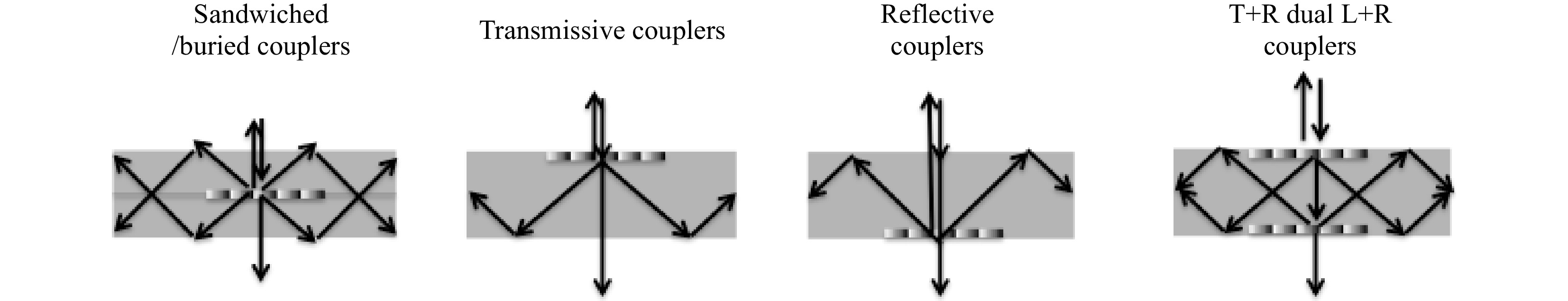
Fig. 26 More functional coupler architectures that yield compact and efficient waveguide combiners.
More complex and more functional coupler architectures have specific effects on MTF, efficiency, color uniformity, and FOV. For example, while the index of the guide allows for a larger FOV to propagate, the index of the grating structures in air would increase the spectral and angular bandwidths to process a larger FOV without compromising color uniformity or efficiency. The waviness of the waveguide itself will impact the MTF as random cylindrical powers added to the field. Multiple stacked waveguides might be efficient at processing single colors, but their misalignment will impact the MTF as misaligned color frames. Similarly, hybrid top/bottom couplers will affect the MTF if they are not perfectly aligned (angular alignment within a few arc seconds).
-
As the TIR field gets depleted when the image gets extracted along the out-coupler region, the extraction efficiency of the out-coupler needs to gradually increase in the propagation direction to produce a uniform eyebox. This complicates the fabrication process of the couplers, especially when the gradual increase in efficiency needs to happen in both pupil replication directions.
For volume holograms, the efficiency can be increased by a stronger index swing in the photopolymer or PDLC (through a longer exposure or a thickness modulation). For surface relief gratings, there are a few options, as shown in Fig. 27. This is true for the redirection grating (R-E) as well as the out-coupler (O-E).
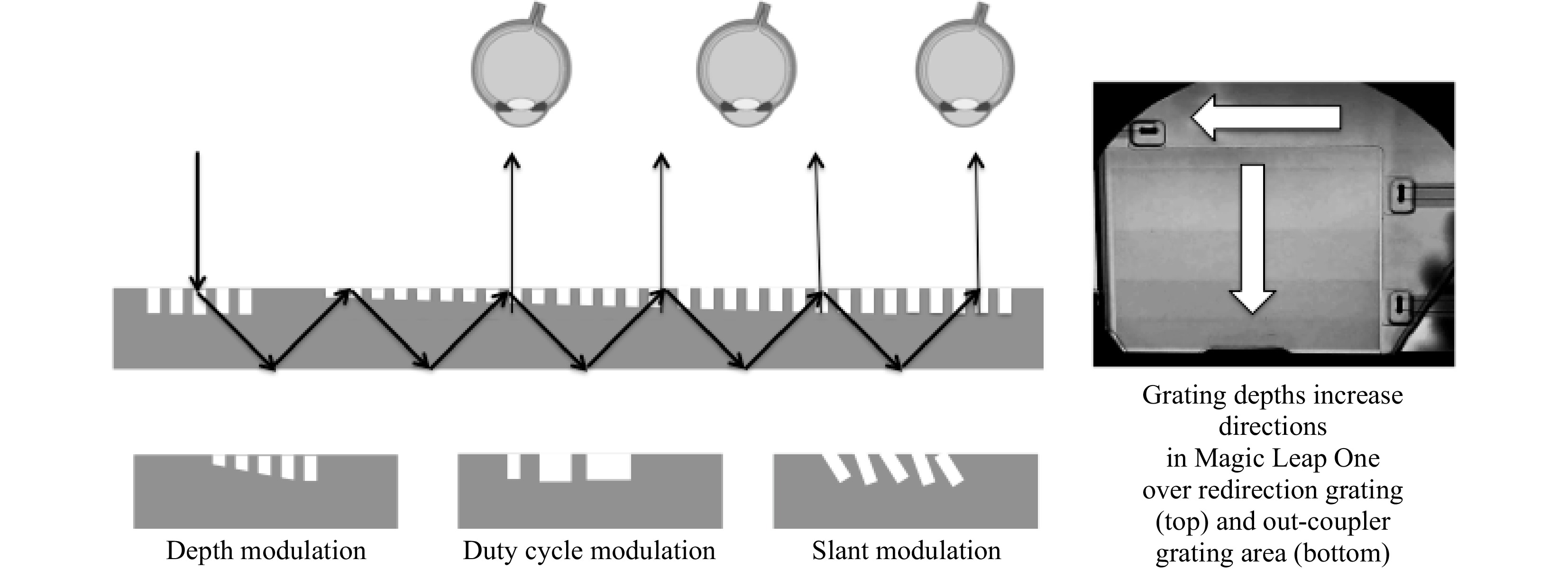
Fig. 27 Modulation of the outcoupling efficiency to build up a uniform eyebox.
Groove depth and duty cycle modulation can be performed on all type of gratings, binary, multilevel, blazed, and slanted. Duty cycle modulation has the advantage of modulating only the lateral structures, not the depth, which makes it an easier mastering process. Modulating the depth of the gratings can be done in binary steps (as in the Magic Leap One, Fig. 28– right) or in a continuous way (Digilens waveguide combiners).
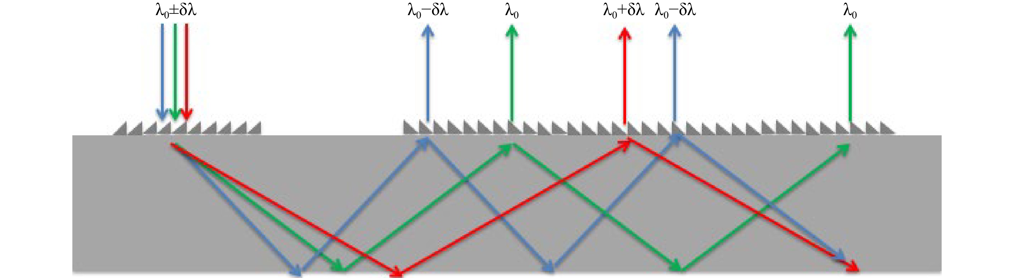
Fig. 28 Spectral spread compensation in a symmetric in-coupler/out-coupler waveguide combiner.
Grating front- and back-slant angle modulation (in a single grating period or over a larger grating length) can change the angular and spectral bandwidths to modulate efficiency and other aspects of the coupling (angular, spectral, polarization). Periodic modulation of the slant angles is sometimes also called the “rolling k-vector” technique and can allow for larger FOV processing due to specific angular bandwidth management over the grating area. Once the master has been fabricated with the correct nanostructure modulation, the NIL replication process of the gratings is the same no matter the complexity of the nanostructures (caution is warranted for slanted gratings where the NIL process must resolve the undercut structures; however, the slanted grating NIL process (with slants up to 50 deg) has been mastered by many foundries around the world)37.
-
Spectral spread comes to mind as soon as one speaks about gratings or holographic elements. It was the first and still it is the main application pool for gratings and holograms: spectroscopy. Spectral spread is especially critical when the display illumination is broadband, such as with LEDs (as in most of the waveguide grating combiner devices today, such as the HoloLens 1, Vuzix, Magic Leap, Digilens, Nokia, etc.), with a notable difference in the HoloLens 2 (laser MEMS display engine). The straightforward technique to compensate for the inevitable spectral spread is to use a symmetric in-coupler/out-coupler configuration, in which the gratings or holograms work in opposite direction and thus compensate in the out-coupler any spectral spread impacted in the in-coupler (Fig. 28).
Although the spectral spread might be compensated, one can notice on Fig. 28 that the individual spectral bands are spatially de-multiplexed at the exit ports while multiplexed at the entry port. Strong exit-pupil replication diversity is thus required to smooth out any color non-uniformities generated over the eyebox.
This symmetric technique might not be used to compensate for spectral spread across different colors (RGB LEDs) but rather for the spread around a single LED color. The spread across colors might stretch the RGB exit pupils too far apart and reduce the FOV over which all RGB colors can propagate by TIR.
The pupil replication diversity can also be increased by introducing a partial reflective layer in the waveguide (by combining two plates with a reflective surface), thus producing a more uniform eyebox in color and field.
-
The different fields propagating by TIR down the guide are also spread out, no matter the coupler technology (mirrors, prisms, gratings, holograms, etc.), see Fig. 29.
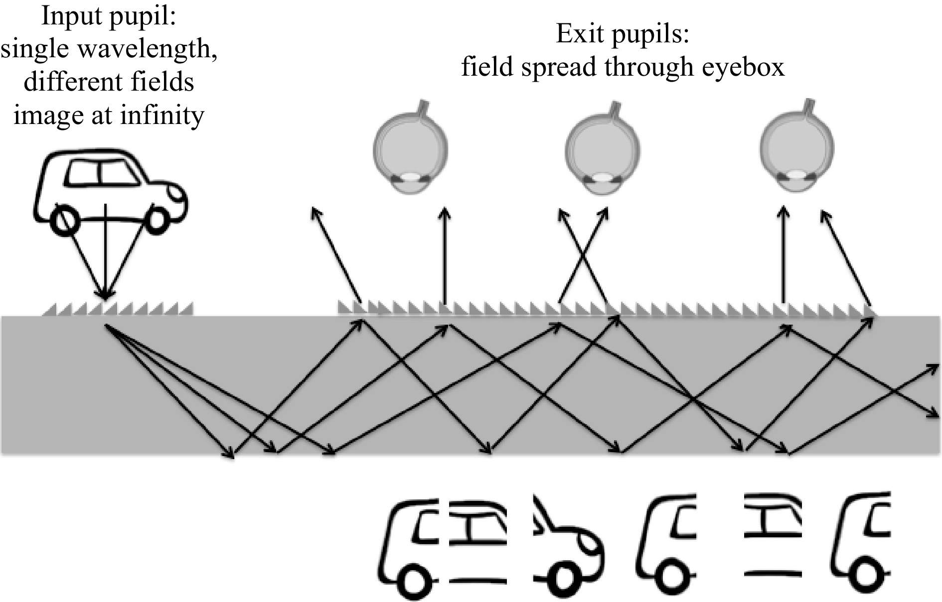
Fig. 29 Fractional field spread in a waveguide combiner.
A uniform FOV (i.e., all fields appearing) can be formed over the eyebox with a strong exit pupil diversity scheme. This is a concept often misunderstood as in many cases only one field is represented when schematizing a waveguide combiner. Fig. 29 shows the field spread occurring in a diffractive waveguide combiner. The number of replicated fields is also contingent on the size of the human eye pupil. If the ambient light gets bright, i.e., the human eye pupil gets smaller, then only part of the FOV might appear to the user, missing a few fields.
-
When a pupil replication scheme is used in a waveguide combiner, no matter the coupler, the input pupil needs to be formed over a collimated field (image at infinity/far field). If the focus is set to the near field instead of the far field in the display engine, each waveguide exit pupil will produce an image at a slightly different distance, thereby producing a mixed visual experience, overlapping the same image with different focal depths. It is quasi-impossible to compensate for such focus shift over the exit pupils because of both spectral spread and field spread over the exit pupils, as discussed previously. Fig. 30 shows such a focus spread over the eyebox from an input pupil over which the image is formed in the near field.
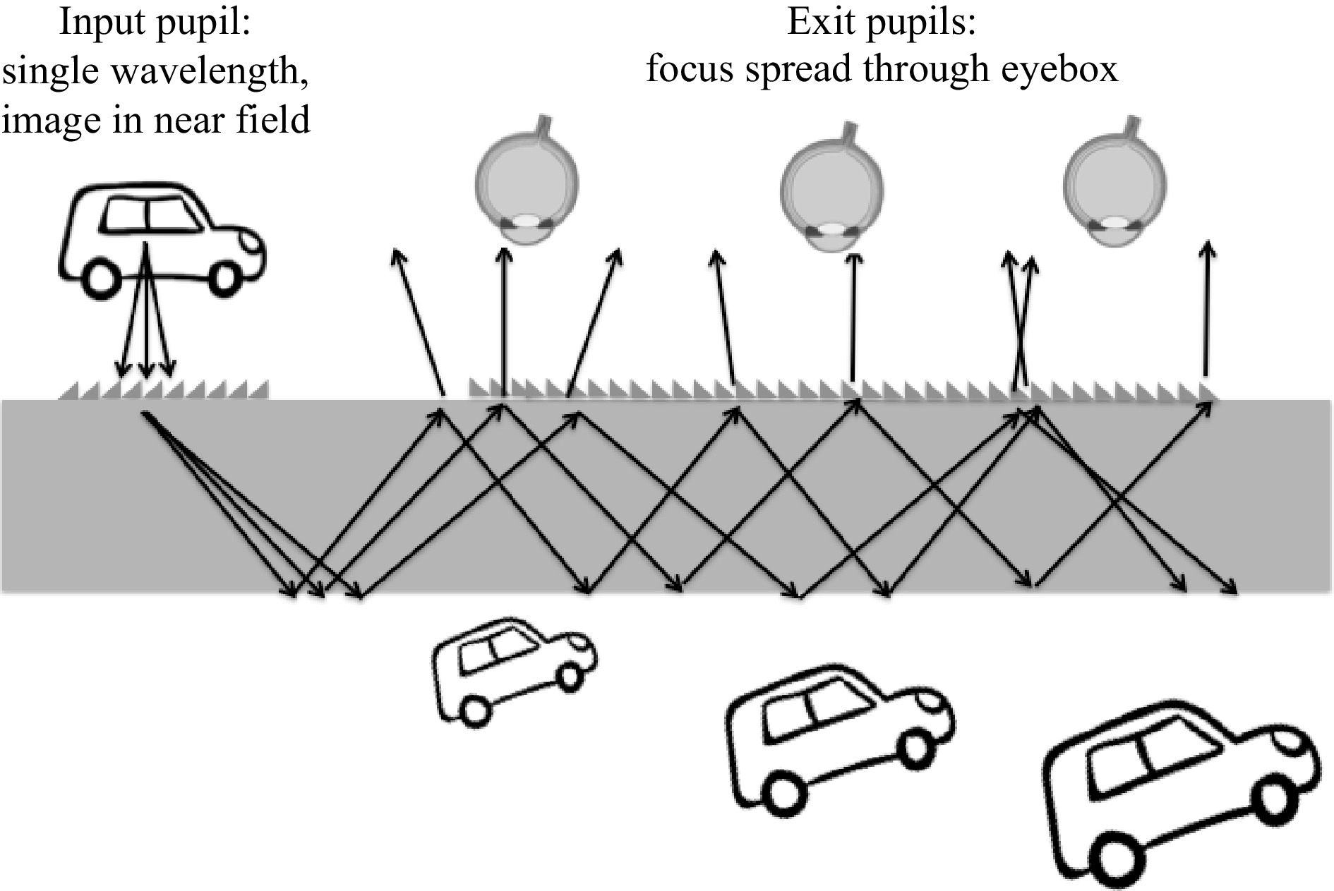
Fig. 30 Focus spread in a waveguide combiner with a non-collimated input field.
The image over the input pupil can, however, be located in the near field when no pupil replication scheme is performed in the guide, such as in the Epson Moverio BT300 or in the Zeiss “Tooz” Smart Glass (yielding a small FOV and small eyebox).
When pupil replication is used in the guide, the virtual image can be set at a closer distance for better visual comfort by using a static (or even tunable) negative lens acting over the entire eyebox. For an unperturbed see-through experience, such a lens needs to be compensated by its conjugate placed on the world side of the combiner waveguide. This is the architecture used in the Microsoft HoloLens 1 (2015)37.
Another, more compact way would introduce a slight optical power in the O-E, so that this coupler takes the functionality of an off-axis lens (or an off-axis diffractive lens) rather than a simple linear grating extractor or linear mirror/prism array. Although this is difficult to implement with a mirror array (as in an LOE), it is fairly easy to implement with a grating or holographic coupler. The grating lens power does not affect the zeroth diffraction order that travels by TIR down the guide but affects only the out-coupled (or diffracted) field. The see-through field is also not affected by such a lensed out-coupler since the see-through field diffracted by such an element would be trapped by TIR and thus not enter the eye pupil of the user.
All three configurations (no lens for image at infinity, static lens with its compensator, and powered O-E grating) are shown in Fig. 31. The left part of the eyebox shows an extracted field with image at infinity, the center part shows an extracted field with image at infinity that passes through a negative lens to form a virtual image closer to the user and its counterpart positive lens to compensate for see-through (as in the Microsoft HoloLens 1, 2015), and the right part of the eyebox shows an extracted field with the image directly located in the near field through a powered grating extractor (as with an off-axis diffractive lens, e.g., the Magic Leap One, 2018).
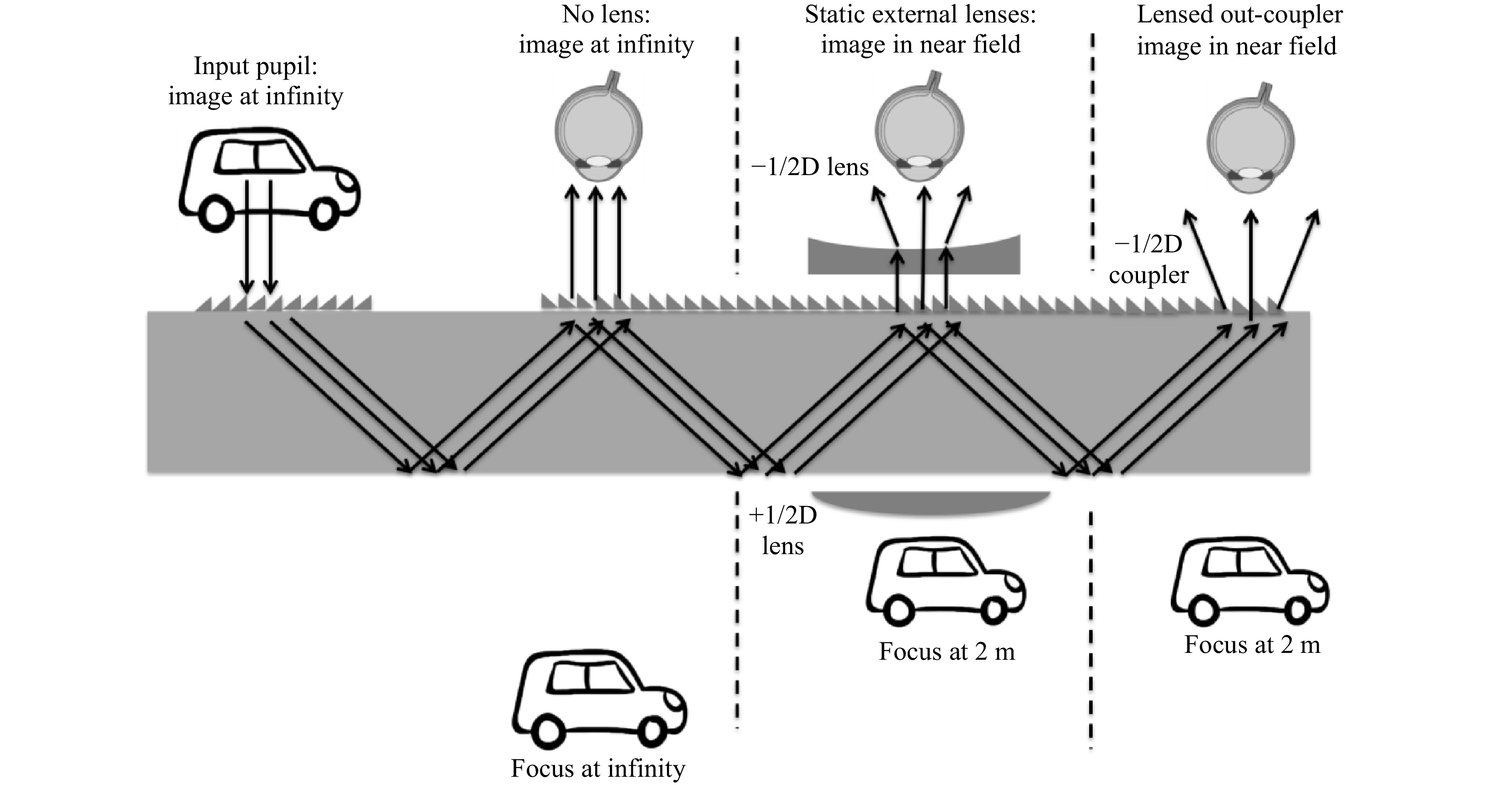
Fig. 31 Two out-coupler architectures positioning the virtual image in the near field over all exit pupils.
For example, a half-diopter negative lens power would position the original extracted far field image to a more comfortable 2-m distance, uniformly over the entire eyebox.
A powered out-coupler grating might reduce the MTF of the image, especially in the direction of the lens offset (direction of TIR propagation), since the input (I-E) and output (O-E) couplers are no more perfectly symmetric (the input coupler being a linear grating in both cases, and the out-coupler an off-axis diffractive lens). Thus, the spectral spread of the image in each color band cannot be compensated perfectly and will produce LCA in the direction of the lens offset. This can be critical when using an LED as an illumination source, but it would affect the MTF much less when using narrower spectral sources, such as lasers or VCSELs.
One of the main problems with such a lensed out-coupler grating configuration when attempting to propagate two colors in the same guide (for example, a two-guide RGB waveguide architecture is the generation of longitudinal chromatic aberrations (due to the focus changing with color since the lens is diffractive). Using a single color per guide and a laser source can greatly simplify the design task.
-
We have seen in the previous paragraphs that the spectral spread of grating and holographic couplers can be perfectly compensated with a symmetric in- and out-coupler configuration. This is possible over a single color band but will considerably reduce the FOV if used over the various color bands (assuming that the couplers will work over these various spectral bands).
In order to maximize the RGB FOV in a waveguide combiner, one solution is to use stacked guides optimized each for a single color band (see Fig. 32), each coupling a maximum FOV by tuning the diffraction angle of the in- and out-couplers accordingly. This is the architecture used in both HoloLens 1 and Magic Leap One although the position of the input pupil (light engine) is opposite in both devices.
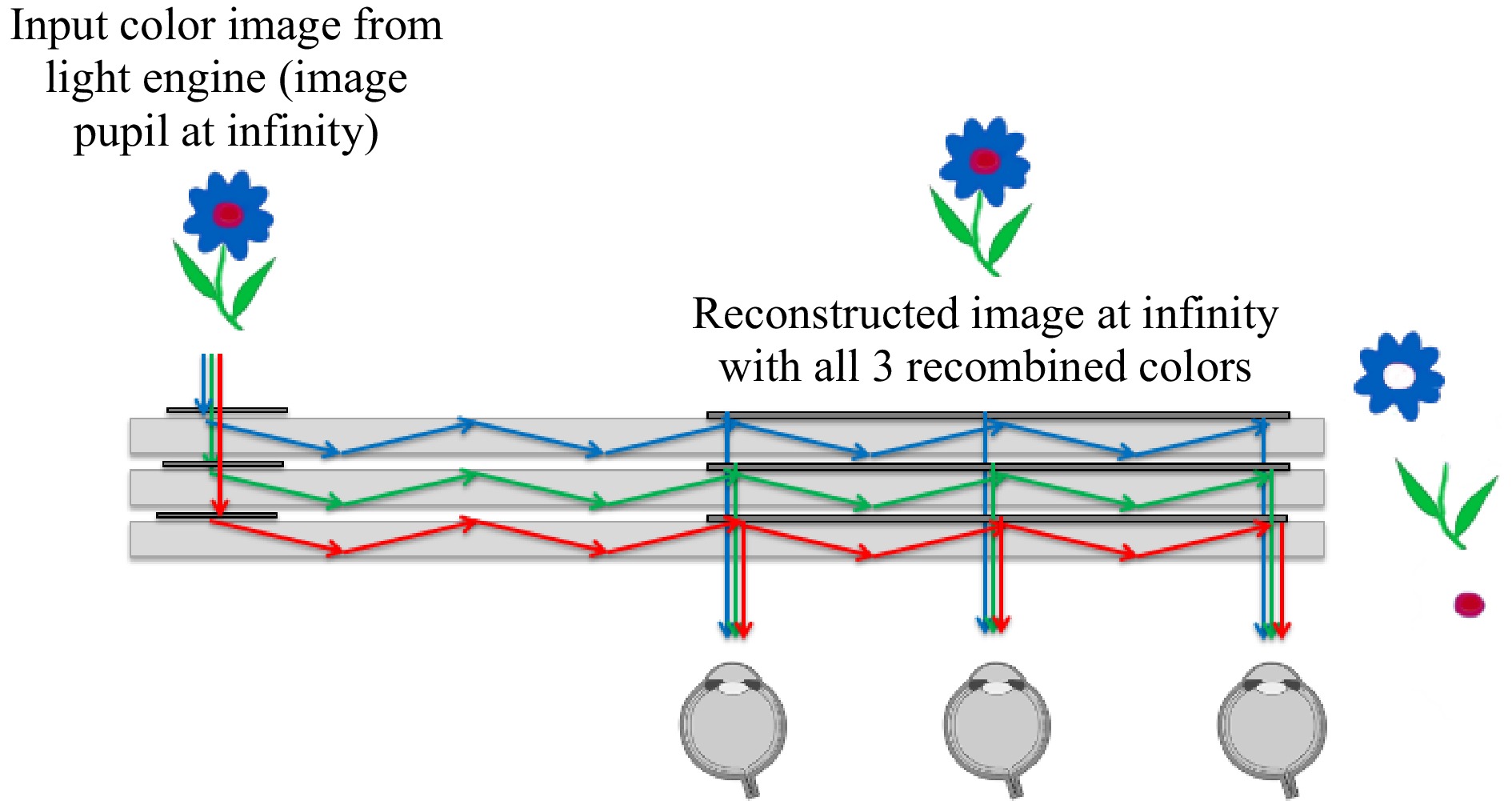
Fig. 32 Stacked waveguides combiners that provide the largest FOV TIR propagation over three colors.
Air gaps between all plates are required to produce the TIR condition. Such gaps also allow for additional potential filtering in between plates for enhanced performance (such as spectral and polarization filtering).
Fig. 33 shows the functional diagram of such a single-color plate as a top view as well as its k-vector space depiction. Here again, I-E refers to the in-coupler, R-E refers to the leaky 90-deg redirection element, and O-E refers to the leaky out-coupler that forms the final eyebox (for 2D pupil replications).
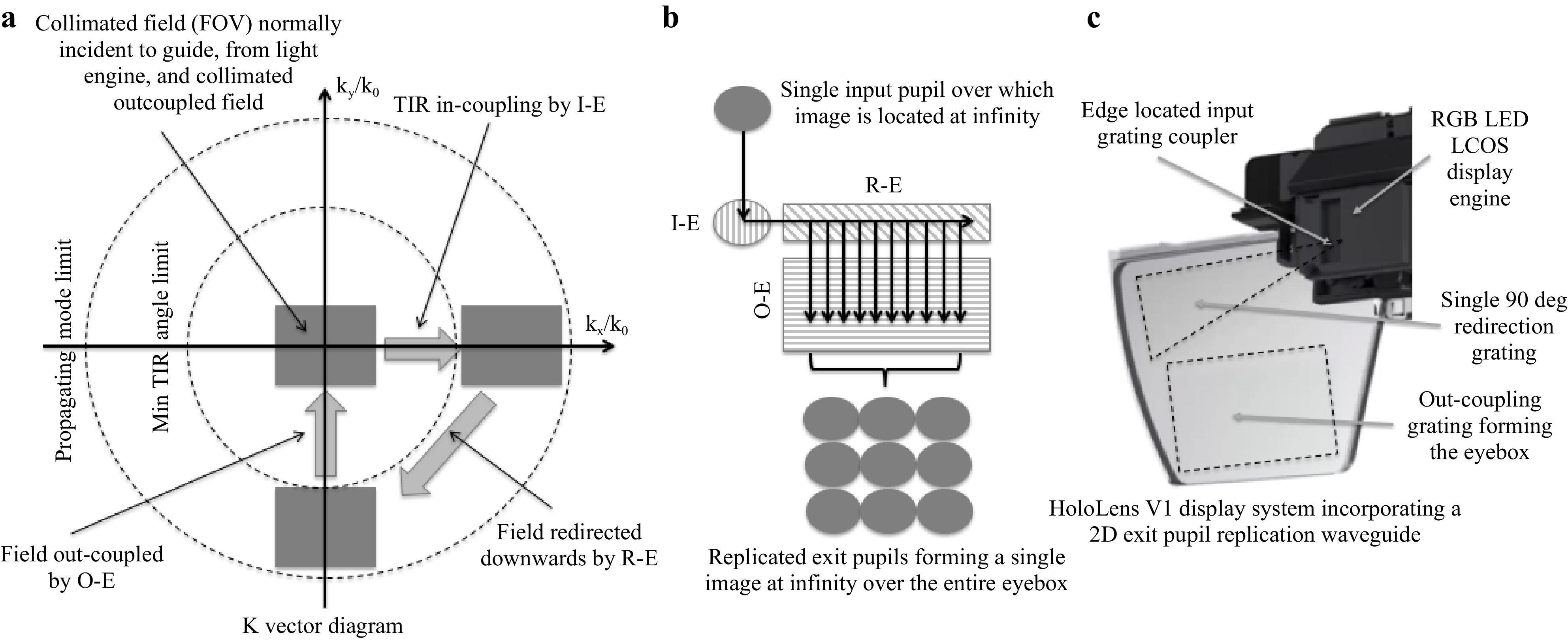
Fig. 33 k-vector diagram and lateral pupil replication layout for a single guide and single color.
Note that the entire FOV is shown on the k-vector diagram, but only a single field (central pixel in the FOV, with entry normal to the guide) is shown in the eyebox expansion schematic..
The FOV in the direction of the in-coupling can be increased by a factor of two when using a symmetric in-coupling configuration44 in which the input grating or hologram (or even prism(s)) would attempt to couple the entire FOV to both sides.
As the TIR angular range does not support such an enlarged FOV, part of the FOV is coupled to the right and part of the FOV is coupled to the left. Due to the opposite directions, opposite sides of the FOV travel in each direction. If such TIR fields are then joined back with a single out-coupler, the original FOV can be reconstructed by overlapping both partial FOVs, as in Fig. 34.
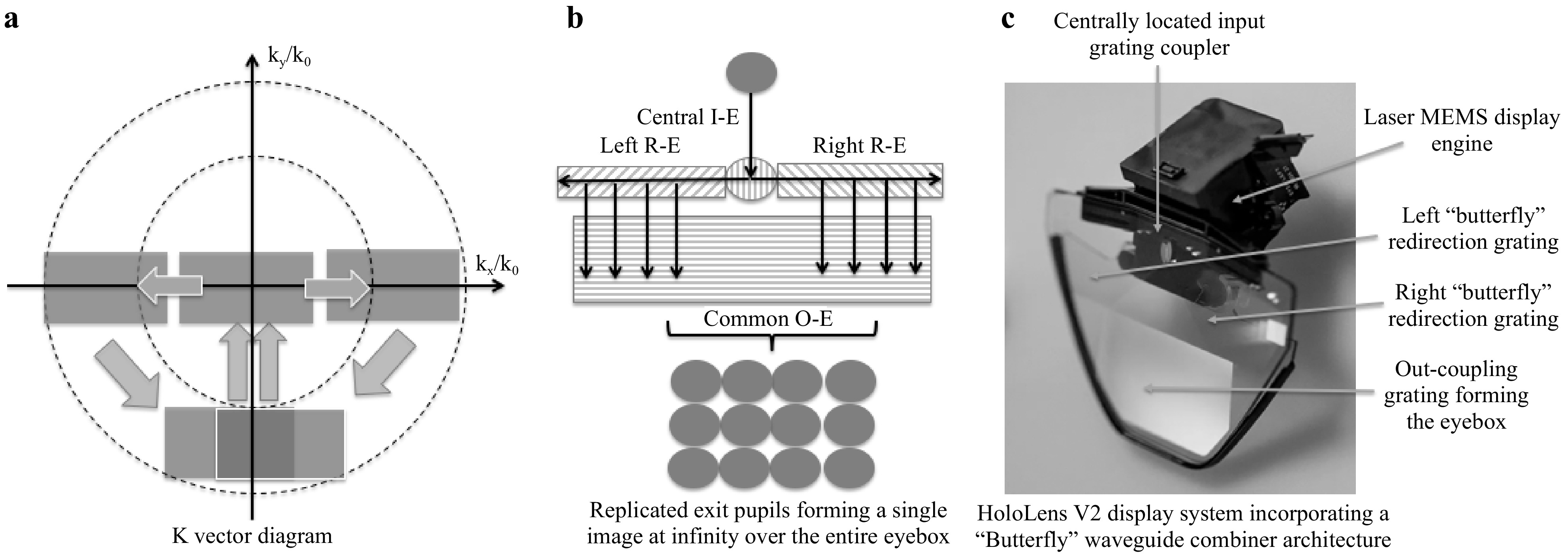
Fig. 34 Symmetric in-coupling for FOV increase in the direction of in-coupling.
In the orthogonal direction, the FOV that can be coupled by TIR remains unchanged. This concept can be taken to more than one dimension, but the coupler space on the waveguide can become prohibitive.
-
We have reviewed the various coupler technologies that can be used in waveguide combiners, as well as the 2D exit pupil expansion that can be performed in waveguide combiners. Waveguide combiners are desirable since their thickness is not impacted by the FOV, unlike other combiner architectures such as free-space or TIR prisms. However, the lateral dimensions of the waveguide (especially the redirection coupler and out-coupler areas over the waveguide) are closely linked to size of the in-coupled FOV, as shown in Fig. 35. For example, the R-E region geometry is dictated by the FOV in the waveguide medium: it expands in the direction orthogonal to the TIR propagation, forming a conical shape.
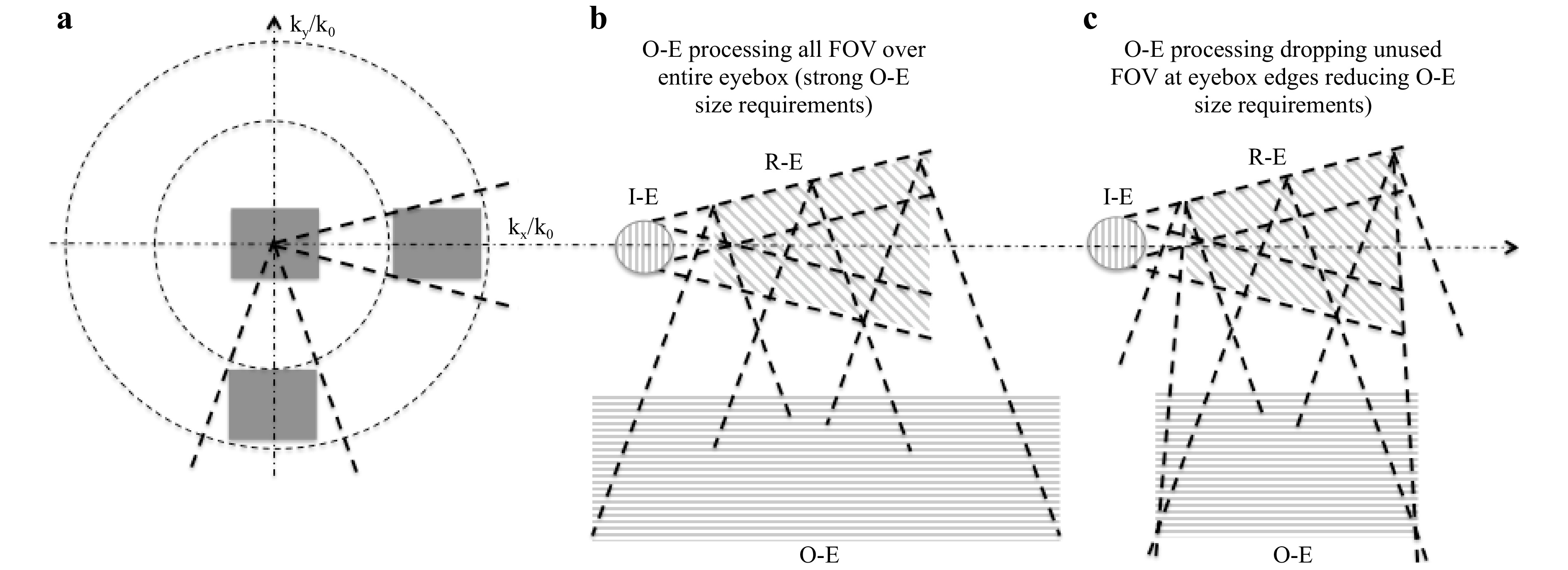
Fig. 35 Redirection and out-coupler areas as dictated by the in-coupled FOV.
The largest coupler area requirement is usually the out-coupler element (center), aiming at processing all FOVs and building up the entire eyebox. Eye relief also strongly impacts this factor. However, its size can be reduced in a “human-centric optical design” approach: the right part of the FOV at the left edge of the eyebox as well as the left part of the FOV at the right edge of the eyebox can be discarded, thus considerably reducing the size of the O-E without compromising the image over the eyebox. Note that in Fig. 34 the k-vector diagram (a) shows the FOV, whereas the lateral schematics of the waveguide in (b) and (c) show the actual size of the coupler regions.
Reducing the input pupil can help to reduce the overall size and thickness of the combiner. However, the thickness of the guide must be large enough not to allow for a second I-E interaction with the incoming pupil after the first TIR bounce. If there is a second interaction, then by the principle of time reversal, part of the light will be out-coupled and form a partial pupil (partial moon if the input pupil is circular) propagating down the guide instead of the full one. This is more pronounced for the smallest field angle, as depicted in Fig. 36.
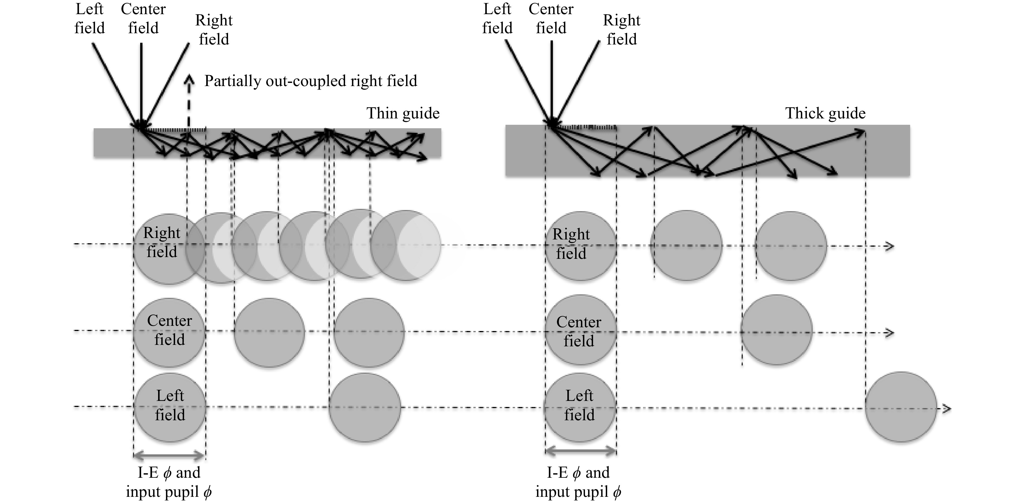
Fig. 36 Effects of the input pupil size (and size of the I-E) and thickness of guide on a single field TIR pupil bouncing down the guide.
However, if the polarization of the field is altered after the first TIR reflection at the bottom of the guide, the parasitic outcoupling can be reduced if the I-E is made to be highly polarization sensitive.
Reducing the waveguide thickness can also produce stronger pupil diversity over the eyebox and thus better eyebox uniformity. If reducing the guide is not an option (for parasitic out-coupling of the input pupil and also for etendue limitations in the display engine), a semi-transparent Fresnel surface can be used inside the guide (as in two guides bounded together), which would reflect only part of the field and leave the other part unperturbed, effectively increasing the exit pupil diversity.
Fig. 37 shows how the space of the out-coupler grating is dictated solely by the FOV and the eyebox. Note that many fields can be cancelled at the edges and towards the edges of the eyebox, as they will not enter the eye pupil (right fields on the left eyebox edge and left fields on the right eyebox edge). This can also reduce the size of the redirection grating considerably. This holds true for both eyebox dimensions.
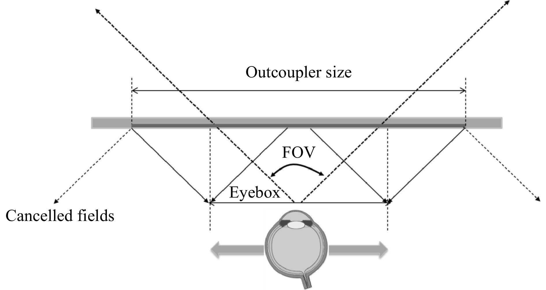
Fig. 37 Eyebox and FOV dictate the size of the out-coupler area.
-
Reducing the number of plates without altering the color of the image while propagating the maximum FOV allowed by the index of the guide is a desirable feature since it reduces the weight, size and complexity of the combiner, and make it also less prone to MTF reductions due to guide misalignments. Both lateral and longitudinal angular waveguide misalignments will contribute to a reduction of the MTF built by the display engine. Waveguide surface flatness issues are yet more cause for MTF reduction.
Due to the strong spectral spread of the in-coupler elements (gratings, holograms, RWGs, or metasurfaces), the individual color fields are coupled at higher angles as the wavelength increases, which reduces the overall RGB FOV overlap that can propagate in the guide within the TIR conditions (smallest angle dictated by the TIR condition and largest angle dictated by pupil replication requirements for a uniform eyebox). This issue is best depicted in the k-vector diagram on the right side of Fig. 38.
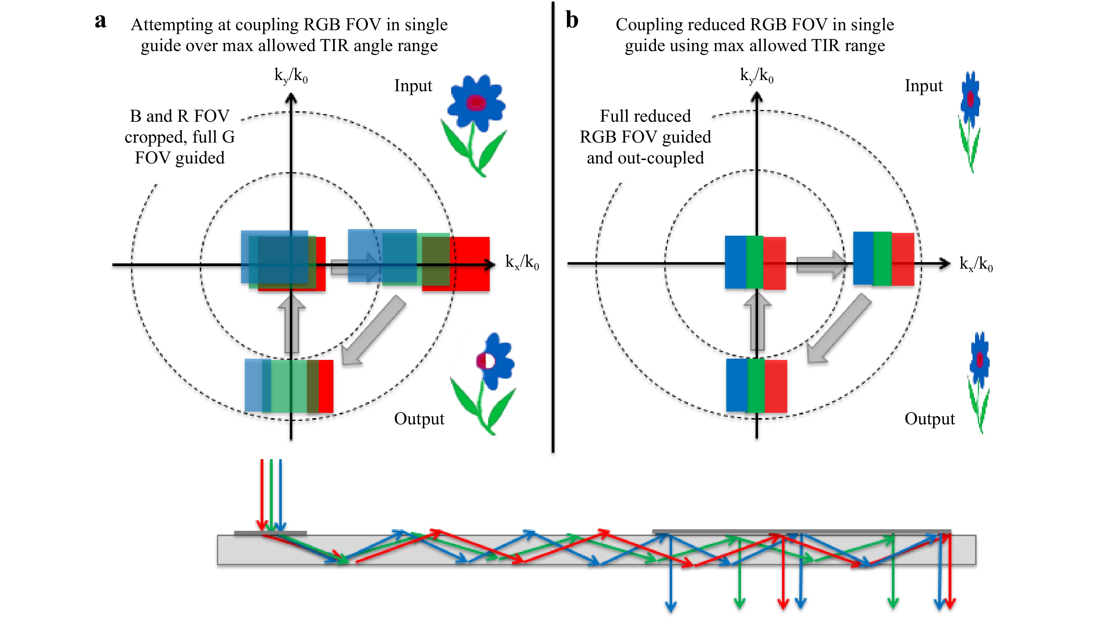
Fig. 38 k-vector diagram of a single-plate waveguide combiner using a RGB FOV coupling over a single-color TIR angular range condition and b RGB reduced FOV sharing the same TIR range.
A lower spectral spread, such as through a prism in-coupler, would increase the RGB FOV overlap in a single guide, such as in an LOE (embedded partial mirrors out-couplers) from Lumus or in the micro-prism array couplers from Optinvent.
The left configuration in Fig. 38 acts as a hybrid spatial/spectral filter, filtering the left part of the blue FOV, allowing the entire green FOV to be propagated (if the grating coupler periods have been tuned to match the green wavelength), and filtering the right part of the red FOV. The configuration in Fig. 38 propagates the entire RGB FOV (assuming the couplers can diffract uniformly over the entire spectrum) at the cost of the FOV extending in the direction of the propagation. However, when considering binocular vision, this limitation could be mitigated by engineering a symmetric color vigneting in each eye (particularly on blue and red), providing a uniform stereo color vision in a single RGB guide with high FOV (e.g., Dispelix Oy).
Recently, two plate RGB waveguide combiner architectures have been investigated, reducing by one-third the weight and size of traditional three-guide combiners, where the green FOV is shared between the top and bottom layer (see Fig. 39). Various companies are using this two-plate RGB waveguide combiner architecture today, including Vuzix, WaveOptics and Digilens.
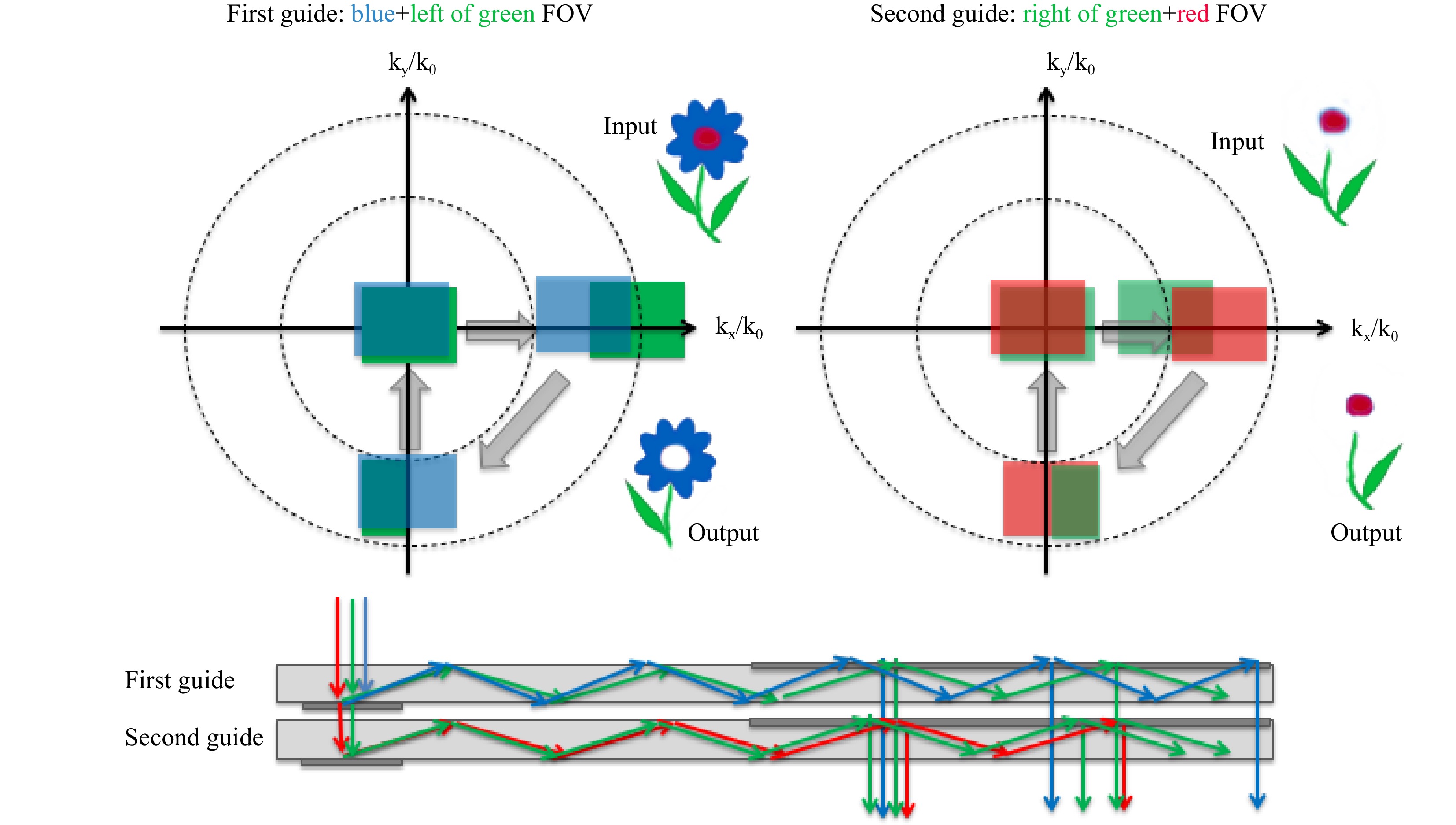
Fig. 39 Two-guide RGB waveguide combiner configuration.
However, this requires the grating (or holograms, RWGs, or metasurfaces) to be efficient over a larger spectral band, which implies that surface relief gratings are to be replicated in a higher refractive index, widening their spectral (and angular) bandwidths. High-index grating replication by NIL stretches the traditional wafer-scale NIL resin material science (inclusion of TiO2 or ZrO2 nanofiller particles). Nano-imprint at a Gen2 panel size of higher-index inorganic spin-on glass material might be the best fit, which also solves the resin or photopolymer reliability issues over various environmental conditions (temperature, pressure, shear, UV exposure, and humidity).
This two-guide RGB configuration splits the green FOV in two at the in-coupler region and merges them again over the out-coupler region. For good color uniformity over the FOV and the eyebox, especially in the green field, this technique requires perfect control of the two-guide efficiency balance. Pre-emphasis compensation of the guide mismatch is possible using the display dynamic range, but this requires precise calibration, reduces the final color depth, and does not solve the stitching region issue where the two fields overlap.
An alternative to the architecture uses the first guide to propagate green and blue FOVs and the second guide to propagate only the red FOV, as green and blue are closer spectrally to each other than red. This change, however, slightly reduces the allowed FOV traveling without vignetting but solves the green FOV stitching problem.
Although going from three plates to two plates brings a small benefit in size, weight, and cost, the added complexity of the color split geometry and the resulting color non-uniformities over the eyebox might overshadow the initial small benefits.
A single-plate RGB waveguide combiner would provide a much stronger benefit, as there is no need to align multiple guides anymore, because everything is aligned lithographically by NIL inside the single plate (potentially also front and back). This would also yield the best possible MTF and the lowest costs.
One single-plate solution is to phase multiplex three different color couplers with three different periods into a single layer, and then tune it so that there is no spectral overlap (no color ghost images over the eyebox). Such phase multiplexing is theoretically possible in volume holograms. This might be achieved in the Akonia (now Apple) thick holographic material (500 microns). If a thinner photopolymer (less than 20 microns) is desired for better reliability and easier mass production, a large holographic index swing is required. Standard photopolymers can be panchromatic and can also be phase multiplexed, but the resulting efficiency remains low, and color cross-contamination between holograms is an additional issue. This is also theoretically possible with surface relief gratings, but it is difficult to simultaneously achieve high efficiency and a high extinction ratio over the three color bands. Metasurfaces and RWGs can theoretically produce such phase-multiplexed layers but with the same limitations.
-
Smart glasses are pushing for smaller form factors and thus asking to integrate more functionality of the waveguide than simple optical combining. This is particularly true in smart glasses as the waveguide is the largest area available to the optical designer on the entire system.
Such added functionality on the same waveguide platform may come in many flavors, and a non exhaustive list is shown below:
- Optical combiner (original functionality, either in mirror or periscope modes
- Focus lens to bring the far field image at a more comfortable position to reduce Vergence Accommodation Conflict (VAC), such as in Magic Leap 1.
- Integration of prescription (Rx) lens as it is done in the Zeiss Tooz curved waveguide (low index glue separating the TIR waveguide and the Rx lens).
- Eye tracking illumination (LEDs) and eye tracking sensors (CMOS sensors)
- Head tracking sensors
- Gesture sensing
- Face tracking sensors (both optical and non optical)
- Wireless antennas (wifi, BT, 5G)
- Resolution enhancement features (optical wobulation).
Optical wobulation is an old concept which is again highly desirable especially since novel microdisplay panel technologies are being developed (microLED panels) with high brightness but still low resolution for the coming years. Optical wobulation can thus take advantage of such high brightness microdisplays are producing from a low Pixel Per Inch (PPI) a higher Pixel Per Degree (PPD) in the angular space through time domain multiplexing (see Fig. 40).
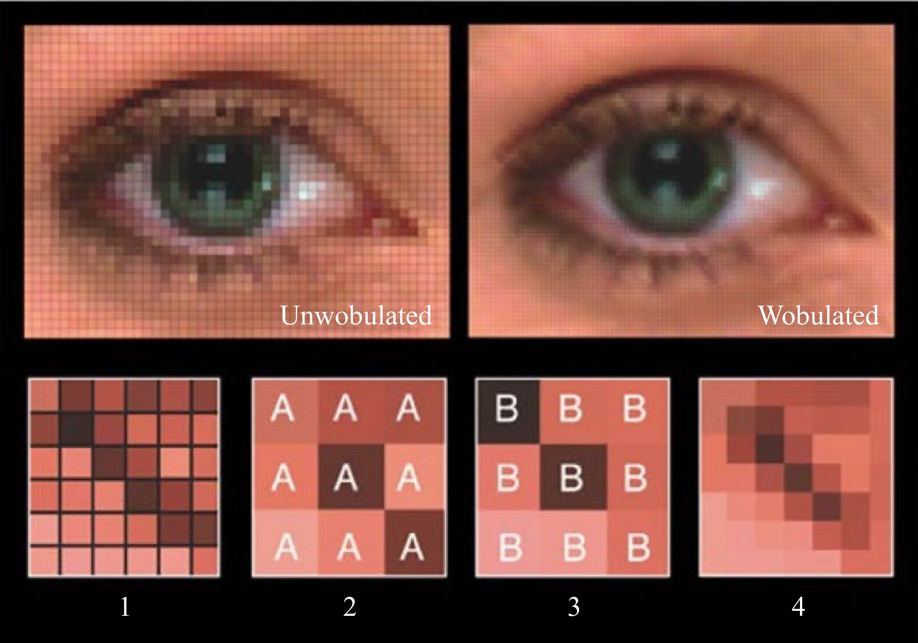
Fig. 40 Optical wobulation creating a high PPD experience from a low PPI panel.
In a smart glass form factor, optical wobulation can be done in various ways, in the illumination system of the display engine, on the display panel itself, in the pupil forming system of the display engine or directly in the waveguide combiner, as shown in Fig. 41.
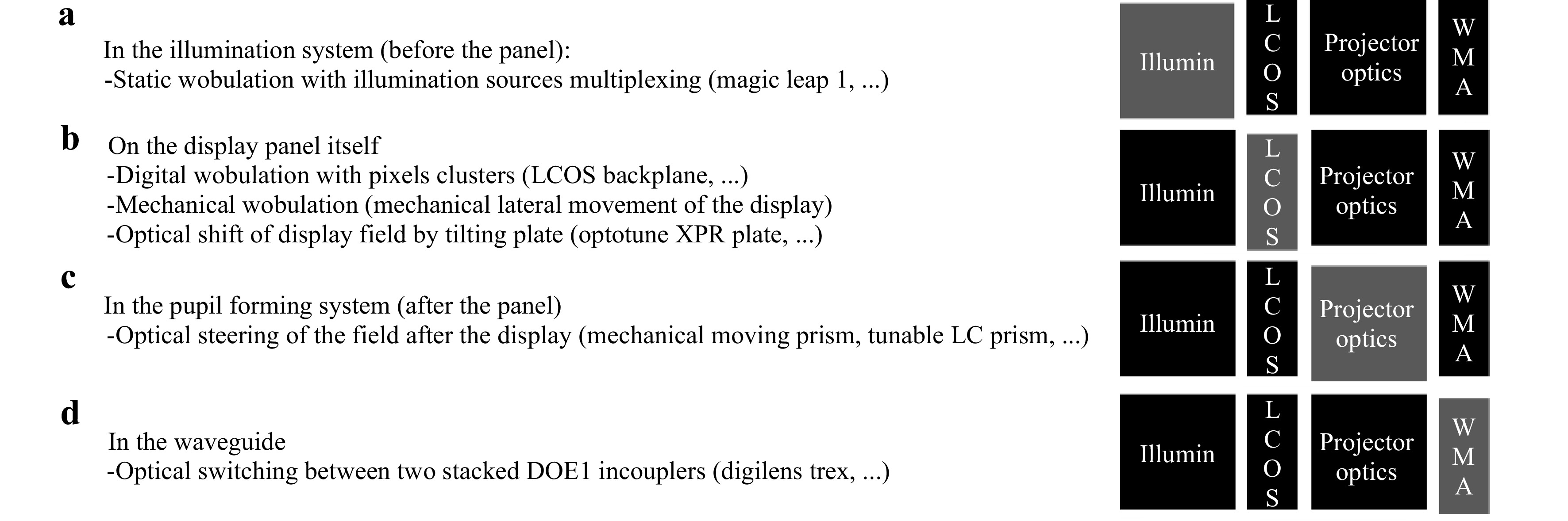
Fig. 41 Optical wobulation architectures for AR HMDs.
Today, various implementations have been investigated, from illumination system wobulation to display panel wobulation (Optotune XPR) to waveguide wobulation (Digilens Trex). They are described in Fig. 42.
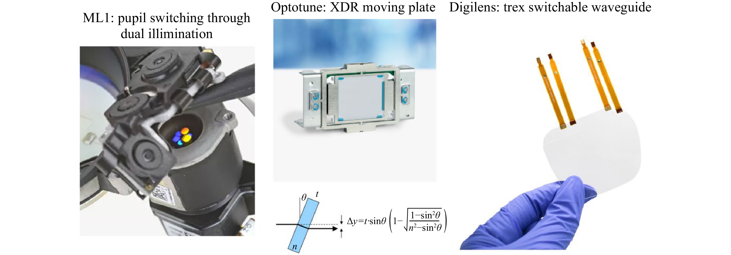
Fig. 42 Optical wobulation architectures for AR HMDs.
Although pupil switching, as done in Magic Leap 1, was not intended for optical wobulation but rather for waveguide focus switching, it could be nevertheless a good candidate assuming that various spatially demultiplexed input pupil couplers have slightly different grating periods providing a fraction of a pixel shift in the TIR field.
Optotune XPR is a moving part wobulator producing a display shift at the display panel plane.
Digilens Trex waveguide optical wobulator is providing a true optical wobulation without the need for spatially demultiplexing input pupils as with Magic Leap 1 illumination switch. Also, it does not alter the dimension of the display engine since all is done in the waveguide. It is therefore a good candidate for small form factor wobulation in smart glasses.
The cost saving by using an off the shelve smaller display panel (LCOS, DLP or microLED) is desirable especially if the wobulator does not affect the overall size of the display engine. The power savings by using a smaller panel are however compensated in part by the additional power required to drive the wobulation system (expect for illumination switch wobulation).
One step further would be to increase the angular shift to an integer number of pixels on top of a sub-pixel shift so that an optical foveation feature can be implemented, producing a foveated high PPD experience in the angular/time space with a uniform low resolution PPI display panel.
Gaze contingent optical foveation could also be implemented in such waveguide by the use of additional switchable input gratings multiplexed in various ways on the waveguide.
We will certainly see in the coming years more ways to increase the functionality of the waveguide combiner, especially for smart glasses, as it is the largest area available to the designer on the glasses to implement both display, field combining, sensing and communication functions all in a transparent medium.
-
The aim of this paper is to capture the state of the art in waveguide combiner systems for AR and MR headsets, especially as diffractive waveguide combiners (surface relief diffractives, volume holographic and others such as metasurfaces, resonant gratings etc…). We also reviewed the various reflective (or geometric) waveguides combiner architectures which can provide greater efficiency, great color uniformity and high MTF. Lately, such reflective waveguide architectures have been integrating two-dimensional pupil replication, as did previously their diffractive counterparts.
For optimal system efficiency, the lightguide, display engine and sensors need to be co-designed as a global system to match the human visual system through human-centric optical design.
The coming years will be an exciting time for AR VR MR hardware development. A full ecosystem to allow for mass production and lower costs of waveguide grating combiners is growing worldwide, including high index ultra-flat glass blanks, high index resin material developers, process equipment developers, nanoimprint lithography equipment developers, novel non-contact surface relief grating replication process, and also dedicated software design tools developers allow finally this technology to emerge as a viable option for the upcoming consumer Mixed Reality and smart glass market.
One key aspect of next waveguide developments is to include more functionality in a single waveguide, not only for field combining, but also for focus tuning, prescription lens integration, sensing and even optical wobulation and gaze contingent optical foveation.
However, one has to remember that delivering on the promises of the ultimate wearable display hardware is only one aspect of the trial and opportunity ahead for Mixed Reality, delivering on strong use cases, especially for consumer markets, will be the other critical item to consider.
Holographic optics in planar optical systems for next generation small form factor mixed reality headsets
- Light: Advanced Manufacturing 3, Article number: 42 (2022)
- Received: 06 December 2021
- Revised: 27 June 2022
- Accepted: 28 June 2022 Published online: 02 August 2022
doi: https://doi.org/10.37188/lam.2022.042
Abstract: Helmet Mounted Displays (HMDs), such as in Virtual Reality (VR), Augmented Reality (AR), Mixed reality (MR), and Smart Glasses have the potential to revolutionize the way we live our private and professional lives, as in communicating, working, teaching and learning, shopping and getting entertained. Such HMD devices have to satisfy draconian requirements in weight, size, form factor, power, compute, wireless communication and of course display, imaging and sensing performances. We review in this paper the various optical technologies and architectures that have been developed in the past 10 years to provide adequate solutions for the drastic requirements of consumer HMDs, a market that has yet to become mature in the next years, unlike the existing enterprise and defense markets that have already adopted VR and AR headsets as practical tools to improve greatly effectiveness and productivity. We focus specifically our attention on the optical combiner element, a crucial element in Optical See-Through (OST) HMDs that combines the see-through scene with a world locked digital image. As for the technological platform, we chose optical waveguide combiners, although there is also a considerable effort today dedicated to free-space combiners. Flat and thin optics as in micro-optics, holographics, diffractives, metasurfaces and other nanostructured optical elements are key building blocks to achieve the target form factor.
Rights and permissions
Open Access This article is licensed under a Creative Commons Attribution 4.0 International License, which permits use, sharing, adaptation, distribution and reproduction in any medium or format, as long as you give appropriate credit to the original author(s) and the source, provide a link to the Creative Commons license, and indicate if changes were made. The images or other third party material in this article are included in the article′s Creative Commons license, unless indicated otherwise in a credit line to the material. If material is not included in the article′s Creative Commons license and your intended use is not permitted by statutory regulation or exceeds the permitted use, you will need to obtain permission directly from the copyright holder. To view a copy of this license, visit http://creativecommons.org/licenses/by/4.0/.

 DownLoad: