


HTML
-
The field of micro-optics has been transformed by the use of femtosecond direct laser writing as a 3D printing technology since the early 2000s. Both the complexity and surface quality have advanced from simple microlenses1, 2 and achromats3 to multi-lens and multi-aperture objectives4,5. A similar development has occurred with diffractive optics, which have evolved from simple gratings6 to stacked diffractive microlens systems7. Along with imaging optics, photonic crystals8, waveguides9,10, and collimators11, complex beam shapers12-14 have been demonstrated. This rapid development reflects the significant potential of 3D printing technology in micro-optics. Advancements have enabled access to the millimetre scale and larger with 3D printing technology15-17. Meanwhile, the almost unlimited optical design freedom that it offers makes further miniaturisation possible, thereby increasing the given functionality in decreasing volumes on the micrometre scale. The aim of this study was to enhance both the complexity and miniaturisation of 3D-printed micro-optics and to create an entire integrated measurement system, a spectrometer, in a 100 × 100 × 300 µm3 volume.
The miniaturisation of spectroscopic measurement devices opens novel information channels for size-critical applications. For instance, medical engineering, consumer electronics, and downscaled chemical engineering could benefit from a cost-effective, efficient, and readily integrated spectroscopic micro-device. Spectra could be retrieved from the tip of a distal-chip endoscope with a bending radius smaller than that of an optical fibre to explore regions that are otherwise inaccessible. With the size of one or two orders of magnitude smaller than a smartphone camera objective, integration into consumer electronics is realisable for applications such as skin disease diagnosis18 and counterfeit bank note detection19. Furthermore, chemical micro-reactors (such as that proposed by Potyrailo et al.20) could be further miniaturised by precise absorption and emission line observation via 3D-printed miniature spectrometers integrated into a microreactor platform.
Various concepts for miniaturised spectrometers have been demonstrated and commercialised. There are three main categories for these spectrometers: direct, computational and filter-based. Spectrometers in the first category create a spatial-spectral response by redistributing incoming light, which can be measured directly by a line or image sensor. Spectrometers in the second category create a mixed but spectrum-dependent unique signal from which the original spectrum can be computationally reconstructed (wavelength multiplexing). The third category combines all concepts with narrowband wavelength filtering per filter patch. The 3D-printed spectrometer presented in this paper is assigned to the first class of direct spectrometers.
To the best of our knowledge, direct spectrometers presented in the literature possess a footprint area that is at least two orders of magnitude larger than our 3D-printed spectrometer (see Fig. S1). These range from commercial grating spectrometers21, 22 and scanning micro-opto-electro-mechanical system spectrometers23 to integrated approaches with digital planar holograms24 or ring-resonator enhancement25. An exceptionally high ratio of bandwidth per resolution has been reached with a grating multiplexing approach in a centimetre-size range26. Meanwhile, the footprint is reduced by two to six orders of magnitude in our 3D-printed spectrometer, whereas the spectral bandwidth per resolution ratio of these direct spectrometers can be one to three orders of magnitude higher.
In the computational spectrometer category, several new technologies have been proposed, such as colloidal quantum dot27 or photonic crystal slab28 patches for wavelength multiplexing. The single patches are in the 100-micrometre size range; however, an entire spectrometer consists of multiple patches. Thus, the filter size must be multiplied accordingly. It is our understanding that only two spectrometers have been demonstrated in which the system sizes are of the same order of magnitude as our footprint of 100 × 100 µm2. They are based on nanowires29, 30 or disordered photonic structures31, and they have a bandwidth per resolution ratio that is similar to the one in our approach. However, owing to wavelength multiplexing, the system must be calibrated with an iterative reconstruction algorithm to deduce the original spectrum. In contrast, we present an angularly insensitive spectrometer with a directly separated spatial-spectral response.
The third category, filter, based spectrometers-is based on traditional concepts, such as dyes or Fabry-Pérot etalons, along with recent concepts, such as nanowire grids, plasmonic nanohole arrays, quantum dots32, colloidal quantum dot sensors combined with Bragg mirror filter arrays33, and ultrafast pyroelectric metasurfaces34. However, owing to their narrow bandwidth filtering, a considerable portion of the signal is lost. In contrast, our 3D-printed spectrometer collects light with a numerical aperture (NA) that is larger than 0.4, a light collection area of 50 × 50 µm2 at the first lens, and redistributes the wavelengths with minimal losses.
Overall, the 3D-printed miniature spectrometer presented herein marks an innovation for 3D-printed micro-optics in terms of complexity, while exploiting for the first time the micrometre size range for direct spectrometers.
-
We assessed the performance of the spectrometer in a miniature volume of 100 × 100 × 300 µm3 for a wavelength range of 490 nm to 690 nm. In the design concept (Fig. 1a), the strengths of 3D printing are considered: freeform surfaces and inherent near-perfect alignment owing to simultaneous mount and lens fabrication, which enable heavily tilted and asymmetrical surfaces. Incoming light is collected by a cylindrical lens with a quadratic aperture of 50 × 50 µm2, which corresponds to an NA of 0.42 in the
$ y $ -direction at the slit. The slit is realised not in air but in a photopolymer to serve simultaneously as an ink barrier. The diverging rays exiting the slit are collimated by the subsequent surface. This collimation lens is terminated by a tilted surface to compensate for the grating deflection angle in advance, thereby keeping the spectrometer within its narrow footprint. The grating surface is then illuminated by the collimated rays. The last surface serves as an imaging lens to separate the wavelengths at an output plane nearby, such as for an image sensor in future applications. The full spectrometer thus has a length below 300 µm, which is inside the high-precision piezo z-stage range of the 3D printer. This last surface is also tilted with respect to the grating surface and thus restricts the chief ray angles (CRAs) at the output image plane to a maximum angle of 16° at 690 nm wavelength. Therefore, each field could be coupled efficiently without crosstalk into an image sensor pixel with CRA limitations.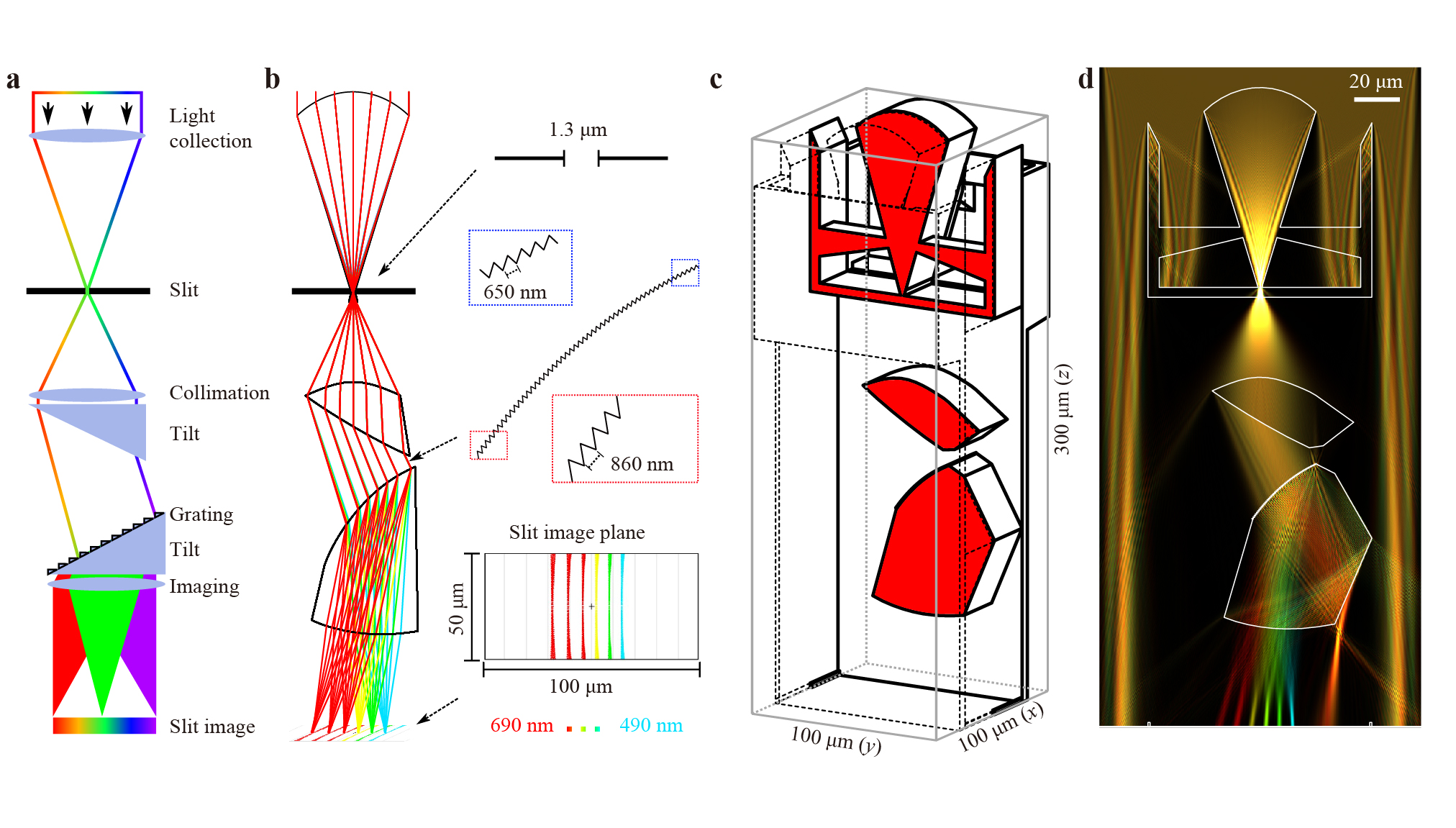
Fig. 1 Optical design and simulation of the miniature spectrometer.
a Design principle. b Optical design and ray-tracing simulation. Slit width, blazed grating, topography, and footprint spot diagram are highlighted for the indicated surfaces. c Cut view of the 3D-printed volume model. Lenses, grating, slit, and mounts are printed in one step and fit in a volume of only 100 × 100 × 300 µm3. d Two-dimensional wave-optical simulation (WPM) of the plane highlighted in red in c. Around the slit a perfectly absorbing material is assumed. Simulation wavelengths are in the visible range from 490 nm to 690 nm in 40 nm steps.The implementation of the described design principle is shown as a sequential ray-tracing model in Fig. 1b. In extending the general design concept, slight curvatures and aspherical extensions were permitted for the tilt and grating surfaces to minimise aberrations. Detailed surface type descriptions are given in the Materials and Methods section. The most important functional surfaces of the spectrometer are highlighted on the right side of the figure. Because the spectrometer size is in the micrometre range, diffraction must be considered for the slit design. The slit width was designed to be 1.3 µm to create a single slit diffraction pattern with an opening angle that is suitable for the collection NA of 0.42 (with regard to its first minima positions at 550 nm).
The grating is designed to consist of as many lines as can be manufactured to maximise the spectrometer resolution. The fabrication process generally accommodates feature sizes down to 100 nm35. However, if the photoresist is printed as a bulk material, as in the case of the grating, the resolution decreases owing to the accumulated laser energy, and thus polymerisation increases in the laser focus vicinity. Consequently, the grating period was restricted to a minimum period of 650 nm to be sufficiently resolved (see Fig. S3).
The first diffraction order of the grating is used as the spectrometer measurement signal. The grating topography was thus established for maximum diffraction into the first diffraction order. Both the zeroth and second order are spatially separated such that the measurement signal is not affected. The period is chirped and spans from 650 nm to 860 nm across the grating width of 38 µm. This is a considerably smaller portion of the 100 µm footprint for two reasons. First, the total length of the spectrometer is restricted to < 300 µm. Therefore, the beam paths for collecting, expanding, and collimating the light were constrained. Second, the width of the collecting lens is limited to 50 µm; hence, a 25 µm circumferential gap enables the needle to access and apply the super-fine inkjet process described later in this section. The combination of these two restrictions leads to the beam width of 38 µm at the grating surface. Ultimately, the median frequency is 1.34 μm−1 and
$ N= $ 51 grating lines are illuminated. This results in a theoretical resolution limit of Δλ = λ/N = 10.4 nm at$ \mathrm{\lambda }=532 $ nm and$ \Delta \mathrm{\lambda }= $ 12.4 nm at$ \mathrm{\lambda }=633 $ nm for diffraction-limited performance.In the ray-tracing simulation, all fields were emitted from a point in the centre of the slit at
$ x=y=0 $ . Because the lenses have a cylinder-like shape, the$ x $ -direction is not focused. The slight curvature of each dispersed slit image in the footprint spot diagram is ascribed to conical diffraction as a result of tilted rays at the grating surface in the$ x $ -direction.The lenses were integrated into a printable computer aided design (CAD) model, including an ink basin (Fig. 1c). The central
$ yz $ plane at$ x=0 $ (indicated in red) was investigated wave-optically using the wave propagation method36, 37 (WPM) for plane-wave illumination (Fig. 1d). The terminating lens surfaces, e.g. the right edges of the lowest lens block, were designed such that the WPM simulation resulted in a sufficient separation of the zeroth diffraction order from the first order of interest without exceeding the footprint. Accordingly, multiple spectrometers could be printed in close vicinity without crosstalk. The first-order diffraction is visible as being coloured with separated foci, while the non-dispersed zeroth order is initially reflected at the right lens edge and redirected to the right part of the slit image plane, which is well separated from the first-order foci.Furthermore, the focal length of the last lens was optimised such that the first diffraction order is focused within the working distance of the printing objective in the
$ z $ -direction (< 300 µm total length of the spectrometer), which is also within the high-precision piezo z-stage range of the 3D printer. This restriction enables repeated closely spaced printing of the spectrometers directly onto the sensor surface with consideration of the fabrication modalities.In the next step, the spectrometer was fabricated via two-photon direct laser writing (DLW). Subsequently, the absorbing structure around the slit was realised by the application of a super-fine inkjet process38, 39 (details are given in the Materials and Methods section). The inkjet process and final miniature spectrometer are shown in Fig. 2a. Both the two-photon DLW and the inkjet process were repeatedly applied; thus, an array could be fabricated, as shown in the figure.
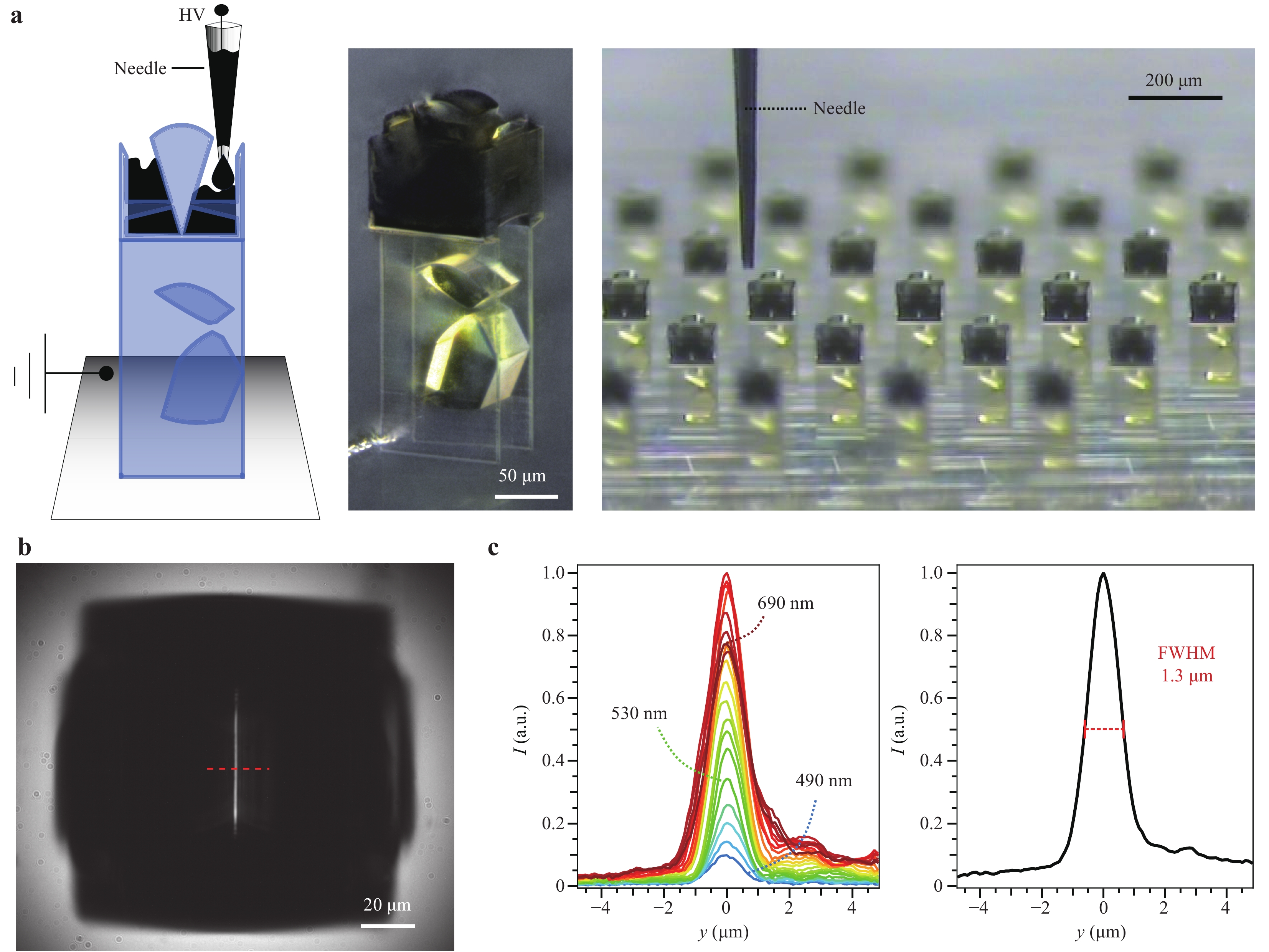
Fig. 2 Slit fabrication and measurement.
a Super-fine inkjet printing principle, complete fabricated spectrometer with 100 × 100 × 300 µm3 volume, and slit fabrication of a microspectrometer array. b Transmission image of the slit at 530 nm illumination wavelength. The profile position is indicated as a dashed red line. c Profiles of the slit image for wavelengths from 490 nm to 690 nm in 10 nm steps and average of the normalised profiles.To quantify the spatial filtering of the slit, only the upper part of the spectrometer was fabricated. For this purpose, the CAD model was cut between the bottom of the ink basin and the collimation lens. The collector lens was illuminated with wavelengths ranging from 490 nm to 690 nm, and the slit was measured with a monochromatic video microscope (Fig. 2b). From the microscope image, an intensity profile was obtained as indicated. The profiles for each wavelength and all normalised and subsequently added profiles are shown in Fig. 2c. The spectral distribution of the profiles reflects the absorption of the photoresist IP-Dip40 combined with the spectral distribution of the monochromator that was used for the measurement (see Fig. S2). The average slit width at full width half maximum (FWHM) is 1.3 µm, which is in good agreement with the design. To quantify the signal-to-noise ratio, a sinc2 function with a FWHM of 1.3 µm is subtracted from the measurement data, and the remaining positive signal is regarded as noise. The maximum noise level is 15%, while the average noise level is 5% ± 3%.
The miniature spectrometer was experimentally characterised using the setup depicted in Fig. 3. A fibre-coupled monochromator or laser (only for the linewidth measurement) is used as illumination source. The output facet of the fiber is imaged with a 100x microscope objective (focal length
$ f=2 $ mm) to the front of the 3D-printed spectrometer. This configuration is used for multiple reasons. First, the illumination is concentrated on the region of interest, namely the spectrometer. Second, stray light from outside the 100 × 100 µm2 footprint is suppressed. In a real-world application, stray light could be shielded by a chromium aperture without tight alignment tolerances at the spectrometer front. Third, the angular extent of the fibre facet emission is increased owing to the magnification of −0.13 and the high NA of 0.9 of the described imaging setup. Accordingly, the angular insensitivity of the spectrometer, that is, the successful spatial filtering, can be demonstrated.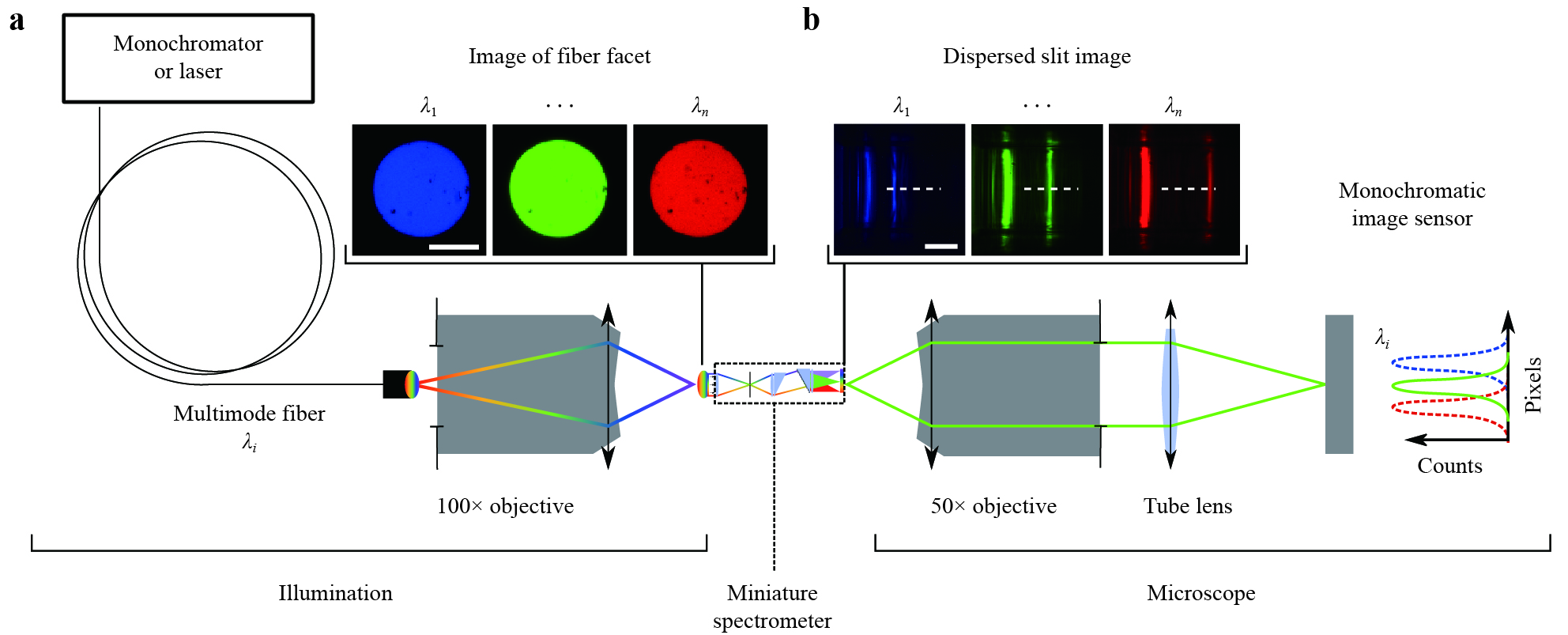
Fig. 3 Measurement setup.
a Illumination side: A fibre-coupled monochromator or laser is imaged to the front of the miniature spectrometer. b Microscope side: The image plane of the spectrometer is magnified with a microscope. The dispersed image of the slit (first diffraction order, right) shifts corresponding to the illumination wavelength while the zeroth diffraction order (left) is stationary and spatially separated from the region of interest. The profile position for further evaluations is indicated as a white dashed line. The monochromatic measurements of the fibre facet and slit images are coloured for visualisation. Scale bars 20 µm.On the microscope side of the measurement setup (Fig. 3b), the dispersed slit image plane is recorded with a 50x microscope objective with an NA of 0.55 combined with a tube lens and a monochromatic image sensor. In the recorded images, the first diffraction order is visible as a tight line that moves in the
$ y $ -direction when shifting the wavelength. In contrast, the zeroth order is stationary at the left end of the recorded images. To measure the spatial-spectral response, an intensity profile across the centre of the first-order movement range is recorded, as indicated by the white dashed line.In Fig. 4a, the normalised spatial-spectral response measured at the slit image plane of the spectrometer is shown for a wavelength range from 490 nm to 690 nm in 10 nm steps. The peaks of the single profiles are well separated, and the medium noise level is on the order of 5% to 20%. Each profile can be fitted with a sinc2 function to eliminate the noise, as depicted in Fig. 4b. The width of the single wavelength profiles underestimates the resolution capacity of the miniature spectrometer because the monochromator-line spectral width has a similar magnitude as the resolution capacity to be measured. Fig. 4e depicts the resolution capacity.
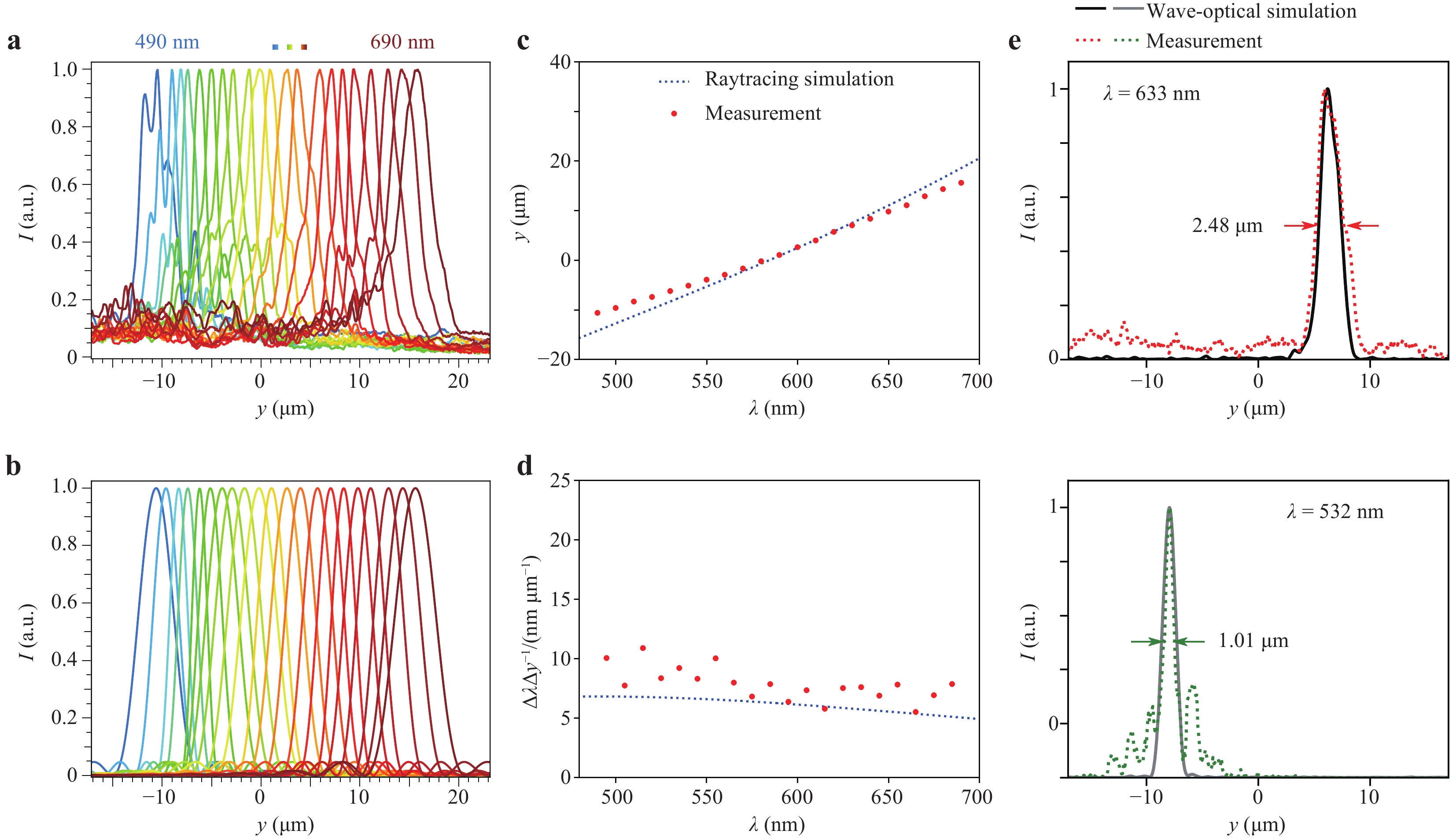
Fig. 4 Spatial-spectral response of the miniature spectrometer.
a Measured normalised intensity profiles at the image plane of the spectrometer for illumination wavelengths ranging from 490 nm to 690 nm in 10 nm steps (monochromator, profile position is indicated in Fig. 3b). b Sinc2 fits of the intensity profiles from a. c Centre positions of the sinc2 fits per wavelength. d Wavelength shift per micrometre deduced from c. e Linewidth simulation and measurement with a red or green laser, respectively. The measured full width at half maximum is indicated with a pair of arrows. The combination of measurements d and e yield a spectral resolution of 9.2 ± 1.1 nm at 532 nm and 17.8 ± 1.7 nm at 633 nm wavelength.The wavelength-dependent centre positions of the sinc2 fits are plotted as
$ y $ -positions or wavelength shifts per micrometre, respectively, in Fig. 4c and d. These fitted measurement data are consistent with the respective ray-tracing simulation data; however, the wavelength shift per micrometre is larger in the measurement than in the simulation. This is presumably due to the shrinkage of the photoresist, which leads to a focus shift towards the last lens block and thus to closer spacing of the wavelengths.The spectral resolution of the miniature spectrometer was assessed with narrow bandwidth illumination sources (green laser at
$ \lambda = 532 $ nm and helium neon laser at$ \lambda = 633 $ nm) (Fig. 4e). These two laser wavelengths sample the resolution in the shorter wavelength range ($ 532 $ nm) and the longer wavelength range ($ 633 $ nm) of the total spectral range of our spectrometer. For speckle reduction, a vibrating diffuser was integrated before coupling into the multimode fibre, and multiple measurements were obtained for temporal averaging. At 532 nm illumination wavelength, the measured profile has a centre peak with a comparable and even slightly narrower FWHM linewidth than the profile simulated with the WPM. In exchange, the side lobes are more pronounced. This behaviour may be due the non-uniform illumination of the slit or grating, comparable to the intensity distribution of a Bessel function as the diffraction pattern of a ring pupil. In such a case, the FWHM width is smaller than that of the corresponding airy disc, while the side lobes carry more energy41. The resolution at 532 nm is determined from the FWHM of 1.01 µm indicated in the graph.From Fig. 4d, the measurement data of the wavelength range from 500 nm to 560 nm are averaged to calculate the medium wavelength shift per micrometre around the laser wavelength of 532 nm. Multiplication of this value by the FWHM yields a spectral resolution of 9.2 ± 1.1 nm, which is close to the diffraction limit of 10.4 nm and the wave-optical linewidth simulation of 12.5 ± 1.5 nm. The linewidth measurement at the 633 nm wavelength is evaluated accordingly. Here, the medium wavelength shift per micrometre in the range from 600 nm to 660 nm is considered. It yields a spectral resolution of 17.8 ± 1.7 nm at a wavelength of 633 nm. The wave-optical linewidth simulation suggests a slightly better resolution of 14.5 ± 1.4 nm. This deviation could be due to imperfections in the refractive optical surfaces printed with the high-resolution photoresist IP-Dip, which has some deficiencies in terms of smoothness.
Finally, the spectrum of an unknown light source (broadband multiple LED light) was recorded and compared to that of a commercial spectrometer (see Fig. 5). Because of the relatively high noise level, an averaged, weighted noise signal was subtracted from all the measured spectra (see the Materials and Methods section and Supplementary Material for further information). A wavelength-dependent calibration factor was determined by the quotient of a known spectrum (halogen lamp) that was measured with both our spectrometer and a commercial spectrometer. The measurement of the unknown light source was multiplied by this calibration factor. The unknown spectrum measurement shows a slightly lower signal in the range of 500-570 nm and a slightly higher signal in the range of 620-670 nm, with overall satisfactory accordance, although it has a footprint eight orders of magnitude smaller. Especially in the lower wavelength range, small features at distinct wavelengths that are visible on the spectrum recorded using the commercial spectrometer, are distinctly perceptible in the measurement obtained using our spectrometer.
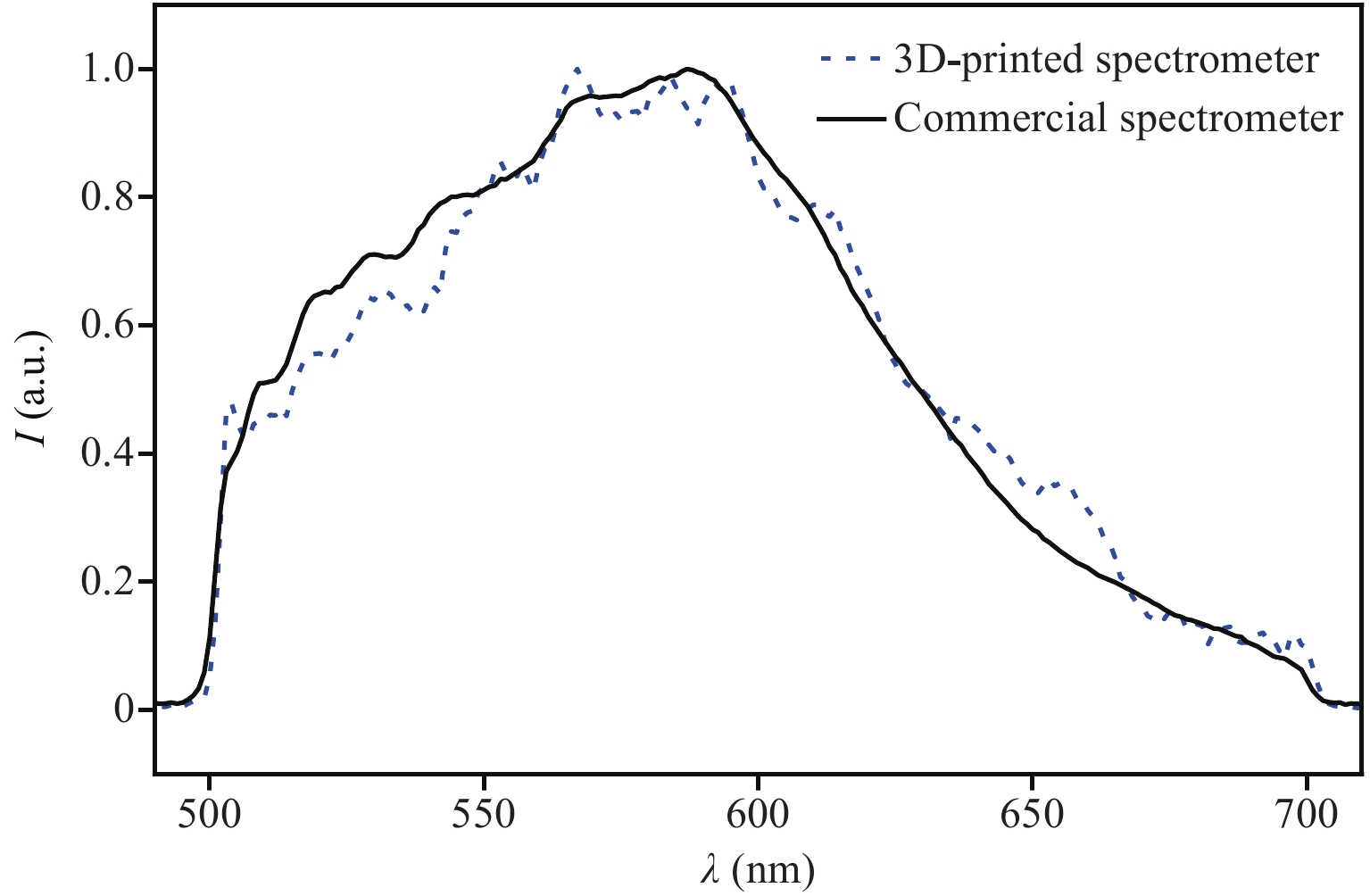
Fig. 5 Comparison of a spectrum measured with the 3D-printed spectrometer and with a commercial spectrometer.


-
The study presented herein proves the feasibility of a fully functional spectrometer fitted in a volume of only 100 × 100 × 300 µm3. The size comparison with a standard smartphone camera lens Fig. 6 highlights the potential of this technology. At a size of more than one order of magnitude smaller than the objective, the spectrometer can be integrated almost non-invasively into a smartphone camera, i.e. printed directly onto the camera sensor, such as for single spectral measurements or as individual pixels of a snapshot hyperspectral camera.
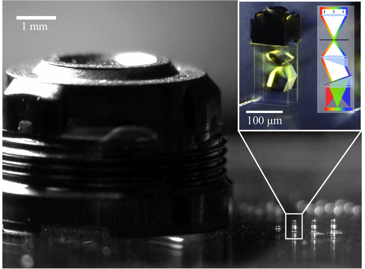
Fig. 6 Size comparison of the 3D-printed spectrometer (white box) with an iPhone 5s camera lens.
The inset shows a microscope image of the fabricated spectrometer (left) and its optical design principle (right).The feasibility of two-photon 3D printing directly onto image sensors has been demonstrated in previous studies4,5. It should be noted that the wavelength shift per micrometre has a value of 9.1 ± 1.1 nm/μm at 532 nm and 7.2 ± 0.7 nm/μm at 633 nm. Therefore, a monochromatic image sensor with a pixel pitch below 1 µm must be used to resolve the spectral lines. Current trends in this direction are evident. For example, Samsung has announced a 47.3 MP sensor with a 0.7 µm pixel pitch (ISOCELL Slim GH1). Moreover, high-resolution monochromatic image sensors have entered the mass market through Huawei Mate 9 smartphone.
Furthermore, the implementation of a spectrometer fabricated strictly by 3D printing can be highlighted as a novelty. The measured ratio of bandwidth per resolution of
$ {1}/{2}\cdot 200 \; \rm{nm}\cdot \left({1}/{\Delta {\mathrm{\lambda }}_{532}}+{1}/{\Delta {\mathrm{\lambda }}_{633}}\right)=16.5$ is in a margin similar to those of other spectrometers that have been demonstrated in this size range29, 31. In the category of direct spectrometers, the microspectrometer presented here is the first of its kind in this size range (see Fig. S1).Nevertheless, our spectrometer has a limitation in that a relatively high noise level can be identified. A possible solution could be the design of an ink basin with improved suppression enabled by an increase in the ink layer that is close to the slit. However, a slit elongated in the
$ z $ direction for improved absorptive ink layer thickness would likely decrease the spectrometer light efficiency. Another part of the noise could originate in the utilisation of the high-resolution photoresist IP-Dip, which enables small voxel sizes and is thus well suited for the creation of high-frequency grating structures. However, a deficiency of this material is the roughness of the fabricated surfaces. Kirchner et al.42 reported the surface roughness of IP-Dip on the order of 100 nm, which makes this photoresist type disadvantageous for refractive lenses. Since diffractive and refractive structures are both part of the spectrometer, the refractive surfaces are compromised. The use of a smoother photoresist, for example, IP-S, which can exhibit an optical-quality root mean square surface roughness that is below 10 nm14, could be examined in future work. This photoresist may be beneficial for spectrometers with a larger footprint and lower grating frequencies. Multi-material printing, as demonstrated by Schmid et al.3 and Mayer et al.43, could resolve these conflicting requirements. Further optimisation of 3D-printing parameters, as proposed by Chidambaram et al.44, could lead to smoother surfaces at the expense of printing time. The printing parameters have thus far been optimised with a focus on the slit and grating, which both require high resolution instead of smoothness.As presented in the introduction, our spectrometer is classified in the direct spectrometer category because of its direct spatial-spectral response. However, in combination with a computational approach, the (static) noise can be interpreted as a multiplexed wavelength signal. An iterative reconstruction algorithm, such as that used by Bao et al.27, could be employed to sharpen the spectral lines of our spectrometer. In its current configuration, the spectrometer can readily be used as a wavemeter because the centres of the sinc2 fits yield distinct results in the presence of noise. As a miniature wavemeter, it could be employed as a highly integratable laser wavelength stabiliser.
Additionally, the wavelength range of the spectrometer presented here is extendable. 3D printing comes with a high degree of individuality at a comparably low cost. Therefore, an array of slightly different spectrometers could be fabricated, with each being optimised for another part of the spectrum. This is a major advantage with regard to spectrometers fabricated using non-classical approaches, such as colloidal quantum dots27, photonic crystal slabs28, nanowires29, and disordered photonic structures31. These methods have either a rather small bandwidth or cannot be intrinsically extended to the infrared region. In our classical grating spectrometer approach, the only limit for wavelengths in the infrared region is either the transmittance of the photoresist or the absorption of the sensor that is used to record the signal. The photoresist IP-Dip has an extinction coefficient well below 0.1 mm−1 in the infrared region up to 1600 nm wavelength40. Thus, our approach could readily be employed in this region. Moreover, the design can be based on the same principle, as presented in Fig. 1. By leveraging minor adaptions of surface tilts, the grating phase profile, and re-optimisation of the aspherical surface coefficients, the spectral cut-out could be shifted towards longer wavelengths. For instance, a grid of four individual spectrometers could enable a spectrometer with a wavelength range of 800 nm on a footprint of 200 × 200 µm2.


-
In this study, the feasibility of a 3D-printed spectrometer in a miniature volume of 100 × 100 × 300 µm3 was theoretically assessed and experimentally proven. The fabricated spectrometer has a wavelength range of 200 nm in the visible range, and a spectral resolution of 9.2 ± 1.1 nm at 532 nm and 17.8 ± 1.7 nm at 633 nm wavelength. To the best of the authors' knowledge, the presented spectrometer is the first spectrometer with a direct spatial-spectral response that has been demonstrated in this size range. Compared to computational and filter-based approaches, its angular insensitivity and relatively large aperture of 50 × 50 µm2 are emphasised. A hybrid direct computational approach could significantly improve the average noise level of 5% to 20%. Wavelength range extensions of 200 nm per 100 × 100 µm2 footprint were proposed in a multi-aperture approach by implementing the same design principle for adjacent parts of the spectrum. Possible applications range from endoscopy devices and consumer electronics to chemical microreactors.
-
The proposed spectrometer was designed using ZEMAX OpticStudio optical design software in the sequential mode for a wavelength range of 490 nm to 690 nm. The glass model that was utilised is the photoresist IP-Dip presented by Gissibl et al.45. For ray tracing, the spectrometer was divided into two parts: the light collector (part 1, top lens to slit) and the dispersing imager (part 2, slit to the dispersed slit image plane). All surfaces except the grating surface and the photoresist/air interface behind the slit are described by a toroidal surface with a rotation radius of infinity. The surfaces have a cylinder-like shape with a 50 µm extension in the
$ x $ -direction. The surface sags$ {z}_{toroidal}\left(y\right) $ are defined by$$ {z}_{toroidal}\left(y\right)\!=\!\frac{c{y}^{2}}{1\!+\!\sqrt{1\!-\!{c}^{2}{y}^{2}}}\!+\!{a}_{1}{y}^{2}\!+\!{a}_{2}{y}^{4}\!+\!{a}_{3}{y}^{6}\!+\!{a}_{4}{y}^{8}\!+\!{a}_{5}{y}^{10} $$ (1) where curvature
$ c $ and coefficients$ {a}_{i} $ are optimisation variables. Part 1 consists of a toroidal surface with coefficients up to the second order followed by a propagation distance of 90 µm inside the photoresist to the slit. In part 2, ray-tracing for all fields starts at the centre of the slit with the same NA as the rays focused by the collector. Accordingly, spatial filtering at the slit is considered, and part 2 can be optimised for the best imaging (minimum spot width per wavelength at$ x=0 $ ) of the slit plane. After a distance of 4.5 µm, the photoresist/air interface is simulated by a plane to complete the ink basin described later in this section.The following optical surfaces, except the grating surface, are described by Eq. 1 with coefficients up to the tenth order. The grating surface is described by the sequential surface-type elliptical grating 1, and the surface sags
$ {z}_{grating}\left(y\right) $ are given by$$ {z}_{grating}\left(y\right)=\frac{c{b}^{2}{y}^{2}}{1+\sqrt{1-{b}^{2}{y}^{2}}}+{a}_{1}y+{a}_{2}{y}^{2}+{a}_{3}{y}^{3}+{a}_{4}{y}^{4}+{a}_{5}{y}^{5} $$ (2) where
$ b, \, c $ , and coefficients$ {a}_{i} $ are optimisation variables. This polynomial surface is superimposed by a phase profile resembling the variable grating period with the effective grating period$ {d}_{eff} $ defined as$$ {d}_{eff}\left(y\right)=\frac{1}{{T}_{0}}+\mathrm{\alpha }y+\mathrm{\beta }{y}^{2}+\mathrm{\gamma }{y}^{3}+\mathrm{\delta }{y}^{4} $$ (3) where the optimisation variables are
$ {T}_{0},\;\mathrm{\alpha },\;\mathrm{\beta },\;\mathrm{\gamma } $ , and$ \mathrm{\delta } $ . This phase profile was translated into a topography using MATLAB by applying the first-order blazed condition for a wavelength of 550 nm at a fixed incident angle of the chief ray to the field-dependent (chirped) grating deflection angle.Subsequent to the optical design, lens mounts and an ink basin were added to the optimised lens surfaces in the SolidWorks CAD programme. A two-dimensional scalar wave-optical simulation using the wave propagation method36, 37 (WPM) was performed with discretisation of the volume model with
$ dy=dz=20 $ nm at$ x=0 $ for a plane wave normal input that covers the full width of the spectrometer. To approximate the absorbing behaviour of the ink basin, a perfectly absorbing ($ E=0 $ ) layer was introduced to the model at the inside edges of the basin. For the results presented in Fig. 1d, a spectrum simulation of 490 nm to 690 nm in steps of 40 nm was performed. Each resulting intensity distribution was normalised to its own maximum value in the observation plane and converted to an RGB representation according to Bruton46 for display purposes.In the next step, the CAD model was sliced at a distance of 100 nm, hatched strictly in the direction of the grating lines (
$ y $ -direction) at a distance of 250 nm, and fabricated by means of 3D dip-in two-photon DLW using Photonic Professional GT2 (Nanoscribe GmbH, Karlsruhe, Germany) and the proprietary negative-tone photoresist IP-Dip44 on a glass substrate with an ITO coating. The laser source of the 3D printer is a pulsed femtosecond fibre laser with a centre wavelength of 780 nm, a specified average laser power output of 120 mW, a pulse length of approximately 100 fs at the source, and an approximate repetition rate of 80 MHz. The spectrometer was printed with 7.5 mW laser power and a scan speed of 15 mm/s. The total printing time of the single spectrometer was just below 2 h. The dispersed slit image plane coincided with the glass surface. The polymerised samples were developed in propylene glycol methyl ether acetate for 8 min to wash out the unexposed photoresist. Subsequently, the sample was rinsed in an isopropanol bath for 2 min and dried with a nitrogen blower.The slit was fabricated with the SIJ-S030 super-fine inkjet printer (SIJ Technology, Inc., Tsukuba, Japan). The ink utilised for the creation of the non-transparent structures was NPS-J (Nanopaste Series, Harimatec, Inc., Georgia, USA). It is a conductive ink that comprises a silver nanoparticle content of 65 mass % with a particle size of 12 nm. When high voltage is applied, the printer can dispense droplet volumes of 0.1 fl to 10 pl from a needle tip with a diameter below 10 µm, which fits into the gap between the collector lens and the ink basin walls. (Details on this fabrication method are provided in Toulouse et al.38, 39.) This process was applied to fill the ink basin that was defined in the CAD design.
The spatial-spectral response measurements were performed with a fibre-coupled home-built monochromator using the spectrum of a dimmable 150 W quartz halogen lamp (model I-150, CUDA Products Corp., Fiberoptic Lightsource, Florida, USA), which was used as the illumination source. The linewidth measurements were performed with a green laser source (532 nm, 5 mW) or red helium neon laser (632.8 nm, 5 mW, model 05-LLP-831, Melles Griot, Darmstadt, Germany), respectively, in combination with a vibrating diffuser coupled into the same fibre as the monochromator (300 µm, NA 0.39, model M69L02, Thorlabs, New Jersey, USA). The output fibre facet was imaged with a 100x objective with NA 0.9 (M Plan Apo HR 100X, Mitutoyo, Kawasaki, Japan) to the front of the 3D-printed spectrometer. The dispersed slit image plane of the spectrometer was recorded with a monochromatic video microscope.
The video microscope consisted of a 50x objective with NA 0.55 (50X Mitutoyo Plan Apo, Edmund Optics, New Jersey, USA) in combination with a
$ f=200 $ mm tube lens (MT-4, Edmund Optics, New Jersey, USA) and a monochromatic camera (UI-3180CP-M-GL R2, IDS, Obersulm, Germany). For the linewidth measurement, the video microscope was focused on the minimum detectable linewidth per wavelength, and the simulated linewidth was offset in the$ y $ -direction for the best fit. Before each measurement and for each wavelength, the camera integration time was adjusted to record a high signal without saturation. For each measurement, 20 images and 20 profiles in the$ x $ -direction per image were recorded and averaged after subtraction of a dark image. The slit width measurement was similarly performed; however, instead of the entire spectrometer, only part 1 (collector lens, slit, and ink basin) was fabricated and the video microscope was focused on the slit. Here, the integration time of the camera was adjusted to the overall maximum signal and was the same for all wavelengths.For all spectrum measurements, the noise was evaluated and subtracted (see Supplementary Material for further information). The wavelengths outside the spectrum of our spectrometer were filtered with a long-pass filter (pass > 500 nm) and a short-pass filter (pass < 700 nm) (models FEL0500 and FES0700, Thorlabs, New Jersey, USA). The setup shown in Fig. 3 was used. The measured profile
$ {I}_{m}\left(y\right) $ was translated into a wavelength-dependent signal$ {I}_{m}\left(\mathrm{\lambda }\right) $ by evaluating the centres of the sinc2 fits (see Fig. 4b-e). The relative intensity calibration of the spectrometer was conducted with a 150 W quartz halogen lamp (model I-150, CUDA Products Corp., Fiberoptic Lightsource, Florida, USA). A reference spectrum$ {I}_{th,halogen}\left(\mathrm{\lambda }\right) $ was recorded with a commercial spectrometer (AvaSpec-ULS2048CL-EVO-FCPC, Avantes, Mountain Photonics GmbH, Landberg am Lech, Germany) and was normalised to its maximum intensity. The calibration factor was calculated as$ k\left(\mathrm{\lambda }\right)={I}_{th,halogen}\left(\mathrm{\lambda }\right)/{I}_{m,halogen}\left(\mathrm{\lambda }\right) $ .As a light source for the unknown spectrum measurement, a white light LED (model MCWHLP1 and collimator SM2F32-A, Thorlabs, New Jersey, USA) was coupled into the multimode fibre of the measurement setup. The final spectrum measurement was calibrated as
$ {I}_{m,LED,calib}\left(\mathrm{\lambda }\right)= k\left(\mathrm{\lambda }\right)\cdot {I}_{m,LED}\left(\mathrm{\lambda }\right) $ .


-
This work was funded by Bundesministerium für Bildung und Forschung (Printoptics, Printfunction), Baden-Württemberg Stiftung gGmbH (Opterial), Ministerium für Wissenschaft, Forschung und Kunst Baden-Württemberg (funding line "RiSC"), Vector-Stiftung (funding line "MINT Innovationen") and the European Research Council (ComplexPlas, 3DPrintedOptics). The authors thank Simon Amann for building, providing, and supporting the ITOM-operated monochromator used for the measurements. We also thank Mario Hentschel for performing the SEM measurements of the grating surface.

 DownLoad: