


-
One-dimensional (1D) core/shell heterojunctions have recently attracted significant interest for optoelectronic device applications owing to their large surface-to-volume ratio1−3. They can provide a specific spatially limited channel for the transport of charge carriers, reduce charge scattering, confine the optical field, and improve the efficiency of optical absorption4−6. Additionally, by integrating different functional materials, 1D core/shell structures can regulate radial components and energy-band configurations, thus providing rich physical connotations and bright application prospects for the flexible regulation of device functions7,8. To date, various 1D core/shell heterostructures have been widely applied in optoelectronics, biomedicine, and energy catalysis9−11. Note that constructing distinct interfaces with suitable energy band alignment is important for promoting charge carrier separation in 1D core/shell heterojunction photodetectors (PDs) to achieve high performance12,13.
Type-II heterostructures can provide favourable stepped energy band alignment for charge carrier separation, in which the photoexcited electrons in the conduction band of semiconductor B transfer to that of semiconductor A, and the photoinduced holes in the valence band migrate from A to B owing to the inherent band alignment under irradiated14–16. In particular, for a p–n heterojunction based on type-II energy band alignment, the photoinduced electron–hole pairs in the space-charge region (depletion region) are effectively separated by the built-in electric field. The holes drift to the p-type side, while the electrons drift to the n-type side, thus generating a photocurrent in the device under a 0 V bias17,18. Cascade type-II heterojunctions were applied by introducing a transport layer with a middle band gap, which can form a stepped energy-band alignment to make the carriers migrate steadily and decrease energy loss. Consequently, cascade type-II heterojunctions can efficiently inhibit the recombination of photogenerated carriers and increase the photocurrent.
In particular, ordered and vertically aligned 1D nanorod (NR) or nanowire arrays show great potential for use as PDs owing to their exceptional ability to regulate light absorption by adjusting their geometry and carrier transportation properties. ZnO, an n-type semiconductor with a large direct bandgap (3.37 eV) and high exciton binding energy (60 meV), has been widely used in PDs19–23. However, the bare ZnO NR PD presents a slow response time owing to the durative photoconductivity effect, and the photoresponse is mainly focused on the ultraviolet (UV) region24,25. For example, Fu et al. fabricated ZnO/SnO2 core/shell NR arrays UV PD using a hydrothermal method, and the device exhibited a long rise and decay time of 8.7/20.8 s26. Kuang et al. reported the synthesis of ZnO/ZnMgO core/shell NR arrays via a facile and low-cost method combining hydrothermal and radio frequency sputtering for application in a dual-UV wavelength PD, which exhibited rise times of 4.186 and 4.152 s, respectively27. The performance of these devices is far from achieving the expected index and exerts the physical advantages of core/shell nanostructures. Primarily, the rough and uneven shell layers and the lack of a complete and distinct interface between the core and shell are far from satisfying the physical requirements for forming a perfect radial heterojunction.
In this study, based on the type-II design mentioned above, a 1D ZnO-based core/shell NR arrays was adapted to satisfy the demand for heterojunction PD for broadband photodetection and improve optoelectronic performance. The shell layers of CdS (Eg~2.4 eV) and p-CdTe (Eg~1.54 eV) on the ZnO core act as visible (Vis) and near-infrared (NIR) light absorption materials. Therefore, the 1D ZnO/CdS/CdTe core/shell NR arrays heterojunction PD broadened the spectral response range from UV to Vis and NIR28–30. In addition to visible absorption, CdS can serve as a bridge for both electrons and holes between ZnO and CdTe owing to its middle conduction band and valence band levels. Consequently, the stepped cascade type-II energy-band alignment between ZnO, CdS, and CdTe can facilitate the efficient separation of photoinduced charge carriers at distinct heterointerfaces. Vertically aligned ZnO NR were grown on a Si/SiO2 substrate through chemical vapour deposition (CVD), followed by the deposition of CdS and CdTe shell layers on the ZnO NR arrays surface through magnetron sputtering. Compared to the bare ZnO NR device, the optimised 1D core/shell PD exhibited a faster photoresponse and higher responsivity to UV-Vis-NIR light at a 0 V bias. This strategy is expected to be developed as a convenient approach for fabricating high-quality core/shell heterostructures and constructing novel optoelectronic devices.
-
The fabrication process for a typical ZnO/CdS/CdTe core/shell NR arrays PD is shown in Fig. 1. Further details on the fabrication process are provided in the Materials and Methods section.

Fig. 1 Schematic illustration of the fabrication process of ZnO/CdS/CdTe core/shell NR arrays photodetector.
First, the microstructure was analysed. Fig. 2a, c show top-view SEM images of the well-oriented ZnO, ZnO/CdS, and ZnO/CdS/CdTe NR arrays, respectively. The cross-sectional SEM image in Fig. 2a shows a vertically aligned ZnO NR arrays grown perpendicular to the substrate. Fig. 2d shows a single ZnO NR with a perfectly hexagonal shape. After covering with CdS and CdTe shell layer, the NR surface became rough and the diameter became larger, but still maintained regular hexagon, as shown in Fig. 2e, f. As shown in Fig. 2g, the elemental mappings contain Zn, O, S, Cd, and Te, indicating a well-organised ZnO/CdS/CdTe core/shell NR arrays.
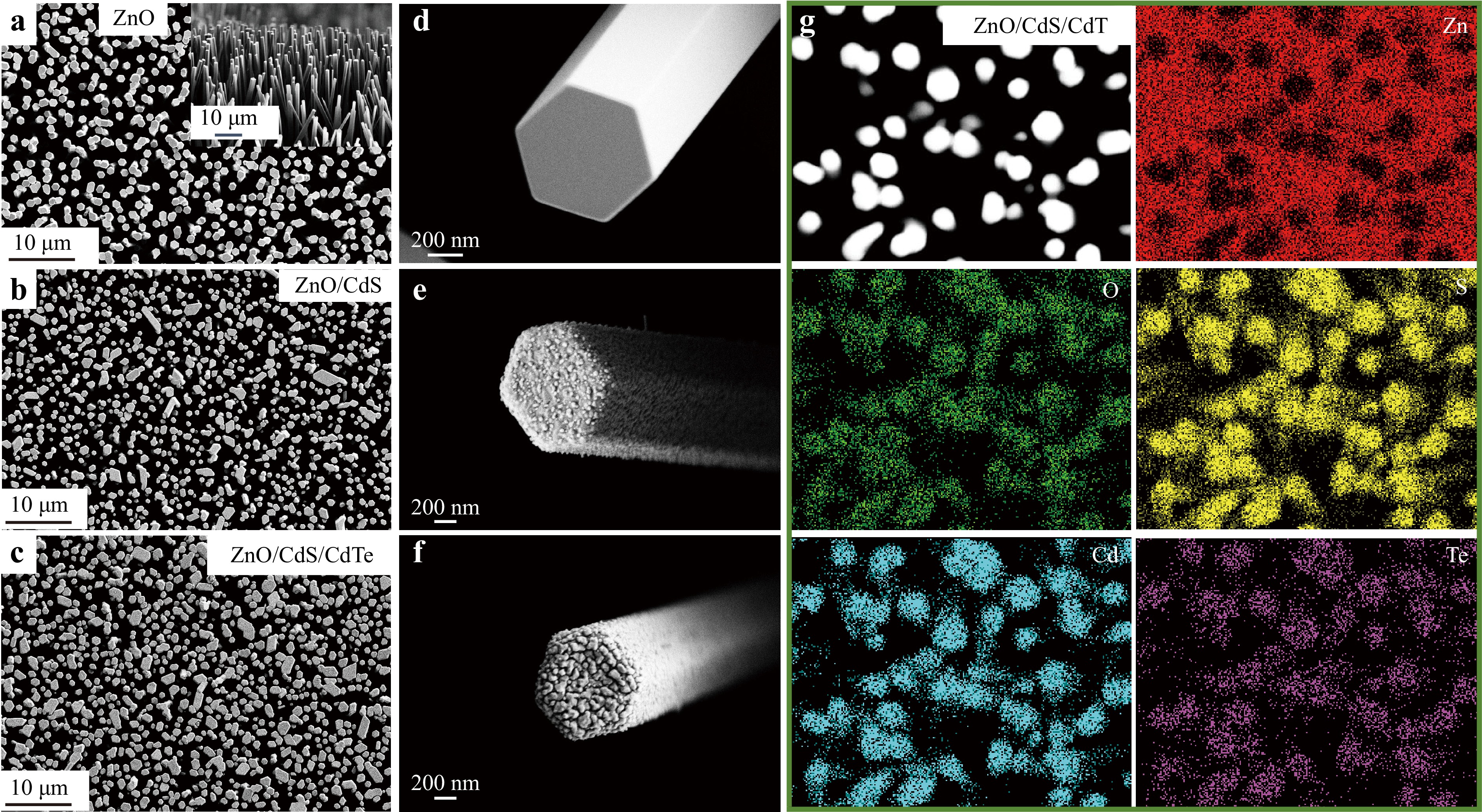
Fig. 2 a–c SEM top view pictures of well-oriented ZnO, ZnO/CdS, and ZnO/CdS/CdTe NR arrays. The inset picture is the cross-sectional view SEM image of ZnO NRs array. d–f SEM pictures of individual ZnO, ZnO/CdS, and ZnO/CdS/CdTe NR. g Elemental mappings of Zn, O, S, Cd, and Te corresponding to ZnO/CdS/CdTe NRs array.
The detailed morphologies and structures of the ZnO/CdS and ZnO/CdS/CdTe core/shell NR were characterised using TEM. The TEM image in Fig.3a shows a smooth ZnO NR with a diameter of approximately 500 nm. In the HRTEM image in Fig. 3b, the lattice distance with 0.26 nm ascribed to the (002) plane of hexagonal ZnO indicates that the ZnO NR has a high-quality single-crystal structure31. Fig. 3c shows a representative TEM image of a single ZnO/CdS core/shell NR. The CdS shell layer is regularly adorned on the ZnO NR surface. Distinct and steep interface boundaries between the ZnO core and CdS shell layer can be identified. In Fig. 3d, the lattice distance was approximately 0.34 nm, which is related to the (002) plane of hexagonal CdS32. As shown in Fig. 3e, f, the outer CdTe shell is uniformly deposited on the
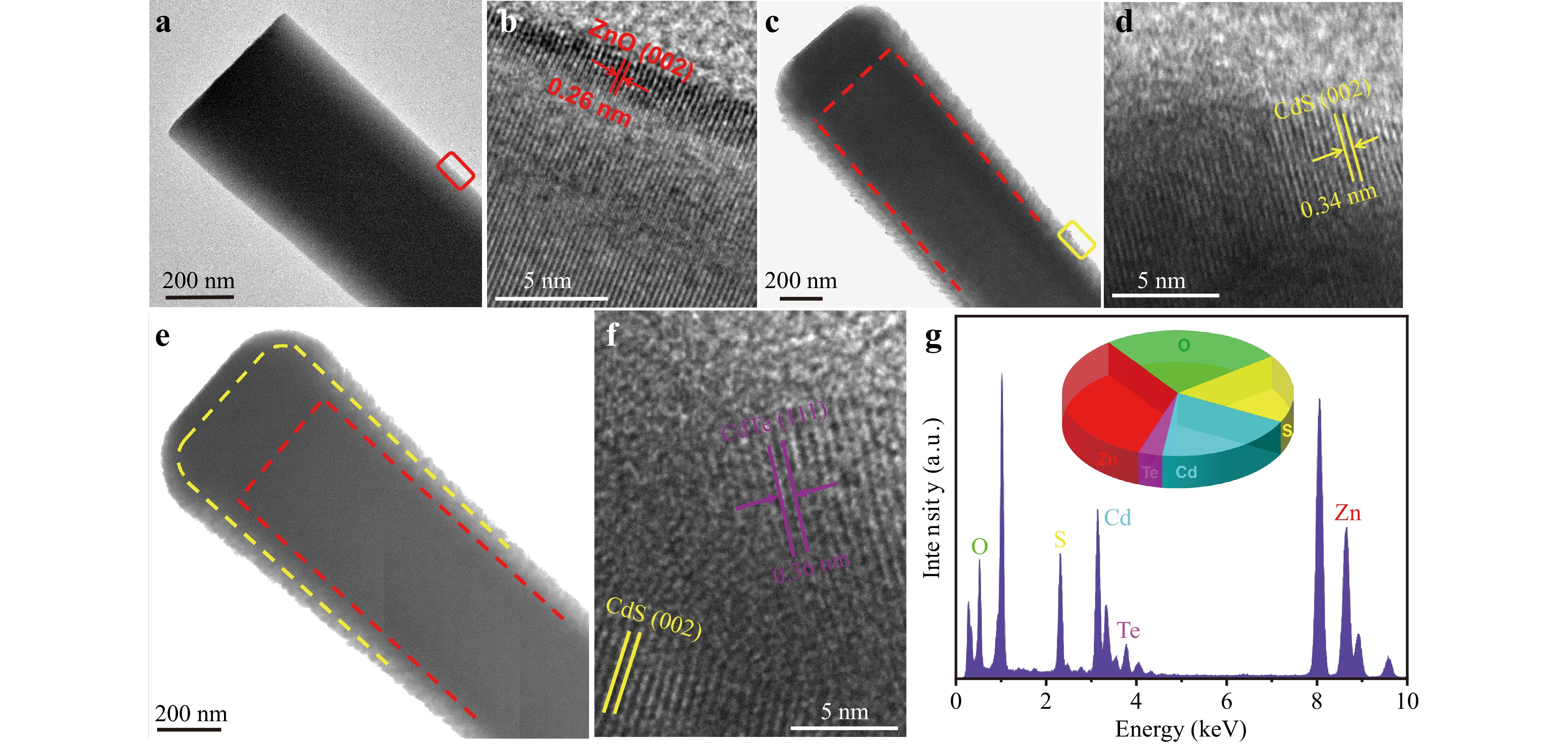
Fig. 3 a,c,e TEM images of a single ZnO, ZnO/CdS, and ZnO/CdS/CdTe NR, respectively. b,d,f High-resolution TEM images corresponding to a,c,e. g EDS spectrum of the coexistent Zn, O, S, Cd, and Te inserted with the pie chart of elements ration.
inner CdS shell. The lattice distance of 0.35 nm can be ascribed to the (111) plane, which exhibits a highly crystalline structure of CdTe33,34. The elemental contents of the coexisting Zn, O, S, Cd, and Te in the NR were identified by EDS and the pie chart in Fig. 3g, indicating the accurate components of the ZnO/CdS/CdTe NR. Furthermore, the elemental distribution in the core/shell NR was confirmed by EDS mapping. The elemental maps of Zn, O, S, Cd, and Te in a single ZnO/CdS/CdTe NR graphically prove the geometrical structure and compositional distributions of the core/shell NR heterostructure, as shown in Fig. 4a–f. Additionally, the radial and axial EDS line scan data in Fig. 4g, h demonstrate that CdS and CdTe are uniformly and orderly coated on the ZnO surface, thus generating perfect radial and axial heterojunctions. The ternary core/shell heterojunction structure revealed that the three semiconductors coexisted and combined tightly with each other, which could not only induce synergistic effects but also realise the regulation of the radial components and energy-band configuration.
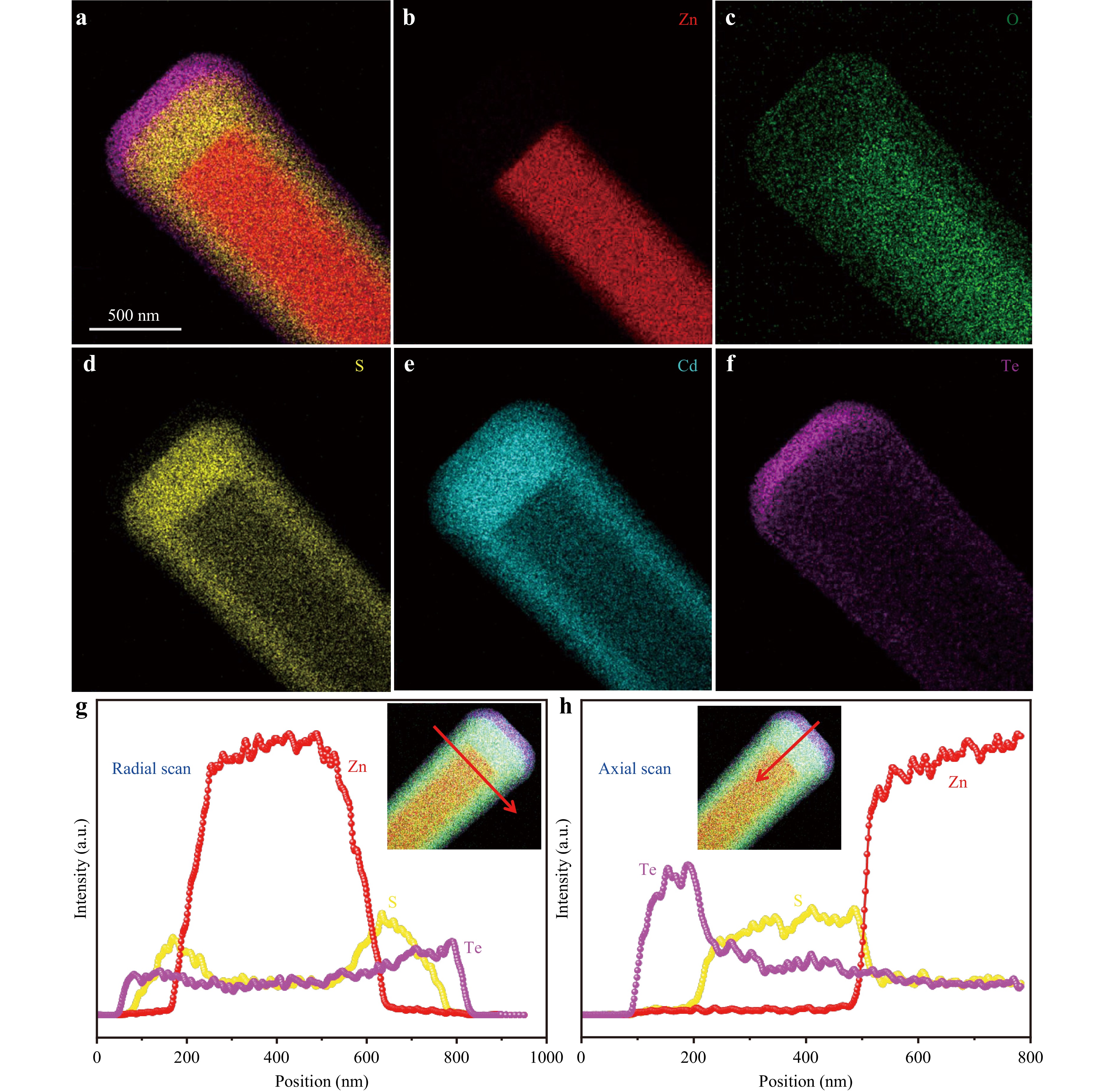
Fig. 4 a−f The EDS mappings of Zn, O, S, Cd, and Te in an individual ZnO/CdS/CdTe core/shell NR. g, h The corresponding radial and axial EDS line scanning data.
-
In the XRD pattern (Fig. 5a), the two distinct peaks at 31.08° and 34.47° can be accurately indexed to the (100) and (002) diffraction planes of hexagonal ZnO, respectively, whereas the characteristic peak at 26.56° corresponds to the (002) plane of hexagonal CdS32. After the CdTe layer coating, the new diffraction peak observed at 24.02° can be attributed to the (111) planes of CdTe35,36. These sharp peaks indicate that the heterostructured materials have good crystal quality. Additionally, Raman spectra were measured, as shown in Fig. S1. The sharp peaks of the Raman spectra also indicate that all the materials are crystalline. The elemental compositions of the ZnO, ZnO/CdS, and ZnO/CdS/CdTe NR arrays were further analysed using XPS (Fig. 5b, c). The XPS spectrum indicated that the ZnO/CdS/CdTe core/shell heterostructure contained only Zn, O, S, Cd, and Te, without any other elements, in accordance with the EDS measurements. As shown in Fig. 5d, the O 1s spectrum of pristine ZnO can be fitted to three curves, with peaks at approximately 530.6, 531.9, and 533.2 eV, respectively. The typical peak at 530.6 eV is associated with the lattice oxygen (OL) in the Zn−O bonds while the peak at 531.9 eV is ascribed to the oxygen vacancy (OV)37,38. The peak at 533.2 eV is attributed to adsorbed oxygen (OA) on the ZnO surface. As shown in Fig. 5e, after coating CdS shell layer, the OV peak of ZnO/CdS disappeared, indicating that the oxygen defects were passivated. The observed blue shifts of OL and OA were attributed to the newly formed Cd-O bond and the adsorbed CO32- and OH-, respectively39. In Fig. 5f, the Zn 2p spectrum demonstrates that the peaks at 1022.6 and 1045.8 eV belong to Zn 2p3/2 and Zn 2p1/2, respectively. Fig. 5g, h show that the unique peaks of S 2p at 162.9 and 161.7 eV belong to S 2p1/2 and S 2p3/2, and two obvious peaks at 412.2, 405.4 eV are indexed to Cd 3d3/2 and Cd 3d5/2. Two specific peaks at 582.6 and 572.1 eV correspond to the Te-Cd bond while two distinctive peaks at 586.1 and 575.7 eV belong to the Te-O bond40.
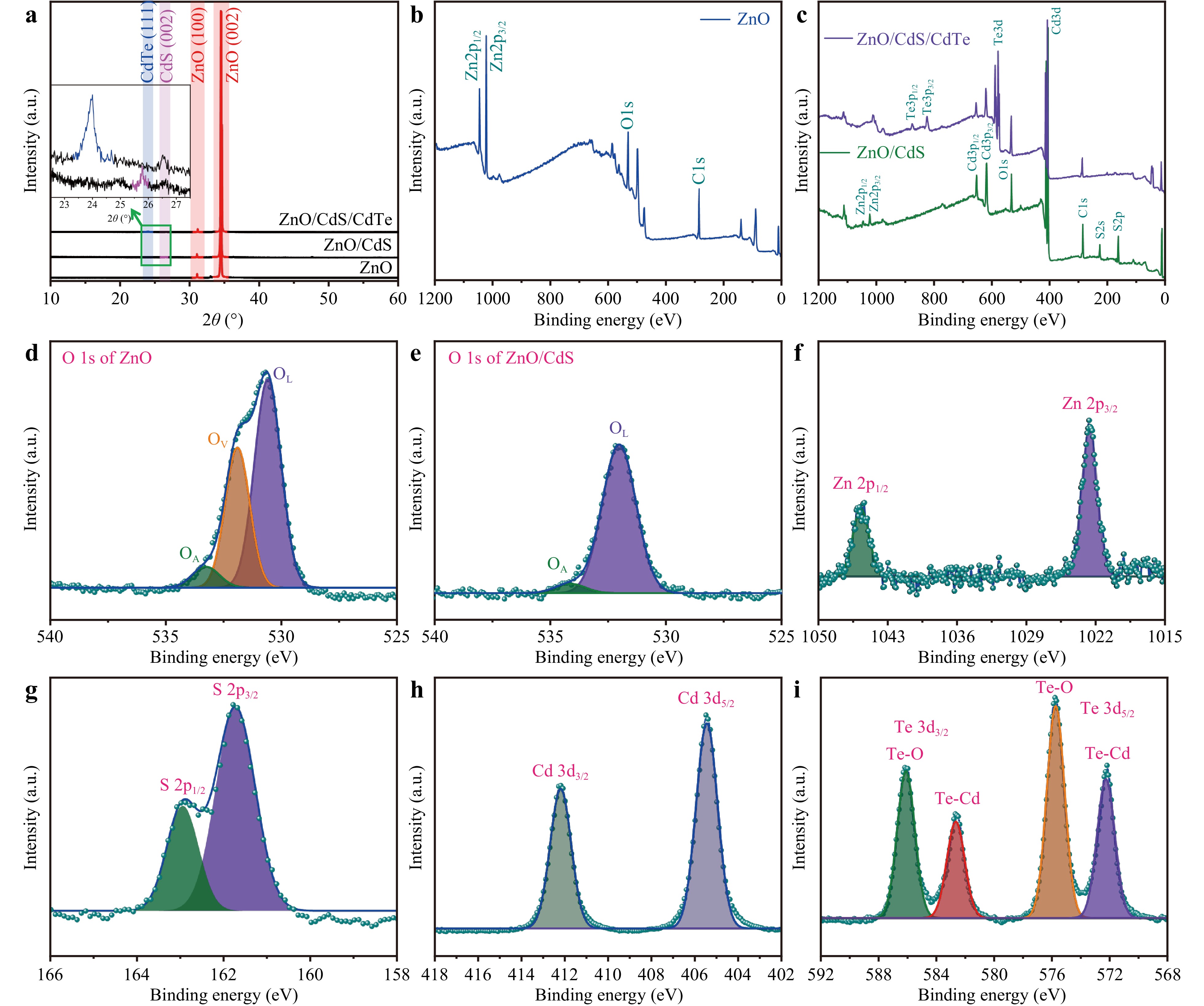
Fig. 5 a XRD pattern of ZnO, ZnO/CdS, and ZnO/CdS/CdTe NR arrays. b, c XPS survey spectra of ZnO, ZnO/CdS and ZnO/CdS/CdTe NR arrays. d, e XPS high-resolution O 1s spectrum of the ZnO and ZnO/CdS NR arrays, respectively. f–i High-resolution XPS spectra of Zn 2p, Cd 3d, S 2p, and Te 3d corresponding to ZnO/CdS/CdTe.
-
The electrical properties of the pure ZnO NR array PD were characterised. Fig. 6a exhibits the symmetrical I−V relationship in a dark environment and under the 325 nm UV light with an applied voltage between −5 and 5 V, indicating the formation of good ohmic contact. A light-to-dark current ratio (Ilight/Idark) as low as 1.92 at 5 V suggests a low photocurrent and high dark current of the pure ZnO NR arrays PD. Fig. 6b shows the time response under UV irradiation with periodic turning on and off. After 10 on/off switching cycles, a slight reduction in the photocurrent proved that the device was unstable. Owing to the durable photoconductive effect of the bare ZnO, the current was larger in the time-dependent photoresponse. Furthermore, as shown in Fig. 6c, the bare ZnO NR arrays PD exhibits a prolonged rise time (defined as the elapsed time of the signal rising from 10 to 90%) of 4.96 s, and a decay time (the elapsed time of the signal decaying from 90 to 10%) of 6.22 s41. The long rise and decay times indicate the slow response of the bare ZnO NR arrays UV PD, which was caused by the adsorption and desorption of oxygen molecules on the ZnO surface as well as the presence of numerous defects that hindered carrier transfer.
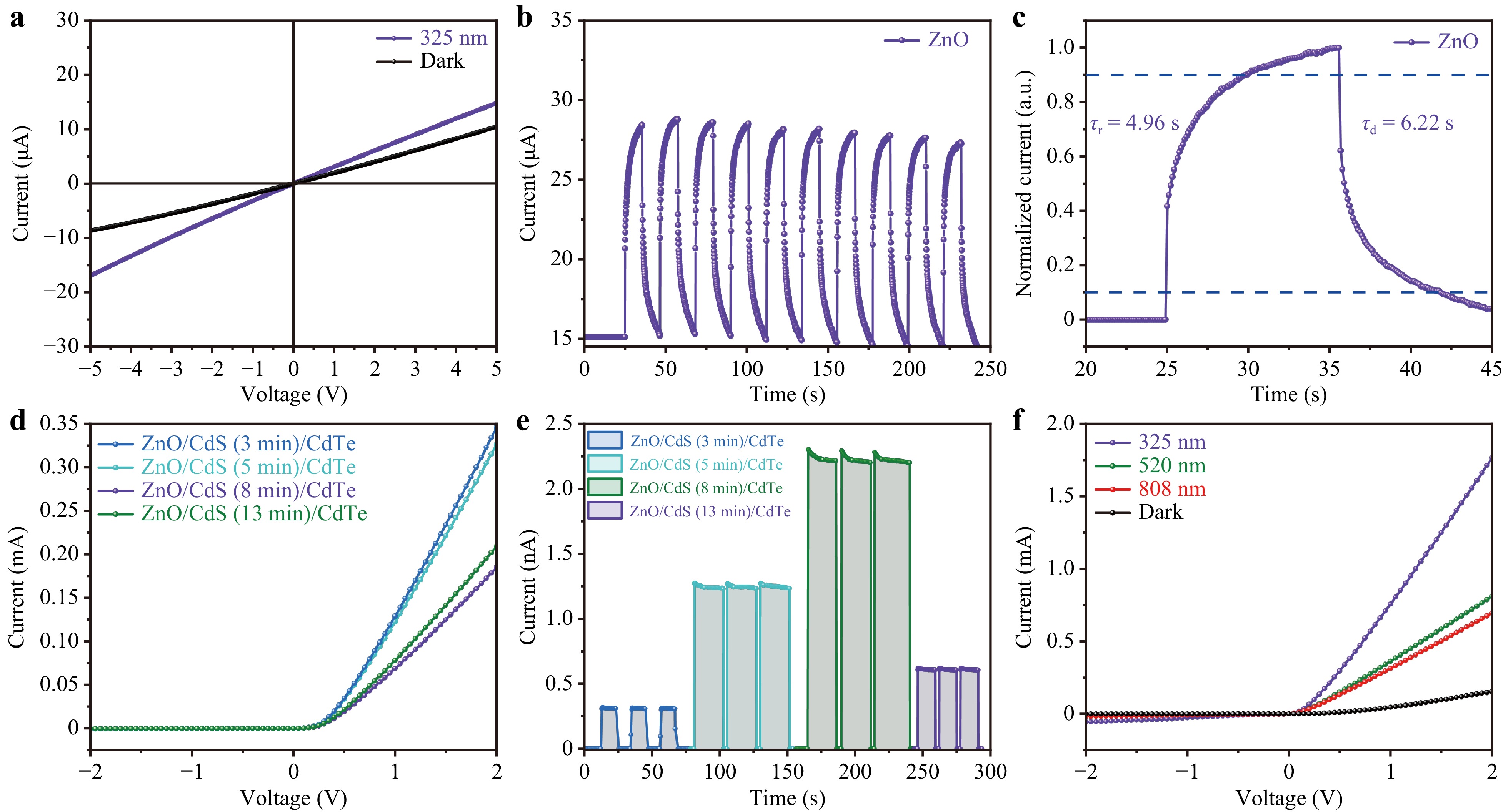
Fig. 6 a I–V plot of ZnO PD in dark environment and under the 325 nm UV illumination. b Corresponding time dependent photoresponse at 5 V. c–f Rising and falling edges for estimating the rise time and fall time of ZnO PD. d, e Dark currents and I–t plot of ZnO/CdS/CdTe NR arrays PDs with different sputtering time of CdS layer, respectively. f I–V characteristic ZnO/CdS (8 min)/CdTe NR arrays PD under dark, 325, 520, and 808 nm irradiation with 0.43 mW/cm−2.
In a cascade type-II heterostructure, the visible-light response layer of the CdS shell can also act as a charge-carrier transport layer in the ZnO/CdS/CdTe NR arrays PD. Note that optimising the thickness of the CdS layer is crucial for enhancing the performance of heterojunction PD. For a PD, a low dark current and high Ilight/Idark ratio are important for improving the weak light detection performance and antinoise ability. Hence, the dark currents of ZnO/CdS/CdTe NR arrays PDs with different CdS sputtering times were measured, as shown in Fig. 6d. This rectifying behaviour confirmed that the p–n junction was well formed at the ZnO/CdS/CdTe heterointerface. As the CdS sputtering time increased to 8 min, the dark current gradually decreased, but then increased when the sputtering time reached 13 min. In addition, I−t curves of different PDs with a different sputtering time of CdS were analysed, as presented in Fig. 6e. The PD with an 8 min sputtering time of the CdS layer shows the highest Ilight/Idark of approximately 104. Therefore, the ZnO/CdS (8 min)/CdTe core/shell NR arrays PD maintained the lowest dark current, and the highest Ilight/Idark ratio resulted in the best broadband photodetection performance. These phenomena indicate that a CdS layer that is too thin (3 and 5 min) cannot form a high-quality shell layer, which is unfavourable for the effective transportation of charge carriers. In contrast, a thicker CdS layer (13 min) increased the transportation distance and promoted the consumption and recombination of charge carriers. Subsequent studies were based on ZnO/CdS (8 min)/CdTe core/shell NR arrays PD. To further investigate the specific photoresponse to UV–Vis–NIR, typical I–V characteristics were measured in the dark and under 325, 520, and 808 nm irradiation with 0.43 mW/cm-2, as presented in Fig. 6f.
Fig. 7a–c exhibit the time responses of the ZnO/CdS/CdTe NR arrays PD under 0 V bias, with light illumination of 325, 520, and 808 nm switched on/off, respectively. The 10 periodical on/off switching cycles demonstrate that the device maintains good stability and reproducibility, and the photocurrents are 7.79, 1.78, and 0.32 nA under 325, 520, and 808 nm irradiation with 0.43 mW/cm2, respectively. Fig. 7d–f illustrate the photoresponse speed and photodelay by enlarging the rising and decaying edges of the photoresponse curves. The rising/decaying times are 0.6/1.8 s for 325 nm UV light, 0.3/0.5 s for 520 nm visible light, and 0.7/1.6 s for 808 nm NIR light, respectively. Notably, in our 1D core/shell PD, the designation of top-bottom electrodes would lead to a long charge-carrier transportation distance and promote the consumption of charge carriers, thus resulting in long rise time and fall time. Additionally, the continuous light source with low power would aggravate the durative photoconductive effect, which can make the rise time and fall time larger. Fig. 7g–i present the time-dependent response of ZnO/CdS/CdTe core/shell NR arrays PD illuminated under 325, 520, and 808 nm by changing light power densities. The electron–hole pairs generation rate depends mainly on the light intensity. The photocurrent rises as light power density increases, and the on/off ratio reaches the maximum under 0.71 mW/cm2. As demonstrated in the inset pictures, the power law of I∝Pk can be used to fit the function between photocurrent and excitation power density, in which I represents the photocurrent, P represents power density, and k is the empirical value42. The fitted curves indicate that the values of k are 0.85 for 325 nm, 0.86 for 520 nm, and 0.85 for 808 nm. Such high values of k suggest that the vertically aligned core/shell PD possesses fewer defects and can adsorb more incident light.
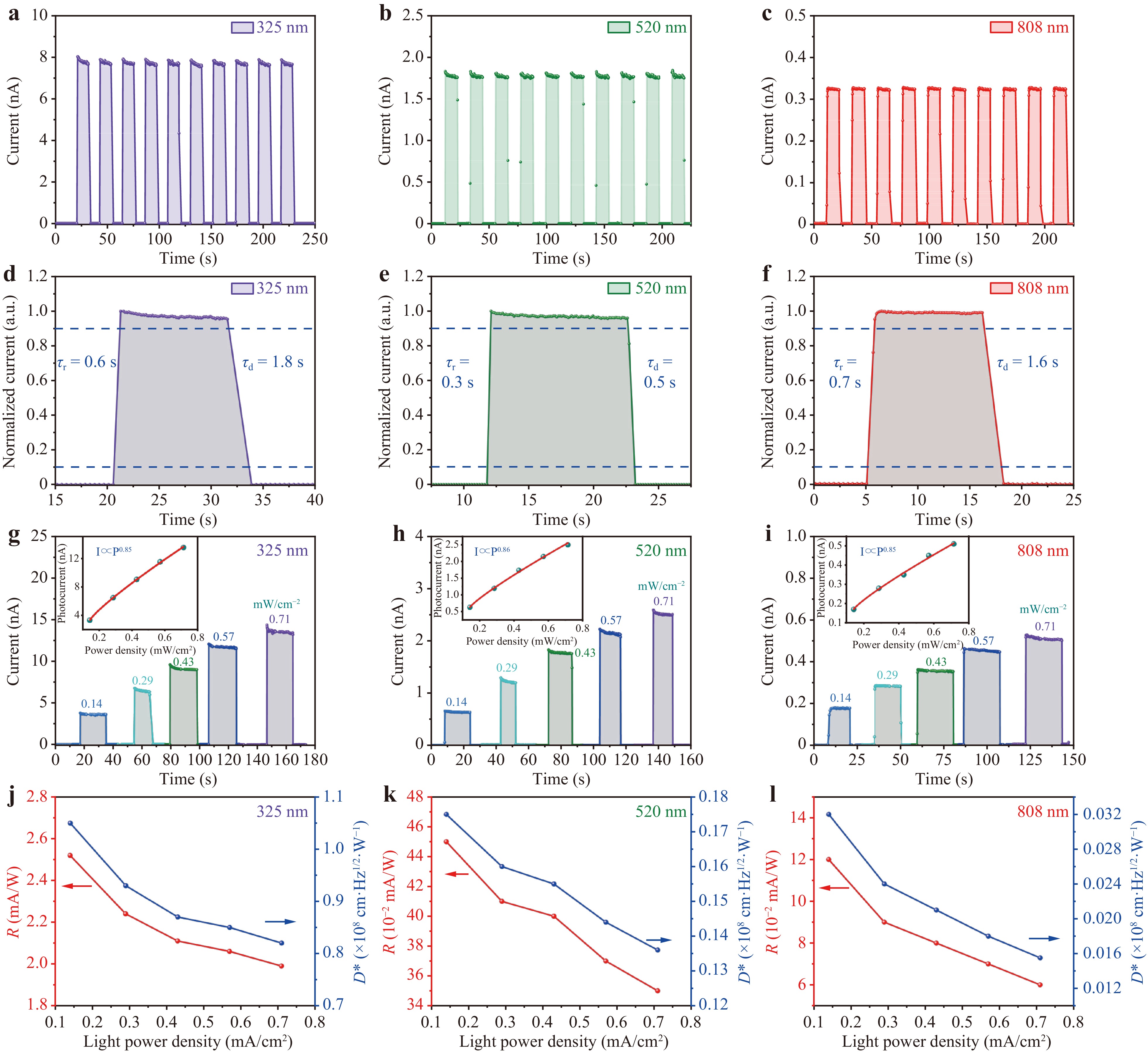
Fig. 7 a–c Time responses of the ZnO/CdS/CdTe NR arrays PD with 325, 520, and 808 nm light irradiation switched on and off under 0 V bias, respectively. d–f Rising and falling edges for estimating the rise time and fall time, correspondingly. g–i I–t plots of ZnO/CdS/CdTe NR arrays PD under 325, 520, and 808 nm irradiation with different light power densities, and the inset pictures show the photocurrent as a function of power densities. j–l Dependence of responsivity and detectivity of the device with light power density under 325, 520, and 808 nm.
Generally, the responsivity (R) and detectivity (D*) are key parameters for investigating the performance of a PD. D* represents the signal-to-noise ratio generated by each unit of irradiation power of the PD under a unit bandwidth and area, which can be evaluated by the capability of the PD to detect weak light. It is a comprehensive indicator and cannot be calculated through the dark current (based on shot noise), which may result in an overestimation compared to the true value43,44. Therefore, R and D* are defined as follows:
$$ R = \frac{{{I_{{\text{light}}}} - {I_{dark}}}}{{PS}} $$ $$ D* = \frac{{\sqrt {S\Delta f} }}{{NEP}} , $$ $$ NEP = \frac{{In}}{R} , $$ When the PD responds at a high frequency, the device noise In can be estimated from the white noise of the thermal noise and shot noise using the following formula:
$$ I_n = \sqrt {2qI_{dark}\Delta f + \frac{{4k_BT}}{{R_d}}\Delta f} $$ Here, P, S, and q are the light power density, effective light area, and electric charge, respectively45. Δf (Hz) is the electrical bandwidth of the noise measurement, noise-equivalent power characterizes the smallest optical signal power that can be resolved from PD noise, In is the noise current, kB is the Boltzmann constant, and Rd = dV/dI is the resistance44,46. Based on the above equations, under 0.43 mA/cm2 illumination density excitation, the R and D* were 2.11 mA/W and 0.87 × 108 cm·Hz1/2·W−1 for 325 nm, 0.40 mA/W and 0.155 × 108 cm·Hz1/2·W−1 for 520 nm, and 0.08 mA/W and 0.021 × 108 cm·Hz1/2·W−1 for 808 nm, respectively. The dependences of R and D* on different light power densities are graphically presented in Fig. 7j–l.
-
To investigate our device evidently, the comparison of our device with some other ZnO core/shell-based PDs is shown in Table 1. Our PD has a better performance for multiwavelength detection, suggesting that the ZnO/CdS/CdTe radial core/shell heterojunction device is a promising candidate for a broadband PD. The key point is the sharp and distinctive heterointerfaces formed between the core and shell. In addition, by integrating different functional materials with a type-II energy band configuration that favours charge-carrier transportation, our device can exhibit high performance for broadband photodetection.
ZnO core/shell-based devices Bias
(V)Range of detection Responsivity Detectivity
(cm·Hz1/2·W−1)Rise/decay time References ZnO/SnO2 1 UV 28.5 (±0.6) A/W 2.9 (±0.1) × 1014 8.7/20.8 s 26 ZnO/ZnMgO 5 Dual-UV − − 4.186/1.217 s
4.352/1.397 s27 ZnO-Co3O4 0.1 Vis 21.8 mA/W 4.12 × 10¹² 6 s/− 25 ZnO-Cu2O 0 Vis 7.74 μA/W − ≤0.09 s 13 ZnO/CuCrO2 −1 UV 8.87 mA/W 8.5 × 10⁹ 32/35 μs 7 ZnO/CdS/CdTe 0 UV
Vis
NIR2.11 mA/W
0.40 mA/W
0.08 mA/W0.87 × 108
0.155 × 10⁸
0.021 × 1080.6/1.8 s
0.3/0.5 s
0.7/1.6 sThis work Table 1. Comparison of the performance of ZnO core/shell-based photodetectors with existing literature.
To further understand the carrier behaviour in the radial core/shell heterojunction, the absorption spectra of the ZnO, ZnO/CdS, and ZnO/CdS/CdTe NR arrays are shown in Fig. 8a. The strong absorption edge of pure ZnO was at approximately 380 nm, which is in accordance with the intrinsic bandgap of 3.3 eV. After introducing the CdS shell layer, the ZnO/CdS NRs array displayed significant absorption in the visible light region, suggesting a robust visible light response. For the ZnO/CdS/CdTe NR arrays, the absorption edge extended further into the NIR region, followed by the deposition of CdTe. Therefore, the results suggest that the ZnO/CdS/CdTe core/shell NR arrays maintains a broadband photoresponse from the UV to the Vis and NIR wavelengths. The PL spectra were used to study the separation and transition of the photoexcited carriers. As shown in Fig. 8b, the UV emission peak located at 380 nm in the pure ZnO NR arrays is ascribed to intrinsic emission, whereas the visible emission is attributed to defective emission. The broad PL peak located at approximately 525 nm is the most commonly observed defect emission in ZnO and is attributed to oxygen vacancies47,48. Compared with bare ZnO, the UV emission intensities of ZnO/CdS and ZnO/CdS/CdTe decreased significantly, indicating efficient separation of the photoexcited carriers. Notably, the distinct quenching of the defective luminescence indicates that the modification of CdS and CdTe can also passivate the defects on the ZnO surface, which favours photodetection. Moreover, TRPL was used to explore the charge-carrier transfer performance, as shown in Fig. 8c. A single exponential decay function of I (t)= A1exp (-t/τ) +I0 can be used to fit the normalised TRPL decay curves. The τ values for ZnO, ZnO/CdS, and ZnO/CdS/CdTe were 512, 419, and 251 ps, respectively, indicating that the fluorescence lifetime decreased with shell layers coating. These results suggest that, after introducing CdS and CdTe shell layers, the core/shell heterostructures can form stepped type-II energy band alignment can effectively promote the electron−hole pairs separation and efficiently facilitate the carriers' transfer.
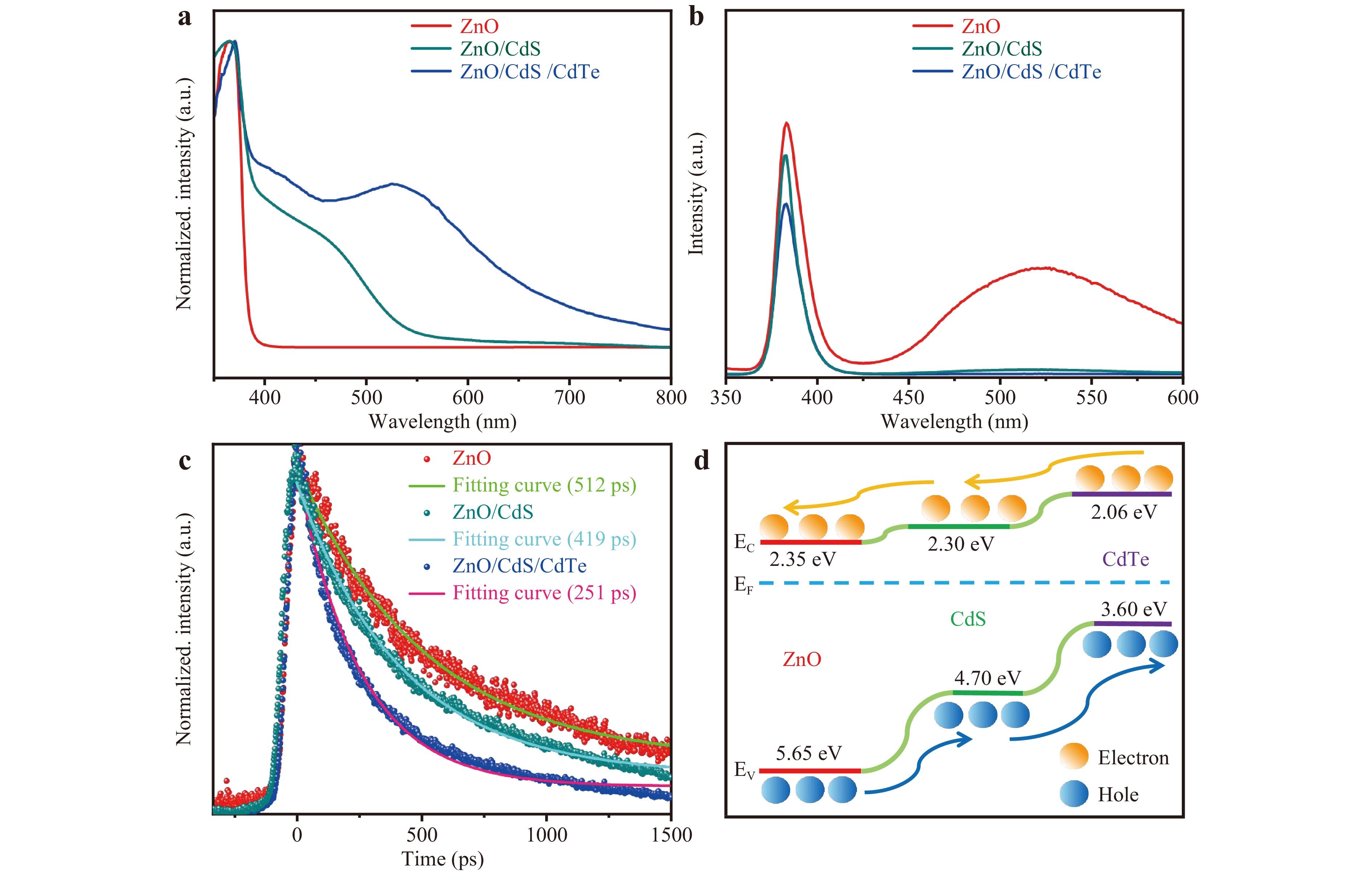
Fig. 8 a UV−Vis diffuse reflectance spectra of ZnO, ZnO/CdS, and ZnO/CdS/CdTe NR arrays. b,c The PL spectra of ZnO, ZnO/CdS, and ZnO/CdS/CdTe NR arrays. (c) TRPL spectra of ZnO, ZnO/CdS and ZnO/CdS/CdTe NR arrays. d Energy-band diagram of the ZnO/CdS/CdTe NR arrays heterojunction.
The rapid response of the ZnO/CdS/CdTe NR arrays PD can be attributed to the distinct core/shell radial heterointerface and well-organised cascade type-II energy band alignment. By sputtering shell layers on ZnO, surface oxygen absorption can be suppressed, and the surface defect states can be passivated. In the heterostructure, the high crystallisation quality of the shell layers and distinct junction interfaces guarantee photoelectric performance, whereas the cascade type-II energy band alignment promotes effective charge carrier separation and transition. Moreover, dual heterojunctions increase the width of the depletion layer, and more electrons can be depleted, thus reducing the dark current.
To gain insight into the operational principle of the self-powered ZnO/CdS/CdTe core/shell NR arrays broadband PD, Fig. 8d shows the energy-band diagram of the radial heterojunction and the transport processes of the photogenerated carriers49. The Fermi level, valence band minimum, and conduction band minimum positions of each material were calculated based on the UPS spectra shown in Fig. S2. Such a stepped energy-band configuration can accelerate the transport of photogenerated charge carriers from the ZnO core to CdS and CdTe. Under 325 nm illumination, the photon energy of UV (3.82 eV) is higher than that of ZnO (3.30 eV), CdS (2.40 eV), and CdTe (1.54 eV). Therefore, all of them can generate electron–hole pairs, leading to the best photoresponse. Holes migrate from ZnO to CdS and CdTe and then to the Ag electrode, while electrons transfer from ZnO to the Au electrode, facilitating charge separation and transmission. When irradiated by 520 nm visible light, electron-hole pairs are mainly generated in both CdS and CdTe. Holes were transferred to CdTe, whereas electrons were transferred to ZnO by the built-in electric field. Similarly, in the case of 808 nm NIR detection, the photogenerated charge carriers are only excited in CdTe. The holes in the valence band of CdTe are transferred to the Ag electrode, whereas the electrons are transferred steadily to ZnO. Owing to the well-matched band energy levels and distinctive interface, broadband detection without external bias was possible based on the photovoltaic effect.
In summary, 1D core/shell structures can provide a spatially confined carrier transport channel, reducing charge scattering and enhancing light field confinement, thereby improving optical absorption efficiency. By integrating the functional materials of the CdS and CdTe shell layers on the ZnO core, the 1D ZnO/CdS/CdTe core/shell radial heterojunction PD can realise broadband photodetection from UV to Vis and NIR wavelengths. A high-quality interface with a cascade type-II energy band alignment could contribute to a more stable carrier transfer and reduce energy loss. This design facilitates effective photogenerated charge-carrier separation, resulting in an enhanced photoresponse. Additionally, by optimising the thickness of the CdS shell layer, the 1D ZnO/CdS/CdTe core/shell heterojunction PD exhibited superior photoresponse under 325-, 520, and 808 nm irradiation at a 0 V bias. The R and D* were 2.11 mA/W and 0.87 × 108 cm·Hz1/2·W−1 for 325 nm, 0.40 mA/W and 0.155 × 108 cm·Hz1/2·W−1 for 520 nm, and 0.08 mA/W and 0.021 × 108 cm·Hz1/2·W−1 for 808 nm, respectively. This study provides a reliable and universal technique for the design and fabrication of novel core/shell nano-optoelectronic devices. However, the lack of reliable electrodes limited the detection performance in our study. In the future, realizing the convenient and reliable fabrication of electrodes is hopeful to develop a new type of device for on-chip optical transceivers, deep space exploration, and other important applications.
-
First, a 99.99% pure ZnO target was sputtered onto a cleaned Si/SiO2 substrate to obtain a ZnO seed layer under 80 W, for 30 min. Next, a ZnO NRs array was fabricated using CVD. An equal mass ratio of the ZnO and graphite powder mixture was placed at the end of the quartz tube. Subsequently, a substrate with a sputtered ZnO seed layer was put into the nozzle and followed by heating at a high temperature (1050 ℃) with oxygen and argon (15:150 sccm) as the carrier gases for approximately 30 min. Third, the inner shell layer of CdS was sputtered onto the ZnO NRs surface via magnetron sputtering with 99.99% purity of the CdS target, 2.0 Pa working pressure, 55 sccm Ar flow, and 80 W sputtering power. The thickness of the CdS layer depended on the sputtering time. Hence, to optimise the thickness of the CdS layer, the sputtering time was varied as 3, 5, 8, and 13 min. Fourth, the CdTe shell layer was grown on the ZnO/CdS core/shell surface by RF magnetron sputtering with similar parameters (99.99% purity of CdTe target) for 5 min. Finally, the bottom electrode of the broadband PD was constructed by depositing Au on the ZnO layer through thermal evaporation, followed by spin-coating the Ag nanowires on the ZnO/CdS/CdTe NR arrays as a top contact electrode.
-
The microstructures of the ZnO, ZnO/CdS, and ZnO/CdS/CdTe NR arrays were observed using a Carl Zeiss SEM. The crystal structures were resolved by TEM on an FEI Talos F200X instrument equipped with an EDS spectrometer to track the elemental composition. The phase and chemical composition were determined using X-ray diffraction (XRD, Ultima IV) and X-ray photoelectron spectroscopy (XPS, Thermo Scientific K-Alpha), respectively. The electrical properties of the devices were measured using a semiconductor parameter system (Keithley 4200). Room-temperature photoluminescence (PL) spectra were recorded using an optical multichannel analyser (Acton SP2500i). The size of the photosensitive area was 0.01 cm2. A streak camera (Optronis Optoscope ) equipped with a 325 nm femtosecond pulsed laser was used to record the time-resolved PL (TRPL) spectrum.
-
This work was supported by the National Natural Science Foundation of China NSFC (62075041, 62375049, 62335003), and the Basic Research Program of Jiangsu Province (BK20222007)
One-dimensional core/shell radial heterojunction with cascade type-II energy-band alignment for enhanced broadband photodetection
- Light: Advanced Manufacturing , Article number: (2024)
- Received: 10 November 2023
- Revised: 12 July 2024
- Accepted: 12 July 2024 Published online: 24 September 2024
doi: https://doi.org/10.37188/lam.2024.040
Abstract: Constructing a one-dimensional (1D) core/shell heterostructure is a rational and efficient way to integrate multiple functional materials into a single device, in which a distinct and reliable interface and suitable energy-band alignment play important roles in optoelectronic applications. Here, using a typical magnetron sputtering system, we constructed a 1D ZnO/CdS/CdTe core/shell nanorod arrays radial heterojunction with a well-designed cascade type-II energy band alignment and improved the broadband photodetector (PD) performance. The well-formed shell layers compensated for the defect states on the ZnO surface and extended the photoresponse range from ultraviolet to visible and near-infrared. Moreover, reliable and distinct heterointerfaces with a cascade type-II energy band alignment can guarantee more stable carrier migration and reduce energy loss, promoting effective photogenerated charge carrier separation and resulting in an enhanced photoresponse. The optimised 1D ZnO/CdS/CdTe core/shell heterojunction PD exhibited a fast photoresponse at 0 V bias with high responsivity and detectivity. These results provide an important reference for the rational design and controllable synthesis of multifunctional optoelectronic nanodevices.
Research Summary
one-dimensional core/shell structure for broad-spectrum photodetection
A Highly ordered one-dimensional (1D) semiconductor nanostructures with larger specific surface area and better light-absorbing properties have significant advantages in constructing high-performance integrated optoelectronic devices. By choosing different functional materials and constructing core/shell radial heterojunctions, flexible adjustment of the energy-band and high functional integration can be realized. A research team led by Prof. Chunxiang Xu at Southeast University has made new progress in the field of broad-spectrum photodetectors with 1D core/shell radial heterostructures. They constructed 1D ZnO core/shell radial heterojunctions with clear interfaces through the classical magnetron sputtering technique, which effectively passivated the surface defects of 1D ZnO and suppressed the sustained photoconductivity effect of the device. At the same time, a rationally designed cascade type-II energy-band arrangement promotes the separation and transport of photogenerated carriers, which substantially improves the detection performance of the device and realizes a broad spectral detection from the ultraviolet to the visible and the near infrared.
Rights and permissions
Open Access This article is licensed under a Creative Commons Attribution 4.0 International License, which permits use, sharing, adaptation, distribution and reproduction in any medium or format, as long as you give appropriate credit to the original author(s) and the source, provide a link to the Creative Commons license, and indicate if changes were made. The images or other third party material in this article are included in the article′s Creative Commons license, unless indicated otherwise in a credit line to the material. If material is not included in the article′s Creative Commons license and your intended use is not permitted by statutory regulation or exceeds the permitted use, you will need to obtain permission directly from the copyright holder. To view a copy of this license, visit http://creativecommons.org/licenses/by/4.0/.

 DownLoad: