


-
In nature, two types of exquisite and outstanding optical systems exist: the vertebrate eyes and insect compound eyes (CEs). The former type of eye (e.g. human eyes) is a single-aperture optical system, in which incident light can be collected and focused by a tunable lens onto the retina.1, 2 By contrast, the latter type of eyes (e.g. the CEs of a dragonfly) are multi-aperture systems comprising thousands of individual photoreception units (ommatidia) closely arranged on a hemispherical surface (main eye). Generally, vertebrate eyes are capable of zoom and high-resolution imaging, whereas the view angle is limited. By contrast, CEs feature a wide field-of-view (FOV), dynamic target detection ability, and an infinite field depth3-6. Compared with vertebrate eyes, CEs of relatively small size and low system complexity are more suitable for cutting-edge applications in robotic vision, panoramic imaging, aircraft navigation, and military reconnaissance7-17. Consequently, artificial CEs (ACEs) have garnered significant attention in the development of advanced optical systems.
Generally, ACEs can be classified into two different types based on their device structures: (i) macroscopic multicamera array7-11, and (ii) integrated CEs12-17. The former type comprises several or dozens of single-aperture commercial cameras, serving as ommatidia. Because those cameras are commercially available, such CE systems can be established easily. Consequently, innovations are primarily focused on the analysis and reconfiguration of images obtained from those cameras. For example, Wilburn et al. presented a custom video system of a planar 10 × 10 camera array7. By combining different lenses of the camera system, multiple configurations such as high-resolution imaging and high-speed video capture can be easily realised. To further enlarge the FOV of ACEs, cameras can be arranged on a hemispherical surface, imitating the geometries of natural CEs, such as a panoptic camera system comprising 30 cameras, as demonstrated by Afshari,8, 9 and the AWARE-2 camera with an FOV of 120° × 50° presented by Brady10. The latter type is an integrated CE comprising an integrated multi-aperture system including a microlens array (MLA) and an image sensor array. Each microlens can serve as an ommatidium. For example, Jeong et al.18 fabricated a close-packed MLA on a hemispherical dome with a diameter of 2.5 mm, including 8370 microlenses. Wu et al.19 successfully presented a three-dimensional (3D) 84-μm CE with 150 ommatidia, which is similar to the natural ant CE. These compact MLAs have created new opportunities for the development of advanced ACE cameras.
In the past decades, ACEs based on multicamera arrays have enabled high-resolution, panoramic, and 3D imaging. However, considerable difficulties arise in miniaturisation owing to the large size of commercial cameras. Integrated CEs offer potential for miniaturisation considering their small MLA size, which is typically from tens of microns to several centimetres, and their image-coupled sensor. In particular, with the rapid progress of nanofabrication technologies, 3D MLAs with complex configurations can be readily manufactured for developing advanced ACE systems. Notably, the resultant miniature ACEs demonstrate unique features, including small dimensions, portability, large FOV, high sensitivity, and 3D imaging capability. Accordingly, such ACEs have garnered research interest as an advanced optical system for potential applications in endoscopy, microrobot vision, and other integrated microsystems.
To provide a comprehensive review of miniature ACEs herein, we summarise the recent advancements in this field, emphasising particularly on state-of-the-art manufacturing technologies including photolithography-assisted shaping, strategies based on microdroplets, ultraprecision machining (UPM), and femtosecond laser manufacturing. In addition, the unique features of ACEs and their potential applications are introduced. Finally, a short perspective regarding current challenges and opportunities is discussed.
-
Unlike single-aperture lens, ACEs are MLAs that are closely packed on a curved surface, serving as a swarm of ommatidia. Their complex and delicate 3D structures render them challenging to fabricate using general technologies. Since the 1980s, various novel methods that enable the fabrication of MLAs have emerged. Initially, strategies to manufacture them were primarily based on photolithography technologies, such as the photolithography-assisted thermal reflow method, ion exchange method, and photolithography-assisted etching. In the 1990s, technologies based on microdroplets have been proposed, such as microdroplet jetting and wettability controlled microdroplet arrangement. With the development of microfabrication technologies, UPM and femtosecond laser manufacturing have been employed as advanced manufacturing processes for prototyping curved/3D MLAs. In Fig. 1 we give an overview of the fabrication techniques on a timeline.
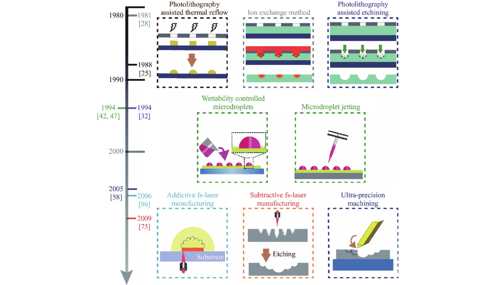
Fig. 1 Technologies for fabricating MLA and representative fabrication methods.
To date, the abovementioned technologies have contributed significantly to the development of ACEs. However, for the practical application of ACEs, their manufacturing technologies require further improvements. To prepare high-quality ACEs, the following key aspects must be emphasised. The first is the 3D configuration of ACEs. To realise the basic functionalities of CEs, all of the ommatidia should be closely packed on a curved surface. The close-packed arrangement (100% fill factor) can ensure the complete utilisation of space light information, and the 3D distribution of ommatidia can enable large FOV imaging. Second, the surface profile and smoothness of each ommatidium that govern the imaging quality should be considered. For example, microlenses with aspherical surfaces have lower spherical aberration than spherical surfaces. In certain cases, the profile of each ommatidium should reflect a certain functional equation, instead of a simple hemisphere shape. In addition, the integration of ACEs with imaging sensors is vital to practical applications. Considering the abovementioned key aspects, technologies that enable 3D programmable fabrication are highly desired. Herein, the aforementioned requirements are considered as evaluation criteria for current technologies, and a comprehensive summary of these fabrication methods is shown in Table 1.
Manufacturing Technology Subtractive/ Additive laser manufacturing Curved surface 100% fill
factorFreeform single micro- lens Diameter of single micro-lens Size of MLA Material Ref (year) Direct Indirect Photolithography Photolithography assisted thermal reflow Subtractive laser manufacturing ○ × × 120 μm − DNR photoresist 20 (2020) 10 μm 1.5 cm × 1.5 cm Polystyrene (PS) 21 (2019) 10 μm − AZ 5214 photoresist 22 (2010) 900 μm 0.9 cm × 0.9 cm AZ 4620 photoresist 25 (2009) Photolithography and ion exchange method − ○ ○ × 100 μm D > 1.5 cm Glass 28 (2003) 20 μm D=500 μm Glass 29 (2019) Photolithography assisted etching Subtractive laser manufacturing ○ ○ × 15 μm − AZ 4620 photoresist 30 (2014) 100-400 μm ~ cm Si 31 (2009) Fabrication methods based on microdroplets Microdroplets Jetting Additive laser manufacturing ○ × × 10~100 μm − UV polymer 40 (2018) 1~20 μm − UV polymer (NOA) 43 (2020) Wettability controlled MLA 2 mm ~cm Oil droplet 44 (2015) 100 μm − Glycerol droplet 46 (2017) Ultra-precision machining Subtractive laser manufacturing ○ ○ ○ 500 μm D= 0.82 mm Glass mold 54 (2018) 1 mm 13 mm × 5 mm Hard mold 55 (2018) Femtosecond laser manufacturing Laser ablation process Subtractive laser manufacturing ○ ○ ○ 20 μm 10 mm × 10 mm Silicon glass 69 (2015) 24.5 μm D=5 mm Silicon glass 73 (2016) Two-photon absorption (TPA) Additive laser manufacturing ○ ○ ○ 5 μm D=85 μm SU8 17 (2014) 8 μm D=64 μm BSA protein 95 (2019) Table 1. Summary of advantages and disadvantages of major ACE fabrication methods.
-
Photolithography is a major micromachining technology that defines patterns utilising the chemical reaction of a photoresist to an electron beam or light of particular wavelengths20, 21. It has been widely used for manufacturing bionic CE arrays in the early stages. As a traditional planar technology, photolithography-based micromachining methods are typically limited to the manufacture of planar MLAs. Three primary processing technologies for producing planar MLAs are listed in the following section. To achieve MLAs on a nonplanar surface, several optimisation methods have been proposed for developing curved MLAs, such as changing the shape of the elastic substrate, which will be discussed later.
-
The thermal reflow process has been considered as a simple and effective method for the fabrication of large-area MLAs22-27. The fabrication process for thermal reflow is depicted in Fig. 2a. First, the photoresist coated on the substrate is exposed under ultraviolet (UV) light and forms an array of cylindrical isolated islands during lithography. Subsequently, the substrate is heated above the glass transition temperature of the photoresist. Owing to the surface tension effect, the cylindrical islands melt and transform into hemispheres to minimise the surface energy. Fig. 2b shows the morphological changes before and after thermal melting22. Thermal reflow is a simple and fast process for mass production; however, close-packed MLAs are not restricted by the mask. In addition, the morphology of the microlenses is difficult to control considering multiple factors such as the photoresist height as well as the contact angle between the substrate and photoresist; consequently, the optimal performance of MLAs may be adversely affected.
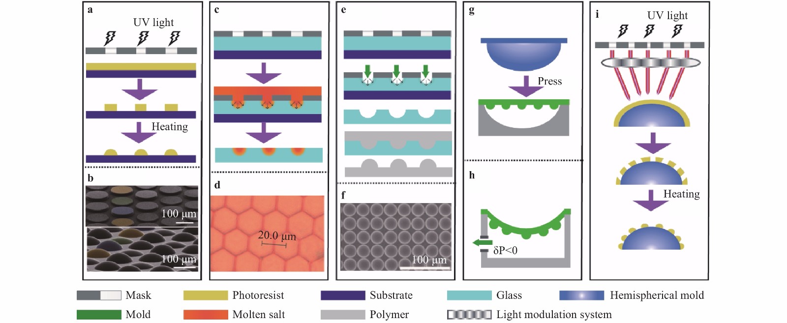
Fig. 2 Photolithography-assisted machining of MLAs.
a Schematic diagram of photolithography-assisted thermal reflow procedure. b MLA before and after thermal reflow process22. Reprinted with permission. Copyright 2020, OSA. c Schematic diagram of ion exchange procedure. d MLA based on ion exchange31. Reprinted with permission. Copyright 2019, OSA. e Schematic diagram of photolithography-assisted hot embossing procedure. f MLA based on photolithography-assisted hot embossing35. Reprinted with permission. Copyright 2020, OSA. Schematic diagram of 3D MLA fabrication via shape deformation of planar MLA under mechanical pressure g and air pressure h. i Schematic diagram of 3D MLA fabrication using modified laser lithography system. -
Ion exchange is one of the earliest methods used for fabricating MLAs28-31. Typically, a two-layer structure comprising a mask and a glass substrate is involved. During ion exchange, the unchanged part of the substrate is well shielded by the mask, whereas the remaining part (window part) is exposed. Subsequently, the double-layer structure is immersed in a specific molten salt bath, in which the metal ions gradually diffuse into the exposed glass matrix and exchange with the sodium, silicon, or potassium atoms of the glass, depending on the type of glass used. The change in ion concentration causes a spherical refractive index gradient at each window part, functioning as a microlens (Fig. 2c). Accordingly, microlenses fabricated by ion exchange are also known as gradient-index (GRIN) microlenses. The size of each microlens is not restricted by the window because of the ion diffusion process; therefore, the ion exchange process can yield close-packed MLAs. Kasztelanic et al. proposed a hexagonal lattice MLA with a 100% filling factor (Fig. 2d), enabling a super-resolution 3D reconstruction of microscopic images31. However, an inherent defect exists in GRIN MLAs. Unlike other surface profile MLAs, this process does not change the shape of the glass material, thereby limiting their potential application in wide-angle imaging devices.
-
A schematic of photolithography etching is shown in Fig. 2e. This procedure is similar to ion exchange. A mask is first coated onto the substrate material to protect the unchanged area. Subsequently, a concave MLA forms through chemical etching or wet etching removal of the substrate material. Benefitting from the etching process, this method can yield MLAs with small surface roughness, fine geometries, and uniform uniformity32-36. The obtained structure is typically used as a template rather than directly used as a CE lens owing to its concave morphology. Therefore, this process is typically followed by nanoimprint lithography (NIL) to transfer concave microstructures to convex MLAs. Fig. 2f shows a convex MLA through photolithography-assisted etching and NIL35.
As shown above, three methods based on photolithography technology have been developed to fabricate MLAs. However, photolithography-assisted technologies cannot yield 3D/curved MLAs directly, owing to restrictions of planar processing. To obtain a curved MLA, certain techniques have been introduced, including deforming the shape of planar MLAs18, 36 and modifying the lithography system to adapt to curved substrates37-41. During shape deformation, an elastomer MLA replicated from the original photoresist polymer MLA through NIL changes to a curved surface under an additional force such as that from a hemisphere mould (Fig. 2g) or air pressure (Fig. 2h). For example, Jeong et al. fabricated a 3D MLA via thermal reflow and air pressure-assisted shape deformation18. Another method is to modify the lithography system, allowing the laser beam to focus perpendicularly on the curved substrate. Spatial light modulation systems are used for manipulating the spatial distribution of the light field (Fig. 2i)40. In addition, reformative lithography systems with rotatable concave substrates have been investigated41.
Although photolithography-assisted technologies appeared relatively early and have developed to a mature stage, some clear disadvantages have been discovered. For example, it is difficult to control the surface profile of microlenses via photolithography-based methods, and 100% fill factor MLAs are unavailable. Furthermore, as a planar process, photolithography-assisted technologies present challenges in fabricating 3D structures. Although 3D MLAs are achievable through indirect approaches, the complexity of the fabrication process would be increased. Therefore, further improvements in photolithography technologies and other novel technologies aiming at the simple fabrication of 3D MLAs are necessitated.
-
Microdroplet jetting (inkjet printing) is a straightforward method for the fabrication of MLAs by projecting UV-polymerisable droplets directly onto a substrate42-45. Fig. 3a shows a schematic diagram of the experimental setup of a microdroplet jetting system. A piezoelectric ceramic (PZT) actuator controls the micronozzle, and a translation stage fixes the substrate, both of which are connected to a computer to control the spatial position of the microdroplets. In addition, a microscope is installed to observe the microdroplet array. During the microdroplet jetting process, the polymer liquid inside the nozzle is ejected to the printing surface under a certain digital voltage because of the contraction of the PZT. After establishing contact with the substrate material, the droplets form a spherical shape owing to surface tension. Subsequently, the droplet arrays are exposed to UV light and converted from liquid to solid states. A freeform MLA can be easily realised via this method because the volume of each droplet, number of droplets, and arrangement of droplets can be precisely controlled by the computer system. As shown in Fig. 3a, microlenses ranging from 20.2 to 1.21 µm in diameter have been reported45. The abovementioned method is also suitable for the rapid fabrication of large-area MLAs, e.g., an MLA comprising more than 10,000 droplets can be created within 1 s. Owing to its rapid fabrication and automated control, microdroplet jetting has been widely applied in optical systems. However, microlenses fabricated via microdroplet jetting exhibit low consistency and cannot achieve a 100% fill factor.
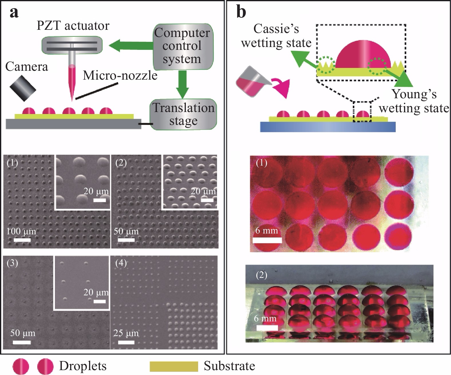
Fig. 3 MLAs created via microdroplet manipulation.
a Schematic diagram of microdroplet jetting system and MLA with different sizes via microdroplet jetting45. Reprinted with permission. Copyright 2020, OSA. b Schematic diagram of wettability-controlled microdroplets and microdroplets lens array based on wettability control46. Reprinted with permission. Copyright 2015, RSC. -
Wettability is an important property of solid surfaces; it depends on the microstructure and chemical composition of a material. The contact angle of liquid droplets and solid materials can be manipulated by programming the chemical composition or microstructures of the surface. In certain cases, a droplet deposited on a substrate forms a spherical surface under the surface tension effect, functioning as a microlens. Inspired by this phenomenon, microdroplet lens arrays based on structured substrates have garnered considerable attention (Fig. 3b)46-48. For example, a liquid MLA based on oil droplets created using an underwater superoleophobic pattern has been proposed. The shape of the oil lens is adjustable by the pattern and the oil volume (Fig. 3b)46. Recently, some tunable liquid lens arrays based on electrowetting have emerged, in which the curvature of the liquid lenses can be controlled by the electrostatic force of an external electric field49, 50. The fabrication of MLAs via wettability manipulation has been investigated comprehensively for simple processes and economic materials; however, 100% fill factor and curved MLAs are not realisable using this method.
-
UPM based on a fast tool servo (FTS) is an essential technique that enables a freeform optical surface. In this process, an ultrahard material such as diamond serves as a tooltip to remove the target material point by point using a computer control system, as shown in Fig. 4a-b51-55. FTS-assisted UPM is suitable for various materials, including typical metals (aluminium alloys and copper alloys), polymers, and brittle materials. Based on different driving principles, UPM can be classified into ultraprecision grinding, ultraprecision milling, slow slide servo/slow tool servo turning, and fly cutting. Among them, the former three are widely used for creating MLAs with precise shapes56-63. For example, Roeder et al. proposed a polymer MLA created via ultraprecision milling and successfully applied the MLA in a hyperspectral imaging system (Fig. 4c-d)57. In addition to traditional planar MLAs, UPM has been widely investigated for fabricating 3D MLAs with freeform surfaces. Li et al. fabricated a freeform MLA with a large FOV of 48° × 48° and a thickness of 1.6 mm (Fig. 4e)59. The proposed MLA comprises 8 × 8 microlenses, each of which is individually designed for a specific spatial direction. Dunkel et al. demonstrated a double-sided refractive freeform array, with each side containing 15 × 9 single microlenses, in which every single lenslet was optimised to the best shape to minimise optical aberrations, and the adjacent lenses were closely bounded (100% fill factor) by vertical edges60. The final ACE yielded a resolution of 720P, demonstrating its significant potential for commercial imaging devices (Fig. 4f). Although UPM is a real 3D processing method, it still presents some disadvantages. For instance, the diamond cutting tool wears continuously with usage; this not only affects the surface roughness of MLAs, but also increases the cost compared with other methods.
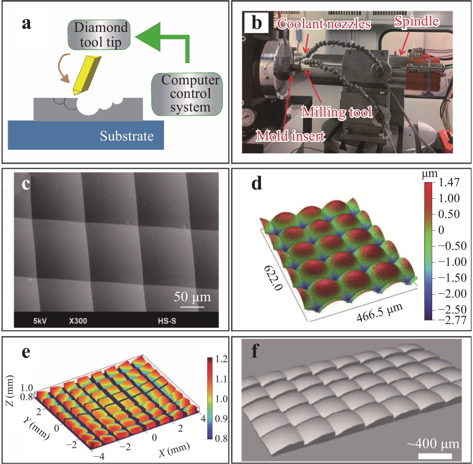
Fig. 4 MLAs created via ultraprecision machining.
a Schematic diagram of ultraprecision machining. b Photograph of ultraprecision machining setup57. Copyright 2018, MDPI. Surface profile of planar MLA c, d57 and free-form MLA e, f59, 60 via ultraprecision machining. Reprinted from ref. 57 with permission. Reprinted from refs. 59, 60 with permission. Copyright 2012, OSA. -
Fs-laser manufacturing has been recognised as one of the most promising techniques for fabricating microstructures such as ACEs with designable 3D structures, high precision, and compact size. The fs-laser offers advantages of ultrashort pulse widths of approximately hundreds of femtoseconds and an extremely high energy density up to 1013 W/μm2 64-67. The high energy of fs-lasers render them compatible with various types of materials, from soft to hard materials19, 68-71. An extreme spatial resolution of tens of nanometres, which is beyond the limits of optical diffraction, can be realised owing to the nonlinear absorption effect68, 72-73. In addition, fs-laser processing is performed by scanning the focus point layer by layer based on a predesigned pattern. Therefore, programmable 3D microstructures as complicated as curved CE lenses can be yielded easily.
Fs-laser manufacturing includes two types of processing: a subtractive manufacturing process based on fs-laser ablation (FsLA) and an additive manufacturing process based on two-photon or multiphoton induced polymerisation. A detailed review is provided in the following section.
-
Subtractive fs-laser manufacturing is based on the laser ablation process, in which a pulsed fs-laser is focused onto a substrate to remove (ablate) small fractions of the substrate material or chemically modify the ablated region64, 65. The high energy of the fs-laser pulse endows it the ability to process hard materials, such as silicon, sapphire, and diamond74-85. FsLA has been considered and used for technical applications in micro-optics and microelectronics for years.
The FsLA process comprises two steps, i.e. an ablation process and an etching process (Fig. 5a). First, the fs-laser scans on the substrate point by point and form an array of microholes, since some of the substrate is removed. The chemical properties (chemical energy and chemical composition) of the remaining irradiated area are modified because of the high-energy laser pulse. In addition, the surface roughness increases compared with that of the untreated area. Subsequently, an etching process is performed for two reasons. First, because the etching rate of the modified region is much faster than that of the untreated region owing to the different chemical properties, an MLA with the desired curved surface will be formed. Second, the etching process smoothes the rough surface of the irradiated region—a necessary process for high-quality optics. Specifically, two types of etching-assisted FsLA processes exist: wet-etching-assisted fs-laser ablation (WE-FsLA)74-80 and dry-etching-assisted fs-laser ablation (DE-FsLA)81-85.
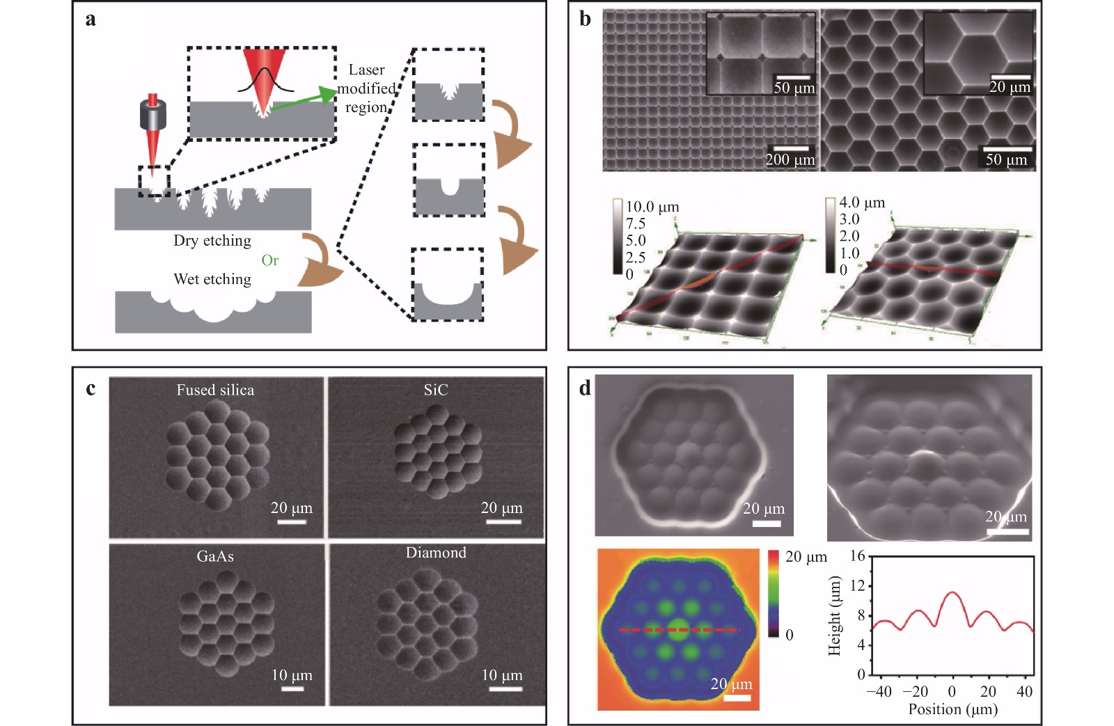
Fig. 5 MLAs created via subtractive laser manufacturing.
The wet etching process uses chemical reagents with strong corrosiveness, such as hydrofluoric acid. It has been widely used to smooth rough surfaces after FsLA owing to its high efficiency. For example, Chen et al. performed WE-FsLA to fabricate a close-packed MLA on a silica glass with rectangular and hexagonal concave surfaces, where the diameters of the rectangular and hexagonal microlenses were 67.05 and 30.54 μm, respectively (Fig. 5b)86. In addition to silica glass, the WE-FsLA process is suitable for other hard materials such as Polydimethylsiloxane (PDMS)87, BK7 glass88, and PMMA89.
Despite the high efficiency and adaptability of many materials, chemical wet-etching can result in distorted structures caused by lateral etching, which is detrimental to device integration. Although many materials can be processed via chemical wet-etching, the latter is still a material-dependent process. Therefore, DE-FsLA has been proposed to address this issue. In general, etching processes that do not involve any chemical liquid can be regarded as dry-etching, including ion beam etching (IBE), inductively coupled plasma (ICP), reactive ion etching (RIE), and focused ion beam etching. During the dry-etching process, plasmas or etchant gases remove the fs-laser-irradiated substrate material using high kinetic energy or chemical reactions. Specifically, the IBE process is a physical reaction process using high-energy plasma to dispel atoms from the substrate. For ICP and RIE processes, in addition to physical reactions, chemical reactions (vapour-phase etching) occur in which chemical vapour etches the substrate. DE-FsLA is a highly accurate technology that can be flexibly controlled by changing the laser power, pulse number, and etching time. In addition, because dry-etching can be applied on almost any hard material, MLAs based on various substrates have been proposed81-85. Fig. 5c shows concave hexagonal microlenses on fused silica, GaAs, SiC, and diamond85.
In addition to WE-FsLA and DE-FsLA, high-temperature annealing has been proposed to smooth the surface after FsLA. A convex MLA with independent focal lengths is shown in Fig. 5d. It has been reported that the surface roughness of the microstructure can be reduced from 100 to 3 nm through high-temperature annealing at 1250°C for 1 h90.
Because FsLA is a subtractive process, fs-laser ablated structures often serve as a moulding template, and the convex structure is typically obtained via a subsequent thermal casting process. Liu et al. proposed a centimetre-sized 3D CE with more than 190 000 close-packed ommatidia (20 µm in diameter and 1.5 µm in height) using concave moulding (Fig. 6b)[78]. The fabrication process is shown in Fig. 6a; the concave MLA was produced via the DE-FsLA of a glass substrate, and the final convex MLA was made of K9 glass. Similarly, Hao et al. fabricated a convex CE lens (5 mm in diameter) with 3000 close-packed microlenses (95 µm in diameter). In this case, the moulding was obtained by the WE-FsLA of a curved sapphire substrate, and the final CE lens was fabricated using PDMS[83].
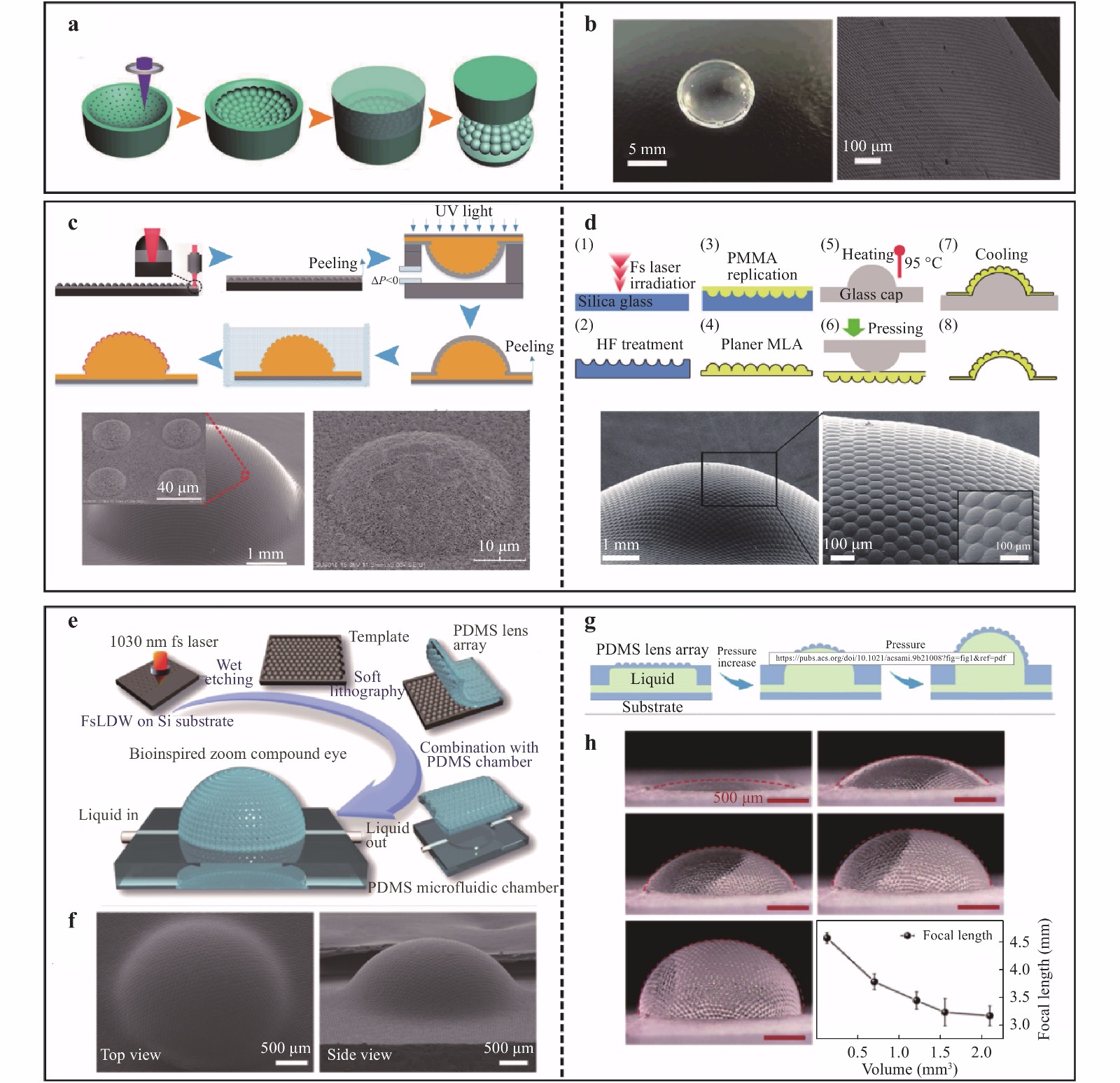
Fig. 6 Subtractive laser manufacturing of 3D MLAs.
a–b Direct fabrication of 3D MLA on concave substrate via DE-FsLDW78. Reprinted with permission. Copyright 2019, Wiley. c–d 3D MLA by shape deformation of planar MLA91, 92. Reprinted with permission. Copyright 2019, ACS. Reprinted with permission. Copyright 2012, AIP. e–h Tunable 3D MLA via WE-FsLDW94. Reprinted with permission. Copyright 2020, ACS.Another method to achieve curved/3D ACEs is by changing the shape of plane MLAs mechanically79, 91-93. Typically, thermal casting is performed first. A convex planar MLA is replicated using a fs-laser-ablated concave MLA as a moulding template. Subsequently, an external force (mechanical press or air pressure) is applied on the convex MLA, deforming the MLA to a curved ACE. The 3D ACEs created via air- and glass-bead-assisted deformations are presented in Fig. 6c91-d,92 respectively.
In addition to MLAs with defined shapes, tunable ACEs with advanced focusing ability have been proposed94, 95. Cao et al. successfully fabricated a zoom ACE via WE-FsLA, enabling variable focus imaging (Fig. 6e)94. Both the focal length (3.03 mm to infinity) and FOV (0-180°) can be adjusted by changing the volume of water in the microcavity (Fig. 6g-h).
-
Additive laser manufacturing is based on the two-photon absorption (TPA) or multiphoton absorption of photosensitive polymer materials, such as photoresists96, proteins97, liquid crystals98, and soft polymers70. The photons are absorbed nonlinearly at the extreme high-power density point, of which the volume is much smaller than the cubic wavelength72. Therefore, high-resolution TPA fs-laser manufacturing up to tens of nanometres, i.e. beyond the optical diffraction limit, can be achieved. Additive fs-laser manufacturing has garnered significant research interest in micro-optics, micromachines, microelectronics, and microfluidic chips96-103.
Fig. 7a shows a schematic diagram of the TPA fs-laser process. First, the photosensitive polymer material was deposited onto the glass substrate. Subsequently, under the point-by-point irradiation of the fs-laser, the radiated area was polymerised through TPA. Owing to the difference in solubility of certain solvents, the unexposed parts will be removed by the subsequent rinsing process, resulting in only the predesigned structures.
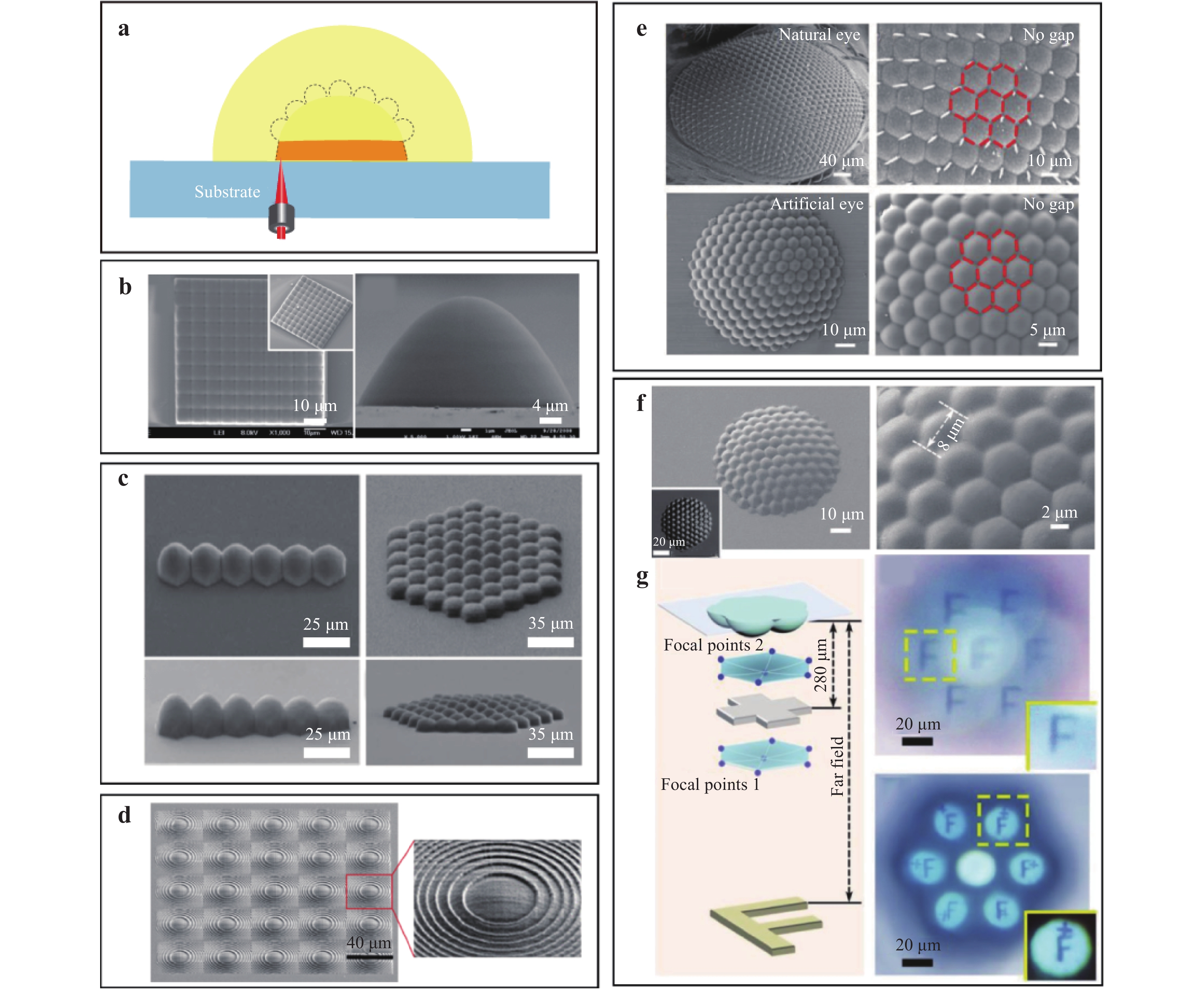
Fig. 7 Additive laser manufacturing of MLAs.
a Schematic diagram of additive laser manufacturing via TPA/MPA. b MLA with designed aspheric surface99. Reprinted with permission. Copyright 2009, IEEE. c MLA with individual focus lengths100. Reprinted with permission. Copyright 2015 OSA. d Fresnel MLA101. Copyright 2020, MDPI e 3D MLA via additive LDW19. Reprinted with permission. Copyright 2014, Wiley. f, g Tunable BSA MLA via additive LDW102. Reprinted with permission. Copyright 2019, Wiley.As a 3D direct writing process, TPA fs-laser manufacturing can yield freeform MLAs, such as MLAs with aspheric microlenses or nonuniform MLAs with individual surface profiles. Hence, optical aberrations induced by an uncontrollable surface can be optimised. For example, to reduce spherical aberration, Wu et al. introduced a close-packed and well-defined MLA with aspheric surfaces. The average error of such a microlens was less than 0.2% (the smallest value reported in 2009) (Fig. 7b)99. Tian et al. demonstrated a planar ACE with individual curvature unit lenses based on the SU-8 resist, providing a solution to the problem of field curvature aberration (Fig. 7c)100. Yan et al. proposed a Fresnel MLA based on the SZ2080 resist with modified focusing and imaging performance (Fig. 7d)101. Furthermore, 3D ACEs with curved surfaces have been achieved via TPA fs-laser manufacturing. Wu et al. reported a high-quality 3D ACE with small dimensions (total diameter ~84 μm), a high fill factor (100%), and an ultralow surface roughness (2.5 nm) (Fig. 7e)19.
Based on the tunable response of polymer materials applied in TPA fs-laser manufacturing, ACEs with focusing capability have been achieved. For example, the bovine serum albumin (BSA) protein is highly sensitive to the pH condition of the surrounding environment, demonstrating swelling and shrinking under different pH conditions. Based on this phenomenon, Ma et al. fabricated a BSA CE with variable focal imaging (Fig. 7f)102, where the FOV is adjustable from 35° at pH 5 to 80° at pH 13, and the focal length can be tuned up to 400%. Fig. 7g shows the dynamic tuning process for such an ACE. By changing the pH values (10 and 4), clear images of the ‘+’ pattern and the letter ‘F’ are obtained.
Fs-laser processing is regarded as the most promising nanofabrication technology owing to its high fabrication accuracy, designability of arbitrary-shape structures, and 3D processing capacity. However, concerns regarding its low processing efficiency arising from the point-by-point scanning model have emerged. Hence, several strategies have been developed, including shell prototyping, voxel-modulation, and spatial light modulation104-109.
Shell prototyping and voxel-modulation methods have been developed for TPA fs-laser manufacturing. In shell prototyping, only the surface layer of the desired structure is irradiated by the fs-laser, whereas the inner material is solidified by additional UV exposure104-105. It has been reported that the fabrication time of a chain structure can be reduced significantly from 20 h to 30 min104. As shown in Fig. 8a, various structures with fine and smooth surfaces were fabricated through the prototyping of nanoshells, such as a standalone hemisphere with holes, large-volume cuboids, and 100% fill-factor hexagonal MLAs104. Another similar solution for improving the speed of fs-laser fabrication is voxel modulation. As a point-by-point scanning process, the distance of each fs-laser point (voxel distance) is tunable. Precise scanning with a small voxel distance is time consuming compared with large voxel distance scanning. Meanwhile, large-voxel-distance scanning can result in a high surface roughness. Therefore, by balancing these two factors, the combination of small and large voxel scanning can afford the fast fabrication of high-quality structures (Fig. 8b)19. A 3D ACE has been proposed as a proof-of-concept; it only required 0.85 h (3.04 × 10⁶ voxels), whereas precise scanning (4.86 × 10⁷ voxels) required 13.6 h at the maximum (Fig. 8c)19.
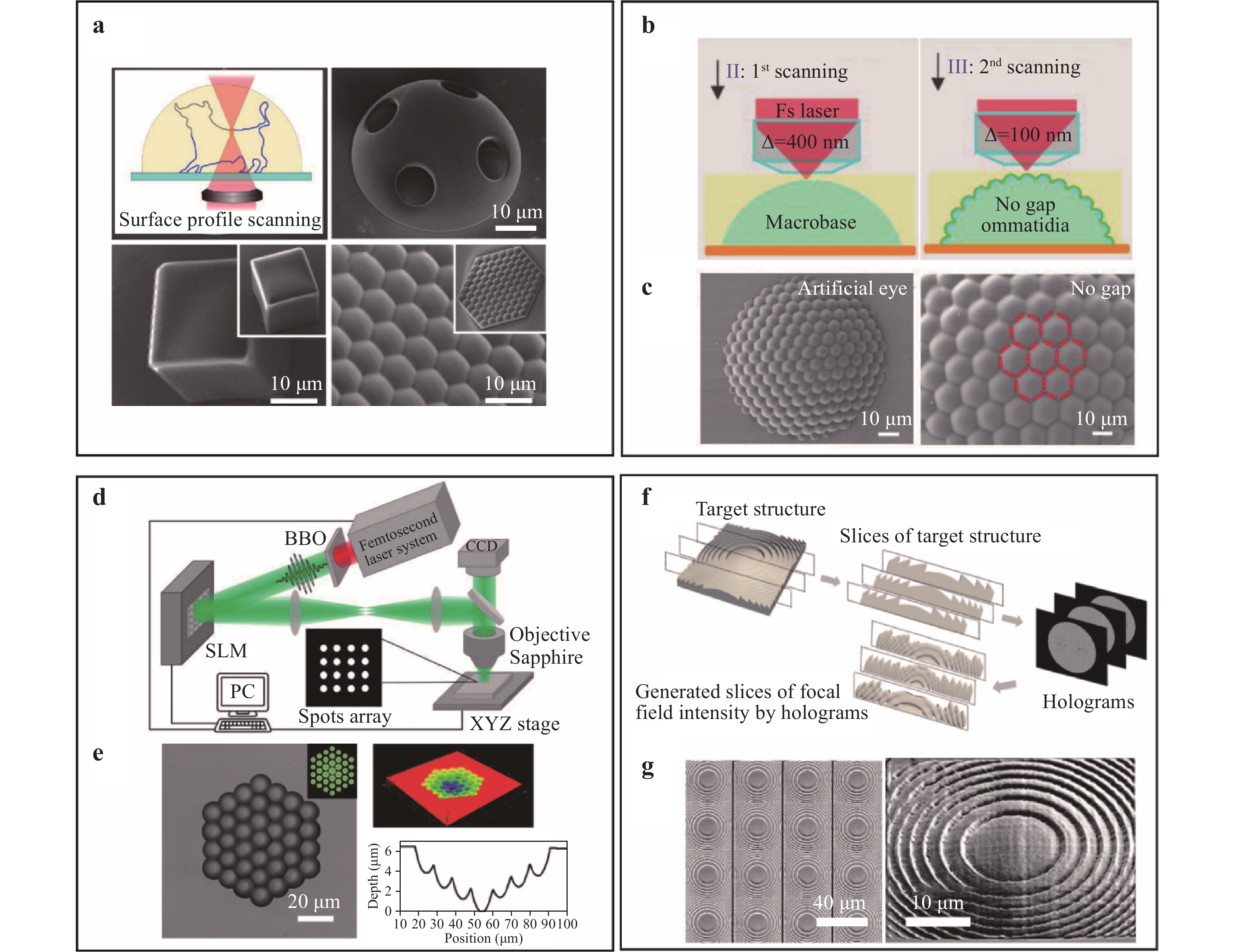
Fig. 8 Strategies for improving fabrication efficiency of femtosecond laser processing.
a Shell prototyping of microstructures68,105. Reprinted with permission. Copyright 2009, Elsevier68. Reprinted with permission. Copyright 2009, RSC105. b, c 3D MLA via voxel-modulation FsLDW19. Reprinted with permission. Copyright 2014, Wiley. Spatial light modulation of fs-laser for subtractive laser manufacturing d, e107,108 and additive laser manufacturing f, g101.107,108 Reprinted with permission. Copyright 2020, OSA.101 Copyright 2020, MDPI.In addition to the former two methods, spatial light modulation can be used to fabricate large-sized structures rapidly; this method is applicable to both subtractive106-108 and additive fs-laser manufacturing101, 109. Spatial light modulators (SLMs) are used to modulate the light information in space and time, including amplitude, phase, or polarisation. In the case of subtractive fs-laser manufacturing, one spot laser beam is segmented into multiple spots using an SLM. A microhole array can be easily obtained using only one single laser pulse; hence, the fabrication process can be accelerated significantly. Based on this theory, Cao et al. designed and fabricated a 3D CE lens array using a phase-only SLM, and the ACE demonstrated excellent imaging performance in various focus planes (Fig. 8d)107. For spatial light modulation in additive laser manufacturing, the focal points of the fs-laser are engineered into ultrathin focal planes, followed by a one-dimensional scanning of the corresponding slices individually; finally, a 3D structure is obtained. A Fresnel MLA has been created via focal field engineering, in which only 7 s was required for fabricating one microlens (Fig. 8f)101.
Fs-laser manufacturing is one of the most ideal approaches for fabricating ACEs with miniature size, high accuracy, and programmable morphology. We believe that with further improvements in large-scale production, fs-laser manufacturing will become one of the main methods for fabricating miniature ACEs.
-
With the significant advantages of large FOV, large depth of field, and high sensitivity to dynamic objects, ACEs offer great potential for advanced applications, including microrobot vision, unmanned aerial vehicle detection, and medical diagnosis. In the following section, several examples of large FOV imaging, depth estimation, and 3D imaging are provided to illustrate the broad application of ACE.
(ⅰ) Large FOV imaging One of the most desirable features of natural CEs is their extremely large observation range; furthermore, some of them can achieve a maximum FOV of 360°. Consequently, applications in large FOV imaging have been widely investigated16, 17, 110-111. In terms of large FOV imaging, ACEs with a curved surface have a larger FOV compared with planar ACEs.
For example, Floreano et al. proposed the CurvACE camera, which comprises three functionally different layers, a polymer lens array with a low reflective aperture system, and a photodetector array that is integrated into a flexible PCB16. By cutting the plane ACEs with high-precision grinding and mechanical bending, a curved ACE with an FOV of 180° × 60° was obtained. The angular sensitivity function along the horizontal and vertical directions was measured, as shown in Fig. 9a, and most of them exhibited the expected Gaussian distribution, thereby validating the desirable micro-optical design and precise alignment.
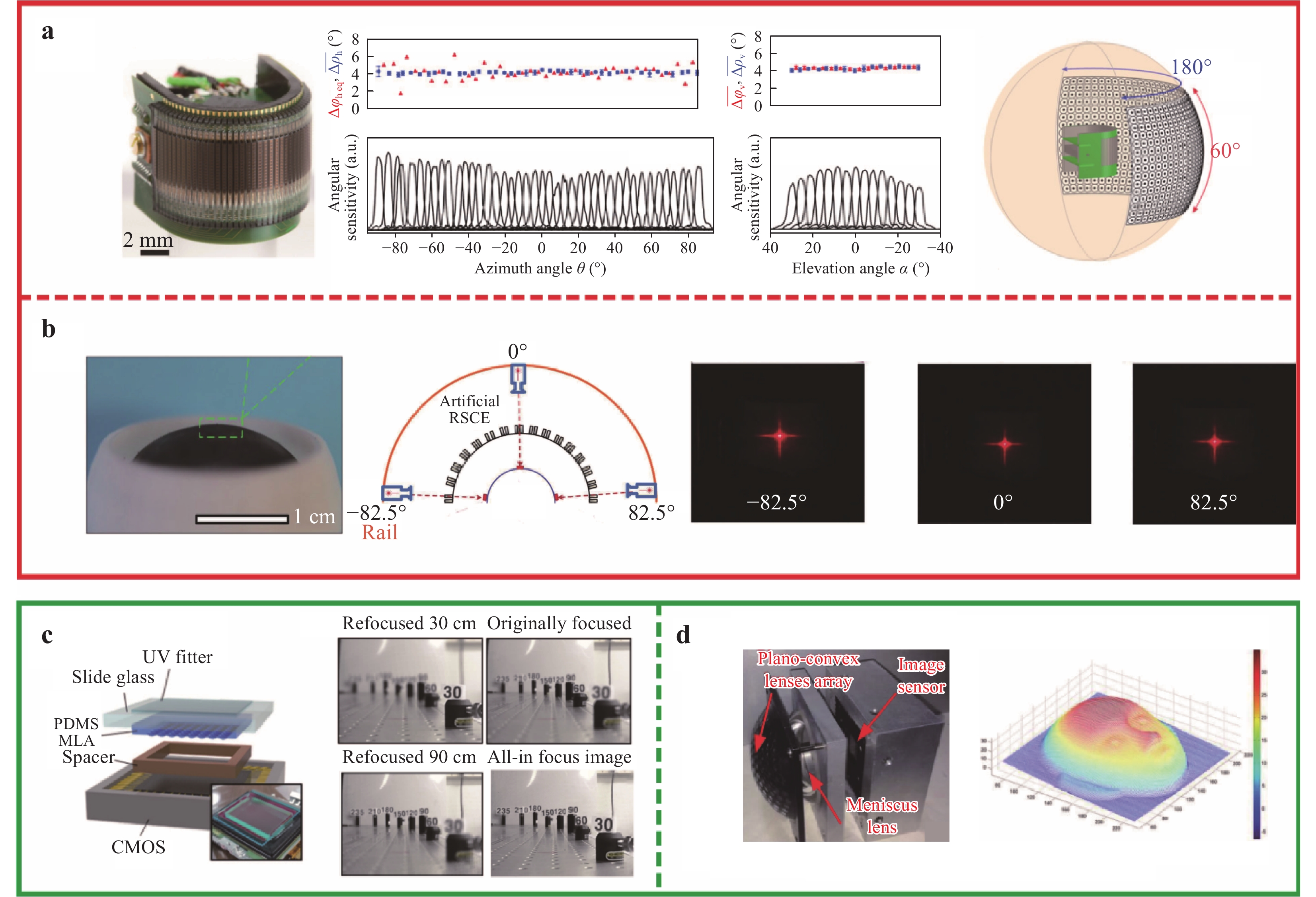
Fig. 9 Applications of ACEs.
Large FOV imaging of CurvACE a16 and RSCEs b111. c Depth estimation of light field camera35 d 3D reconstruction of ACE system113.16 Copyright 2013, National Academy of Sciences.111 Reprinted with permission. Copyright 2020, Wiley.35 Reprinted with permission. Copyright 2019, OSA.111 Reprinted with permission. Copyright 2014, OSA.In the same year, Song et al. developed a digital camera inspired by natural arthropod eyes17. First, an array of 16 × 16 microlenses was assembled into a square elastomer substrate (PDMS). Meanwhile, a stretchable photodetector array comprising photodiodes and blocking diodes was fabricated in a grid pattern. Subsequently, a 3D ACE was fabricated by combining the two soft layers and elastically transforming them into a hemispherical geometry with a spherical supporting substrate made of solid PDMS. The arthropod-inspired camera possessed a total FOV of 160°, i.e. almost a full hemisphere. Furthermore, multiple objects at different angles and distances can be captured simultaneously.
In addition to refraction devices, Huang et al. proposed a reflection superposition compound eye (RSCE) that can achieve large FOV imaging110. A 410 × 410 array of high-aspect-ratio Si square-microtubes was fabricated on a Silicon-On-Insulator (SOI) wafer and then transferred to a transparent and flexible hemispherical PDMS membrane with a curvature of 1.1 cm. The RSCEs camera had an exceptional FOV of up to 165° and high imaging quality without distortion because the reflection-based device was not affected by chromatic aberrations from optical material dispersion. The imaging performance of the large FOV is shown in Fig. 9b. It is noteworthy that the detector responded promptly as the light source travelled from −82.5° to 82.5°, thereby demonstrating the real-time motion detection capability of the RSCEs.
(ⅱ) 3D reconstruction and depth estimation Humans can easily determine whether an object is far or near to them because the human eye is a typical binocular vision system that is sensitive to 3D information. Images from two eyes exhibit minor disparities but share an overlapping view. By processing two images from the same scene with these slight differences, our brain can acquire a single stereo image. Similarly, ACEs (whether planar ACEs or curved ACEs) with multi-overlapping views are applicable to depth estimation and 3D reconstruction, referred to as the multiview stereo vision system35, 112-113.
Kin et al. fabricated a light field system with four-dimensional information based on MLAs with diverse focus lengths via etching-assisted photolithography35. An all-in-focusing image can be reconstructed from a single exposure. The imaging processing results are shown in Fig. 9c; refocused images at 30 and 90 cm were reconstructed from the original focusing image at 60 cm, and an all-in-focused image was obtained using the focal stacking method.
Similarly, Lee et al. proposed a depth-estimation-enabled computational compound eye (COMPU-EYE) imaging system was proposed112. An iterative reconstruction algorithm (sparse-representation-based classification) was proposed for improving the image quality with depth information. The performance of the depth estimation for objects was investigated, and the letters from each distance were observed and reconstructed with a 1.56 times improvement from 80 × 80 to 100 × 100 pixels.
Ma et al. designed an ACE system comprising a 3D MLA and a beam-steering lens for object detection in 3D spaces113. The detected points can be located accurately using the proposed calibration method. Subsequently, a human face sculpture was scanned and reconstructed with approximately 10,000 scanning points, demonstrating potential for 3D object detection (Fig. 9d).
ACE cameras, which afford depth estimation and 3D reconstruction, can be applied to not only stereo imaging, but also to future applications in 3D flow measurement, 3D motion detection, etc.113-116
-
ACE devices have emerged as highly promising imaging systems owing to their large FOV, extended field depth, and outstanding sensitivity for moving objects. Compared with large camera arrays, miniaturised ACEs with light weight, small size, and compact structure have been continuously pursued to satisfy the increasing requirements in the fields of microrobot vision, in-vivo medical imaging devices, etc. Significant effort has been expended toward the fabrication of ACEs, resulting in significant progress in imaging industries and advanced fields such as biomedicine and robots.
Regarding the fabrication of ACEs, various techniques have been proposed, from photolithography to fs-laser manufacturing. A qualified fabrication method should satisfy the high-precision manufacture of closed packed and curved MLAs. In addition, the accuracy control of the surface morphology of each microlens is crucial for high-quality imaging. Based on these requirements, we evaluated the fabrication methods, as follows: Photolithography and strategies based on microdroplets could not control the surface morphology of the microlenses, and most of them could not yield MLAs with 100% fill factor; hence, high-quality focusing and full utilisation of incoming lights could not be achieved. In addition, photolithography and droplet manipulation methods are planar techniques; planar MLAs require complicated processes, including shape-changing, to implement a hemispheric shape. Nevertheless, as a commercial processing technology, photolithography has matured and high accuracy production can be achieved easily. Meanwhile, diamond ultraprecision milling and fs-laser manufacturing are real 3D manufacturing processes that guarantee the close-packed arrangement of microlenses on a curved surface. We predict that they will be used widely for the fabrication of 3D MLAs in the coming years. In particular, fs-laser manufacturing is highly recommended for its extremely high resolution beyond the optical diffraction limits (tens of nanometres).
With rapid developments in the fabrication of curved MLAs, ACEs, particularly 3D ACEs, have been widely investigated for their significant potential in wide-angle imaging, depth estimation, and 3D imaging. However, challenges such as the fabrication of curved image sensors and resolution improvement must be addressed in future research.
(ⅰ) Fabrication of curved image sensors
As mentioned previously, 3D ACEs are necessitated for large FOV imaging. To obtain an image, MLAs must be assembled with the image sensors. However, most existing image receptor arrays (CCD, CMOS) are planar compositions, and it is clear that curved MLAs are incompatible with commercial planar image sensors. To match curved MLAs with planar image sensors, nonhomogeneous focus MLAs and light relay systems have been proposed39, 116-118. Nevertheless, 3D ACEs with planar image sensors are affected by significant challenges in terms of correction algorithms aimed at off-axis aberrations. In addition, the optical relay device is complicated to fabricate and unfavourable for compact devices. Therefore, the fabrication of curved image sensors, which are regarded as an ideal match to curved MLAs, is a significant issue.
Recently, with the development of flexible printed circuit boards (FPCBs), ACEs based on curved image sensors have been developed, such as the CurvACE camera proposed by Floreano et al.16 and the digital camera proposed by Song et al.17. Curved photodetection arrays based on silicon nanorods119 and two-dimensional materials120 have been reported. Gu et al. presented a novel hemispherical photoreceptor comprising a high-density array of nanowires121, which demonstrated the potential for high-quality imaging and 3D optical sensing.
Although technological advances in flexible electronics have promoted the development of 3D ACEs that provide large FOV observations, the FPCB industry is still in the early stage of development and the high-accuracy fabrication of compact sensor arrays should be further investigated. Owing to rapid developments in of science and technology, strategies to achieve high-quality manufacturing of flexible image sensors are anticipated. It is noteworthy that fs-laser manufacturing has been proven to be compatible with the IC fabrication process82. The combination of high-quality 3D MLAs fabricated using fs-laser and miniature flexible image sensors may enable the development of next-generation ACE devices.
(ⅱ) Strategies for high-resolution imaging CEs possess an inferior resolution compared with the human eyes owing to their inherent structural constraints, such as the small aperture of ommatidium, which do not facilitate artificial imaging devices. However, it has been reported that the imaging quality of previously reported ACEs is much lower than that of traditional cameras. One of the strategies for resolution improvement is to optimise the relevant algorithm. For example, based on a previous digital camera17, Lee et al. proposed a COMPU-EYE system with improved resolution based on modified modern digital signal processing in 2016122. Another possible solution is to optimise the microlenses or design new types of microlenses with advanced imaging abilities, such as metalenses123-127. Metalenses are flat, ultrathin metasurfaces that can manipulate light waves by introducing phase delay via subwave nanostructures (nanoantennas). Compared with traditional lenses, metalenses offer numerous advantages such as achromaticism (no chromatic aberrations) and polarisation sensitivity. Additionally, the production of metalenses is compatible with the standard CMOS digital technique, which permits wafer-scale integration. ACEs based on metalenses may emerge as a new type of advanced optics for high-quality imaging.
In conclusion, with upcoming technologies, miniature ACE cameras with larger FOVs, better imaging performances, and more compact structures will be realised. These devices may become indispensable to our future daily lives.
-
The authors acknowledge the National Natural Science Foundation of China under Grants and National Key Research and Development Program of China #61935008, #61775078, #61905087, #61590930, and #2017YFB1104600 for support.
Miniaturising artificial compound eyes based on advanced micronanofabrication techniques
-
Lin Zhu1,
 ,
, -
Yong-Lai Zhang1, *, ,
,
-
Hong-Bo Sun2, *, ,
- Light: Advanced Manufacturing 2, Article number: (2021)
- Received: 29 July 2020
- Revised: 19 January 2021
- Accepted: 28 January 2021 Published online: 25 February 2021
doi: https://doi.org/10.37188/lam.2021.007
Abstract: Compound eyes (CEs) are advanced optical visual systems with distinct features of large view-fields, infinite depth of field, and dynamic imaging capability, revealing their significant potential in applications including robot vision, unmanned aerial vehicle detection, and medical diagnosis. Compared with macroscopic CEs, which primarily comprise multicamera arrays, compact integrated CEs have garnered significant attention because of their portability and possibility of flexible integration with microrobots and in-vivo medical facilities. To date, considerable effort has been devoted to this field, in which manufacturing technologies are vital to the development of artificial CEs (ACEs) capable of large field-of-view imaging, depth information collection, and three-dimensional imaging. Challenges and opportunities exist for the practical application of advanced ACEs. This paper reviews state-of-the-art technologies for manufacturing ACEs, and then briefly summarises their potential applications in different fields. Finally, the current challenges and perspectives of ACEs are discussed.
Research Summary
Artificial compound eyes: inspiration for advanced camera systems.
Compound eyes of arthropods are advanced and fascinating visual systems with distinct features of small sizes, large view-fields, infinite depths of field, and dynamic imaging capability. Thus far, considerable efforts have been devoted to the fabrication of artificial compound eye cameras due to their promising applications in robotic vision, unmanned aerial vehicle detection, and medical diagnosis. Hong-Bo Sun from Tsinghua University and his colleagues reviewed state-of-the-art technologies for manufacturing artificial compound eye cameras and also discussed challenges and perspectives for their future applications.
Rights and permissions
Open Access This article is licensed under a Creative Commons Attribution 4.0 International License, which permits use, sharing, adaptation, distribution and reproduction in any medium or format, as long as you give appropriate credit to the original author(s) and the source, provide a link to the Creative Commons license, and indicate if changes were made. The images or other third party material in this article are included in the article′s Creative Commons license, unless indicated otherwise in a credit line to the material. If material is not included in the article′s Creative Commons license and your intended use is not permitted by statutory regulation or exceeds the permitted use, you will need to obtain permission directly from the copyright holder. To view a copy of this license, visit http://creativecommons.org/licenses/by/4.0/.

 DownLoad: